| ID |
Date |
Author |
Subject |
|
606
|
Wed Apr 19 12:17:25 2017 |
Stefan Ritt | Wave rotation during transfer from the board? | This is correct. Actually the amplitude array is rotated already inside the DRS4 chip. So the readout starts with the stop cell plus one. If you do not do anything, the waveform is already "rotated". If you want the waveform to start with physical cell #0, you have to "unrotate" it.
Stefan
| Strahinja Lukic wrote: |
|
Is this correct, and does this mean that the amplitude array is "rotated" already during the transfer from the board?
|
|
|
607
|
Thu Apr 20 06:30:13 2017 |
Strahinja Lukic | Wave rotation during transfer from the board? | Thanks.
Strahinja
| Stefan Ritt wrote: |
|
This is correct. Actually the amplitude array is rotated already inside the DRS4 chip. So the readout starts with the stop cell plus one. If you do not do anything, the waveform is already "rotated". If you want the waveform to start with physical cell #0, you have to "unrotate" it.
Stefan
| Strahinja Lukic wrote: |
|
Is this correct, and does this mean that the amplitude array is "rotated" already during the transfer from the board?
|
|
|
|
657
|
Tue Feb 27 13:17:00 2018 |
Steven Block | WIndows Connection problem with drs507 SOLVED | Hello All,
I too have been struggling with trying to get the drs4 (507) to work on my windows machine and I found it to be a problem with the libusb library. My solution is as follows and has worked on multiple PC's. I ran this solution after I first plugged in the drs4 and installed 507.
Go to http://zadig.akeo.ie/ and install the corresponding software.
After that, you will need to plug in the DRS4 to your computer. From there go to ‘Options’, and select ‘List all Devices’.
Finally, choose the DRS4 evaluation board from the list and press install driver and let it run. You should be fine after that.
Best,
Steven |
|
658
|
Tue Feb 27 13:29:47 2018 |
Stefan Ritt | WIndows Connection problem with drs507 SOLVED | Dear Steven, many thanks for this information, this is very useful. I know of people having problems on Windows 10, maybe this will also help them.
Stefan
| Steven Block wrote: |
|
Hello All,
I too have been struggling with trying to get the drs4 (507) to work on my windows machine and I found it to be a problem with the libusb library. My solution is as follows and has worked on multiple PC's. I ran this solution after I first plugged in the drs4 and installed 507.
Go to http://zadig.akeo.ie/ and install the corresponding software.
After that, you will need to plug in the DRS4 to your computer. From there go to ‘Options’, and select ‘List all Devices’.
Finally, choose the DRS4 evaluation board from the list and press install driver and let it run. You should be fine after that.
Best,
Steven
|
|
|
695
|
Wed May 9 14:07:10 2018 |
Alec Shackleford | WIndows Connection problem with drs507 SOLVED | Thank you for this fantastic solution. I had almost reinstalled windows 7 to see if that would solve the issue!
All the best,
Alec
| Stefan Ritt wrote: |
|
Dear Steven, many thanks for this information, this is very useful. I know of people having problems on Windows 10, maybe this will also help them.
Stefan
| Steven Block wrote: |
|
Hello All,
I too have been struggling with trying to get the drs4 (507) to work on my windows machine and I found it to be a problem with the libusb library. My solution is as follows and has worked on multiple PC's. I ran this solution after I first plugged in the drs4 and installed 507.
Go to http://zadig.akeo.ie/ and install the corresponding software.
After that, you will need to plug in the DRS4 to your computer. From there go to ‘Options’, and select ‘List all Devices’.
Finally, choose the DRS4 evaluation board from the list and press install driver and let it run. You should be fine after that.
Best,
Steven
|
|
|
|
696
|
Mon May 14 09:21:29 2018 |
Alessio Berti | WIndows Connection problem with drs507 SOLVED | Hi,
I have a machine with Windows 10 and the solution provided by Steven works fine. To give more details, the driver installed in my case is WinUSB (i.e. libusb, v6.1.7600.16385).
Cheers,
Alessio
| Alec Shackleford wrote: |
|
Thank you for this fantastic solution. I had almost reinstalled windows 7 to see if that would solve the issue!
All the best,
Alec
| Stefan Ritt wrote: |
|
Dear Steven, many thanks for this information, this is very useful. I know of people having problems on Windows 10, maybe this will also help them.
Stefan
| Steven Block wrote: |
|
Hello All,
I too have been struggling with trying to get the drs4 (507) to work on my windows machine and I found it to be a problem with the libusb library. My solution is as follows and has worked on multiple PC's. I ran this solution after I first plugged in the drs4 and installed 507.
Go to http://zadig.akeo.ie/ and install the corresponding software.
After that, you will need to plug in the DRS4 to your computer. From there go to ‘Options’, and select ‘List all Devices’.
Finally, choose the DRS4 evaluation board from the list and press install driver and let it run. You should be fine after that.
Best,
Steven
|
|
|
|
|
678
|
Fri Apr 13 18:14:07 2018 |
Alessio Berti | Voltage and Timing Calibration in drs_exam.cpp | Hi,
we were trying to implement an automatic way to calibrate our DRS4 both in voltage and in time (we have the V5 Evaluation Board). We started from drs_exam.cpp and tried with the following lines:
/* set input range to -0.5V ... +0.5V */
b->SetInputRange(0);
b->CalibrateVolt(NULL);
b->CalibrateTiming(NULL);
While the timing calibration seems to work (we checked with drsosc executable), the voltage calibration in our test program seems not to do the same as in drsosc when pressing the button "Execute Voltage Calibration". Specifically we think that no primary calibration, secondary calibration or spike removal is applied when calling CalibrateVolt(). It seems that the methods to perform those tasks are implemented in Osci.ccp/Osci.h, but drs_exam.cpp uses objects of the class DRS (i.e. defined in DRS.cpp and DRS.h).
Is there a way to execute the voltage calibration in drs_exam.cpp in the same way performed within drsosc?
Cheers,
Alessio |
|
687
|
Fri May 4 11:56:08 2018 |
Stefan Ritt | Voltage and Timing Calibration in drs_exam.cpp | Have you set the sampling frequency
b->SetFrequency(5, true);
before the calibration?
Note there is also the "drscl" program, which is a ocmmand linke interface to the evaluation board. Start it, and do the calibration there:
/drs4eb/software/drscl$ ./drscl
DRS command line tool, Revision 21435
Type 'help' for a list of available commands.
Found DRS4 board 0 on USB, serial #2400, firmware revision 30000
B0> freq 5
B0> calib
Enter calibration frequency [GHz]: 5
Enter range [V]: 0
Enter mode [1]024 or [2]048 bin mode: 1
Please make sure that no input signal are present then hit any key
Creating Calibration of Board on USB, serial #2400
B0> ===============================================]
B0>
then look at the code in drscl.cpp (around line 1097).
/Stefan
| Alessio Berti wrote: |
|
Hi,
we were trying to implement an automatic way to calibrate our DRS4 both in voltage and in time (we have the V5 Evaluation Board). We started from drs_exam.cpp and tried with the following lines:
/* set input range to -0.5V ... +0.5V */
b->SetInputRange(0);
b->CalibrateVolt(NULL);
b->CalibrateTiming(NULL);
While the timing calibration seems to work (we checked with drsosc executable), the voltage calibration in our test program seems not to do the same as in drsosc when pressing the button "Execute Voltage Calibration". Specifically we think that no primary calibration, secondary calibration or spike removal is applied when calling CalibrateVolt(). It seems that the methods to perform those tasks are implemented in Osci.ccp/Osci.h, but drs_exam.cpp uses objects of the class DRS (i.e. defined in DRS.cpp and DRS.h).
Is there a way to execute the voltage calibration in drs_exam.cpp in the same way performed within drsosc?
Cheers,
Alessio
|
|
|
Draft
|
Wed Oct 7 13:06:34 2015 |
Ilja Bekman | Voltage Calibration with signal on the input | |
|
13
|
Wed Oct 7 17:58:20 2009 |
Stefan Ritt | VDD switch off speed | It turned out that the VDD switch off speed plays some important role. On our VME board, we have a linear regulator, then a 4.7 uF capacitor, then the DRS4 chip (DVDD and AVDD). When switching off the VME power, it takes quite some time to discharge the 4.7 uF capacitor, since the DRS4 chip goes into a high impedance mode if VDD < ~1V. This gives following VDD trace:
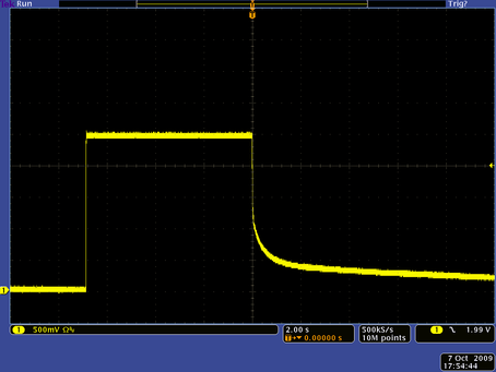
Rising edge is power on, falling edge is power off. Note the horizontal time scale of 2 s/div. So to get below 0.3 V or so, it takes up to 30 seconds. If the power is switched back on when AVDD is above 0.3V, the DRS4 chip can get into a weird state, where probably many domino waves are started and the chip draws an enormous amount of current. Typically the linear regulator limits the current, so the 2.5V drops to ~1.5V, and the board is not working. If people are aware of this and always wait >30sec. before turning the power on again, this is fine, but people might forget.
So the solution is to put a resistor (typically 100 Ohm to 1 kOhm) parallel to the 4.7 uF capacitor in order to have some resistive current load of a few mA. The discharge then looks like this:
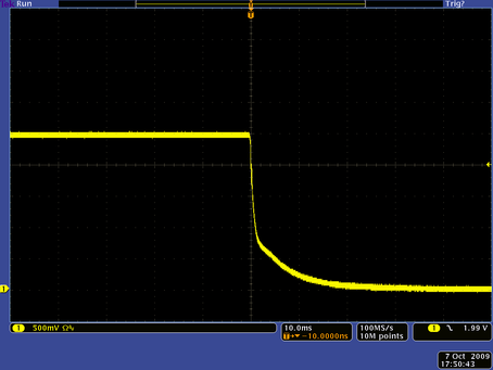
Note the horizontal scale of 10ms/div. So after 30 ms AVDD is discharged and powering on the chip again does not do any harm. The same should be done to DVDD. |
|
12
|
Tue Oct 6 11:20:39 2009 |
Stefan Ritt | VDD instability | It has turned out that the stability of the AVDD and DVDD power supplies for the DRS4 are very critical. On the evaluation board I use a REG1117-2.5, on our VME board I use a ADP3338-2.5 for the DVDD power supply. When the domino wave is started, the power consumption of the DRS4 chip jumps up by ~40 mA, which has to be compensated by the linear regulator. Following screen shot shows what happens:
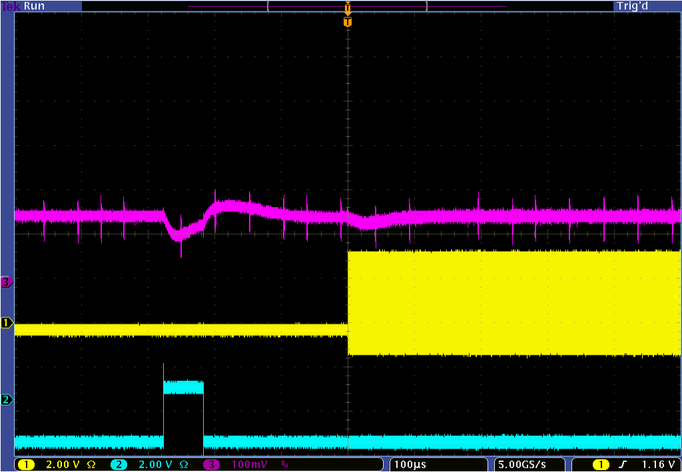
The blue trace is the DWRITE signal indicating the sampling phase when high. The yellow is the SRCLK showing when the readout takes place. The pink is now the DVDD power. It can be clearly seen that there is a dip of ~50 mV when the domino wave starts, a positive dip when it stops and another smaller dip when the readout starts. This causes strange effects: If the trigger arrives during the first dip, the actual sampling takes place when the DVDD is ~50 mV smaller, which leads to a baseline shift of a sampled 0V DC input voltage of about the same amount (-50 mV).
The obvious improvement is to put a huge capacitor on the power supply, but that does not help much:
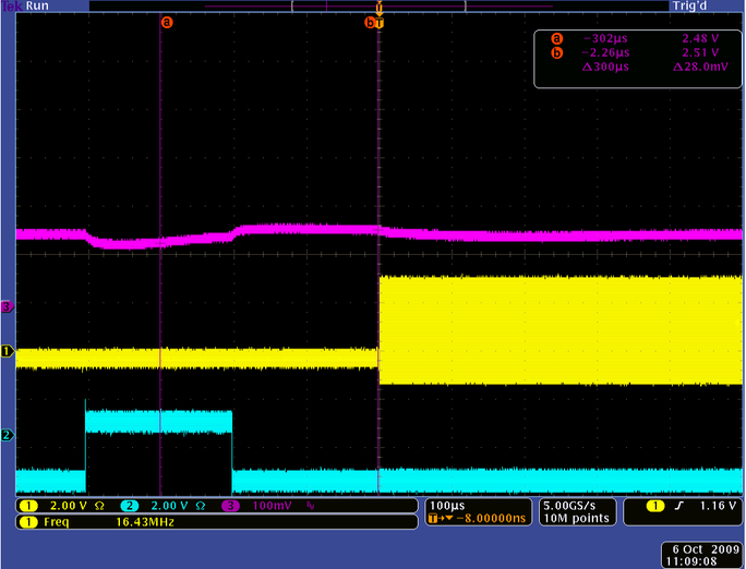
The dip gets a bit smaller, but it's still there. So a better solution would be to use a faster LDO regulator. Please take care of this if you plan a new design.
Furthermore, I believe that the chip internally has some "warmup" phase, where the die heats up a bit when the additional 40 mA are drawn. So a "good" solution is to wait some time after starting the domino wave until one allows for triggers. Tests showed that a few milliseconds are necessary to keep the baseline shifts below a few millivolts. This of course decreases the dead time of the system significantly, so one has to choose the proper balance between increase dead time and increased base line shift. On some applications where a baseline shift is not an issue, one could opt for the minimum dead time. |
|
851
|
Tue Nov 16 01:27:51 2021 |
Jacquelynne Vaughan | V3 board, only one channel works, all components at each channel input working | Hi everyone,
I'm still looking through the forum for an answer to this question, but thought I'd go ahead and post anyway just in case it hasn't been answered yet. If it has I can take this post down.
I have a V3 board, and as far as I can tell only channel 2 gives an output. If I enable other channels using the DRS Oscilloscope software, they do show static but will not show a signal if I connect one to them (e.g. a series of subsequent square waves). A technician and I took the board out and tested all the components leading up to the microcontrollers for each channel, and everything seemed to be working fine. I thought maybe it was configured to only have one channel read an output, but I looked through the Config panel in the software and nothing seemed to indicate that.
I am a novice, and maybe I'm missing something that I didn't see in the manual. I can post screenshots if needed!
Thank you for your help! |
|
852
|
Tue Nov 16 08:51:14 2021 |
Stefan Ritt | V3 board, only one channel works, all components at each channel input working | A V3 boards is already 10 years old and out of warranty. The software has no configuration to turn channels off except the channel buttons on the main page on top of the sliders. I presume the channels are broked due to some overvoltage applied to them (the V5 board is better protected against over voltage). You can send it the board for repair, but it will cost almost the same amount of money than buying a new boards.
Regards,
Stefan
| Jacquelynne Vaughan wrote: |
|
Hi everyone,
I'm still looking through the forum for an answer to this question, but thought I'd go ahead and post anyway just in case it hasn't been answered yet. If it has I can take this post down.
I have a V3 board, and as far as I can tell only channel 2 gives an output. If I enable other channels using the DRS Oscilloscope software, they do show static but will not show a signal if I connect one to them (e.g. a series of subsequent square waves). A technician and I took the board out and tested all the components leading up to the microcontrollers for each channel, and everything seemed to be working fine. I thought maybe it was configured to only have one channel read an output, but I looked through the Config panel in the software and nothing seemed to indicate that.
I am a novice, and maybe I'm missing something that I didn't see in the manual. I can post screenshots if needed!
Thank you for your help!
|
|
|
467
|
Wed Jan 6 15:51:58 2016 |
Larry Byars | Use of Channel Cascading in drs_exam.cpp | Hello Stefan,
Here in Rockford, TN we just got a new DRS4 evaluation board (Serail # 2612, Board Type 9, Firmware 21305) which is labeled as combined 2048.
It looks like the drs_exam.cpp only works with 1024 samples per channel. We'd like to be able to get 2048 samples from each of the four channels but I am uncertain what code modifications are necessary support this.
Could you offer a suggestion? I've searched the forum for cascade and read several threads but they are pretty old. One even says it isn't supported in the evaluation board, but I think that is no longer the case.
Thanks for your help,
Larry Byars
|
|
469
|
Tue Jan 12 15:42:31 2016 |
Larry Byars | Use of Channel Cascading in drs_exam.cpp | An update. I have been successful in making modifications to drs_exam.cpp so that I can get 2048 samples per channel.. The main changes were to the size of the time_array and wave_array and adding a call to Set ChannelConfig(0,8,4). It was also necessary to change the parameters to GetWave so that the Trigger Cell and WSR values were passed to get the channel combinations correct (2048 channel.ppt).
I've moved on to try to increase the speed of acquisition (I get only about 500 events/sec) and trying to understand the corrections.Working through the source code slowly...
Regards,
Larry Byars
| Larry Byars wrote: |
|
Hello Stefan,
Here in Rockford, TN we just got a new DRS4 evaluation board (Serail # 2612, Board Type 9, Firmware 21305) which is labeled as combined 2048.
It looks like the drs_exam.cpp only works with 1024 samples per channel. We'd like to be able to get 2048 samples from each of the four channels but I am uncertain what code modifications are necessary support this.
Could you offer a suggestion? I've searched the forum for cascade and read several threads but they are pretty old. One even says it isn't supported in the evaluation board, but I think that is no longer the case.
Thanks for your help,
Larry Byars
|
|
|
470
|
Tue Jan 12 16:06:07 2016 |
Stefan Ritt | Use of Channel Cascading in drs_exam.cpp | Hi Larry,
sorry my late reply, swamped with work here. You were right in the modifictions you did, congrats. The speed limitation of 500 events come from USB2, which simply is not fast enough. The 500 Hz are mentioned on the evaluation board web site, so you should have seen that before ordering. Some people build their own hardware around the chip, in which case they get higher rates. The "hard" limit is the DRS4 readout speed, which is 30ns per sample. So if you have 8 ADCs in parallel, and you only need 100 samples of your waveform, the readout time is 3 us, in which case you could go up to a few 10 kHz without much of a dead time.
Cheers,
Stefan
| Larry Byars wrote: |
|
An update. I have been successful in making modifications to drs_exam.cpp so that I can get 2048 samples per channel.. The main changes were to the size of the time_array and wave_array and adding a call to Set ChannelConfig(0,8,4). It was also necessary to change the parameters to GetWave so that the Trigger Cell and WSR values were passed to get the channel combinations correct (2048 channel.ppt).
I've moved on to try to increase the speed of acquisition (I get only about 500 events/sec) and trying to understand the corrections.Working through the source code slowly...
Regards,
Larry Byars
| Larry Byars wrote: |
|
Hello Stefan,
Here in Rockford, TN we just got a new DRS4 evaluation board (Serail # 2612, Board Type 9, Firmware 21305) which is labeled as combined 2048.
It looks like the drs_exam.cpp only works with 1024 samples per channel. We'd like to be able to get 2048 samples from each of the four channels but I am uncertain what code modifications are necessary support this.
Could you offer a suggestion? I've searched the forum for cascade and read several threads but they are pretty old. One even says it isn't supported in the evaluation board, but I think that is no longer the case.
Thanks for your help,
Larry Byars
|
|
|
|
820
|
Wed Apr 7 03:29:39 2021 |
Sean Quinn | Unexpected noise in muxout: t_samp related? | Dear DRS4 team,
I'm experiencing some issues that seem to be isolated to the ASIC, and would like to understand if we are doing something wrong. There are several items to address in the post.
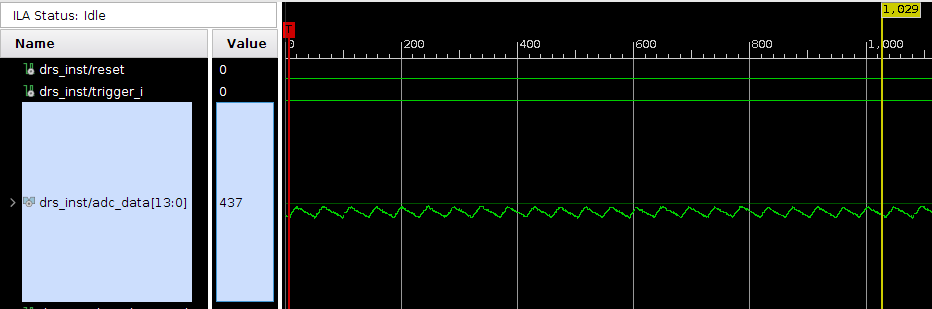
First, I do not think the noise observed is being injected from elsewhere on the board. If I run the DRS in transparent mode, the baseline noise is low, on order 3.5 mV (60 ADU), perhaps radiated from a clock. See below image. The scale is 0 to 1000 ADU with LSB = 6 uV (same AD9245 as eval board.). The DRS is in RUNNING state, I have forced a trigger in the ILA. This is for a single channel, CH0, 1024 cells.
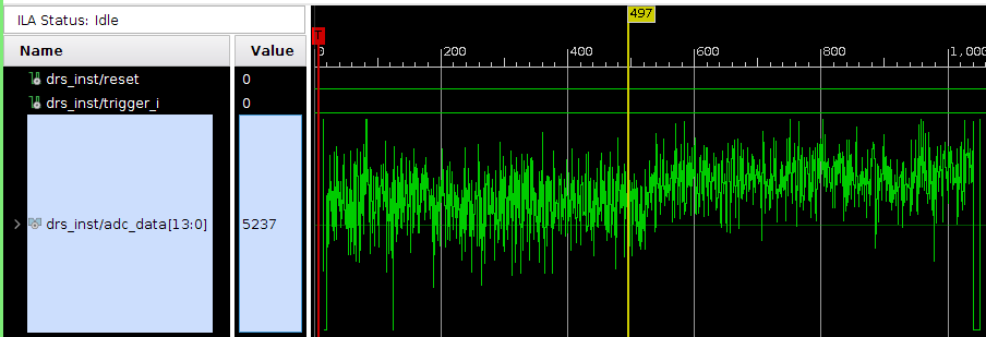
In the next image, I show the waveform obtained from a full readout. This corresponds to ADC_READOUT state, and the plot uses the same 1000 ADU scale. Noise seems around 350 ADU now, many factors worse than before.
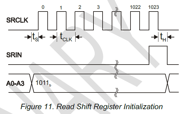
We've spent a lot of time trying to understand what's happening. One area that would be helpful to get some guidance on is the "t_samp" parameter. In Fig. 11 of the data sheet, should there be a t_samp label between t_s and t_clk? It just has arrows there with some width.
In our current firmware I believe R1 is simply one clock after R0 (for both ROI and full readout mode). Would this lead to the added noise observed in muxout?
This leads to the next question on what to actually use for t_samp. In the data sheet, page 4 "Timing Characteristics" it says to use t_samp = t0 + t_clk. Additionally, t0= 10 ns from that table. Fair enough.
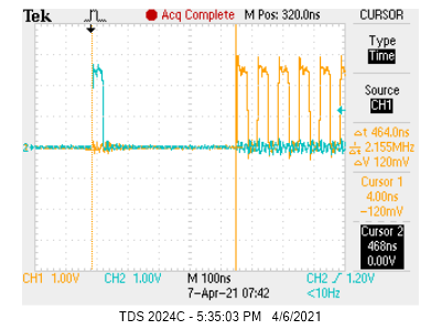
But if I check this against the eval board timing, I see very different values. Here the clock is 15 MHz so t_clk=67 ns (I note another post about this topic https://elog.psi.ch/elogs/DRS4+Forum/713), so I expect t_samp = 77 ns. But in practice it looks like the R0 to R1 delay is ~465 ns? (cyan=RSRLOAD, yellow=SRCLK)
Given this, is t_samp a value that should be tuned by the user?
Best regards,
Sean
|
|
821
|
Wed Apr 7 08:26:12 2021 |
Stefan Ritt | Unexpected noise in muxout: t_samp related? | Dear Sean,
noise in transparent mode comes from some coupling to your system clock. But 3.5 mV RMS seems rather hight to me. You should get it to below 1 mV if the DRS4 input is clean (try to short it).
The noise in the readout is expected. It looks exactly as Plot3 from the data sheet. You have to calibrate it away with a fixed offset for each cell as described in this paper: https://arxiv.org/abs/1405.4975 (paragraph IV. A. Voltage Calibration).
Concerning t_samp: Fig 11 in the datasheet just tells you that the rising edge of the SRCLK should come later than t_s after the address change. t_s is the setup time and 5 ns. Fig 12 tells you that the ADC should sample the analog output of the DRS t_samp after the address change A0-A3 and t_samp after the rising edge of SRCLK.
The digitizing speed of the evaluation board is indeed 15 MHz instead of the maximum 30 MHz, because this was easier to program in the FPGA. The t_samp has to be there so that the analog output signal of the DRS4 settles to its final value after each SRCLK pulse. If you sample "too early", you sample with the ADC the output when it is sill moving. So you have to wait until the analog is settled, but just before the next DRS sample becomes visible at the output. You can fine tune this with a differential probe at the DRS4 analog output (on a single ended probe you might drown in noise) on one channel of yoru scope and the ADC sample clock on the other channel of your scope. Note that the ADC sample clock cannot be derived straight from your FPGA clock, but you need some clock manager to fine-adjust its phase in 1ns steps.
But again, looking at your output, everything seems fine. You see the 5mV rms noise indicated in the datasheet table 1, which translates to about 20 mV peak-to-peak. If you do the offset calibration, this should go down to below 1 mV.
Best,
Stefan
| Sean Quinn wrote: |
|
Dear DRS4 team,
I'm experiencing some issues that seem to be isolated to the ASIC, and would like to understand if we are doing something wrong. There are several items to address in the post.
First, I do not think the noise observed is being injected from elsewhere on the board. If I run the DRS in transparent mode, the baseline noise is low, on order 3.5 mV (60 ADU), perhaps radiated from a clock. See below image. The scale is 0 to 1000 ADU with LSB = 6 uV (same AD9245 as eval board.). The DRS is in RUNNING state, I have forced a trigger in the ILA. This is for a single channel, CH0, 1024 cells.
In the next image, I show the waveform obtained from a full readout. This corresponds to ADC_READOUT state, and the plot uses the same 1000 ADU scale. Noise seems around 350 ADU now, many factors worse than before.
We've spent a lot of time trying to understand what's happening. One area that would be helpful to get some guidance on is the "t_samp" parameter. In Fig. 11 of the data sheet, should there be a t_samp label between t_s and t_clk? It just has arrows there with some width.
In our current firmware I believe R1 is simply one clock after R0 (for both ROI and full readout mode). Would this lead to the added noise observed in muxout?
This leads to the next question on what to actually use for t_samp. In the data sheet, page 4 "Timing Characteristics" it says to use t_samp = t0 + t_clk. Additionally, t0= 10 ns from that table. Fair enough.
But if I check this against the eval board timing, I see very different values. Here the clock is 15 MHz so t_clk=67 ns (I note another post about this topic https://elog.psi.ch/elogs/DRS4+Forum/713), so I expect t_samp = 77 ns. But in practice it looks like the R0 to R1 delay is ~465 ns? (cyan=RSRLOAD, yellow=SRCLK)
Given this, is t_samp a value that should be tuned by the user?
Best regards,
Sean
|
|
|
822
|
Fri Apr 9 20:22:13 2021 |
Sean Quinn | Unexpected noise in muxout: t_samp related? | Hi Stefan,
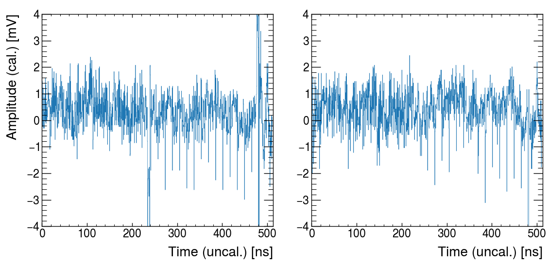
Thanks much for the quick reply. Ok, yes, things do seem ok after the offset calibration. I am running into some other issues I could use your advice on but will make a separate thread. As a preview, you can see hints in this waveform (periodic negative spikes).
This one should be considered resolved.
| Stefan Ritt wrote: |
|
Dear Sean,
noise in transparent mode comes from some coupling to your system clock. But 3.5 mV RMS seems rather hight to me. You should get it to below 1 mV if the DRS4 input is clean (try to short it).
The noise in the readout is expected. It looks exactly as Plot3 from the data sheet. You have to calibrate it away with a fixed offset for each cell as described in this paper: https://arxiv.org/abs/1405.4975 (paragraph IV. A. Voltage Calibration).
Concerning t_samp: Fig 11 in the datasheet just tells you that the rising edge of the SRCLK should come later than t_s after the address change. t_s is the setup time and 5 ns. Fig 12 tells you that the ADC should sample the analog output of the DRS t_samp after the address change A0-A3 and t_samp after the rising edge of SRCLK.
The digitizing speed of the evaluation board is indeed 15 MHz instead of the maximum 30 MHz, because this was easier to program in the FPGA. The t_samp has to be there so that the analog output signal of the DRS4 settles to its final value after each SRCLK pulse. If you sample "too early", you sample with the ADC the output when it is sill moving. So you have to wait until the analog is settled, but just before the next DRS sample becomes visible at the output. You can fine tune this with a differential probe at the DRS4 analog output (on a single ended probe you might drown in noise) on one channel of yoru scope and the ADC sample clock on the other channel of your scope. Note that the ADC sample clock cannot be derived straight from your FPGA clock, but you need some clock manager to fine-adjust its phase in 1ns steps.
But again, looking at your output, everything seems fine. You see the 5mV rms noise indicated in the datasheet table 1, which translates to about 20 mV peak-to-peak. If you do the offset calibration, this should go down to below 1 mV.
Best,
Stefan
| Sean Quinn wrote: |
|
Dear DRS4 team,
I'm experiencing some issues that seem to be isolated to the ASIC, and would like to understand if we are doing something wrong. There are several items to address in the post.
First, I do not think the noise observed is being injected from elsewhere on the board. If I run the DRS in transparent mode, the baseline noise is low, on order 3.5 mV (60 ADU), perhaps radiated from a clock. See below image. The scale is 0 to 1000 ADU with LSB = 6 uV (same AD9245 as eval board.). The DRS is in RUNNING state, I have forced a trigger in the ILA. This is for a single channel, CH0, 1024 cells.
In the next image, I show the waveform obtained from a full readout. This corresponds to ADC_READOUT state, and the plot uses the same 1000 ADU scale. Noise seems around 350 ADU now, many factors worse than before.
We've spent a lot of time trying to understand what's happening. One area that would be helpful to get some guidance on is the "t_samp" parameter. In Fig. 11 of the data sheet, should there be a t_samp label between t_s and t_clk? It just has arrows there with some width.
In our current firmware I believe R1 is simply one clock after R0 (for both ROI and full readout mode). Would this lead to the added noise observed in muxout?
This leads to the next question on what to actually use for t_samp. In the data sheet, page 4 "Timing Characteristics" it says to use t_samp = t0 + t_clk. Additionally, t0= 10 ns from that table. Fair enough.
But if I check this against the eval board timing, I see very different values. Here the clock is 15 MHz so t_clk=67 ns (I note another post about this topic https://elog.psi.ch/elogs/DRS4+Forum/713), so I expect t_samp = 77 ns. But in practice it looks like the R0 to R1 delay is ~465 ns? (cyan=RSRLOAD, yellow=SRCLK)
Given this, is t_samp a value that should be tuned by the user?
Best regards,
Sean
|
|
|
|
824
|
Fri Apr 9 20:55:28 2021 |
Stefan Ritt | Unexpected noise in muxout: t_samp related? | If you do the cell calibration correctly, your noise should be ~0.4 mV. You seem to be 2-3x larger. The periodic negative spikes come if you dont' sample at the right time. Adjust t_samp until they are gone.
Stefan
| Sean Quinn wrote: |
|
Hi Stefan,
Thanks much for the quick reply. Ok, yes, things do seem ok after the offset calibration. I am running into some other issues I could use your advice on but will make a separate thread. As a preview, you can see hints in this waveform (periodic negative spikes).
This one should be considered resolved.
| Stefan Ritt wrote: |
|
Dear Sean,
noise in transparent mode comes from some coupling to your system clock. But 3.5 mV RMS seems rather hight to me. You should get it to below 1 mV if the DRS4 input is clean (try to short it).
The noise in the readout is expected. It looks exactly as Plot3 from the data sheet. You have to calibrate it away with a fixed offset for each cell as described in this paper: https://arxiv.org/abs/1405.4975 (paragraph IV. A. Voltage Calibration).
Concerning t_samp: Fig 11 in the datasheet just tells you that the rising edge of the SRCLK should come later than t_s after the address change. t_s is the setup time and 5 ns. Fig 12 tells you that the ADC should sample the analog output of the DRS t_samp after the address change A0-A3 and t_samp after the rising edge of SRCLK.
The digitizing speed of the evaluation board is indeed 15 MHz instead of the maximum 30 MHz, because this was easier to program in the FPGA. The t_samp has to be there so that the analog output signal of the DRS4 settles to its final value after each SRCLK pulse. If you sample "too early", you sample with the ADC the output when it is sill moving. So you have to wait until the analog is settled, but just before the next DRS sample becomes visible at the output. You can fine tune this with a differential probe at the DRS4 analog output (on a single ended probe you might drown in noise) on one channel of yoru scope and the ADC sample clock on the other channel of your scope. Note that the ADC sample clock cannot be derived straight from your FPGA clock, but you need some clock manager to fine-adjust its phase in 1ns steps.
But again, looking at your output, everything seems fine. You see the 5mV rms noise indicated in the datasheet table 1, which translates to about 20 mV peak-to-peak. If you do the offset calibration, this should go down to below 1 mV.
Best,
Stefan
| Sean Quinn wrote: |
|
Dear DRS4 team,
I'm experiencing some issues that seem to be isolated to the ASIC, and would like to understand if we are doing something wrong. There are several items to address in the post.
First, I do not think the noise observed is being injected from elsewhere on the board. If I run the DRS in transparent mode, the baseline noise is low, on order 3.5 mV (60 ADU), perhaps radiated from a clock. See below image. The scale is 0 to 1000 ADU with LSB = 6 uV (same AD9245 as eval board.). The DRS is in RUNNING state, I have forced a trigger in the ILA. This is for a single channel, CH0, 1024 cells.
In the next image, I show the waveform obtained from a full readout. This corresponds to ADC_READOUT state, and the plot uses the same 1000 ADU scale. Noise seems around 350 ADU now, many factors worse than before.
We've spent a lot of time trying to understand what's happening. One area that would be helpful to get some guidance on is the "t_samp" parameter. In Fig. 11 of the data sheet, should there be a t_samp label between t_s and t_clk? It just has arrows there with some width.
In our current firmware I believe R1 is simply one clock after R0 (for both ROI and full readout mode). Would this lead to the added noise observed in muxout?
This leads to the next question on what to actually use for t_samp. In the data sheet, page 4 "Timing Characteristics" it says to use t_samp = t0 + t_clk. Additionally, t0= 10 ns from that table. Fair enough.
But if I check this against the eval board timing, I see very different values. Here the clock is 15 MHz so t_clk=67 ns (I note another post about this topic https://elog.psi.ch/elogs/DRS4+Forum/713), so I expect t_samp = 77 ns. But in practice it looks like the R0 to R1 delay is ~465 ns? (cyan=RSRLOAD, yellow=SRCLK)
Given this, is t_samp a value that should be tuned by the user?
Best regards,
Sean
|
|
|
|
|