ID |
Date |
Author |
Subject |
|
21
|
Fri Oct 30 03:31:54 2009 |
Jinhong Wang | outline dimension of DRS4 | 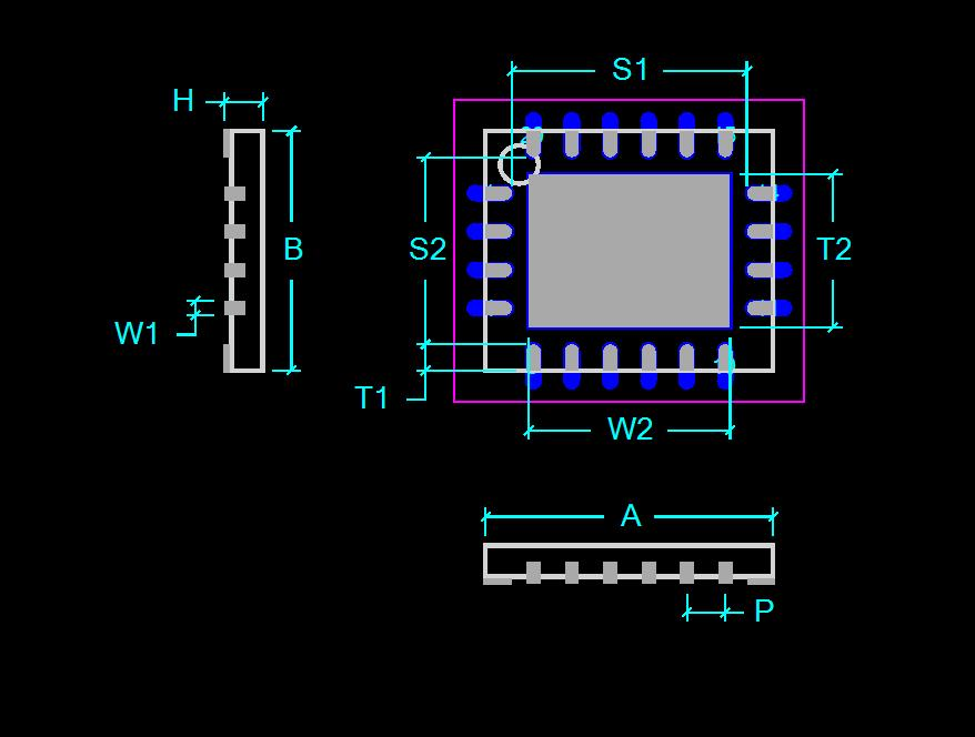
Fig.1 typical dimension of QFN package
Above is the typical dimension specification for QFN package. I cann't find the corresponding "T1" as in Fig.1 in the DRS4 documents, nor any of the tolerance of the dimensions, which are usually expressed in the form of a range between a min. value and a max. value.
So will you specify the dimension of "T1" and "W1", and the dimension tolerance of them?
Thanks and best wishes!
Jinhong Wang University of Science and Technology of China |
|
22
|
Wed Nov 4 14:42:22 2009 |
Stefan Ritt | outline dimension of DRS4 |
| Jinhong Wang wrote: |
|
Fig.1 typical dimension of QFN package
Above is the typical dimension specification for QFN package. I cann't find the corresponding "T1" as in Fig.1 in the DRS4 documents, nor any of the tolerance of the dimensions, which are usually expressed in the form of a range between a min. value and a max. value.
So will you specify the dimension of "T1" and "W1", and the dimension tolerance of them?
Thanks and best wishes!
Jinhong Wang University of Science and Technology of China
|
Please find attached the complete dimensions. |
| Attachment 1: qfn76.png
|

|
|
23
|
Mon Dec 14 10:14:16 2009 |
Jinhong Wang | Trigger of DRS4 | Dear Mr. S. Ritt
The following is my confusion about the trigger of DRS4. It mainly concertrates on the generation of trigger signal to stop DRS4 sampling process for readout of sampled waveform.
As metioned in the datasheet of DRS4, the chip samples the analog input every domino sampling period. After finished sampling a waveform, the sampling process can be stoped by lowering the DWRITE while keeping DENABLE high. But the analog input is asychronous to the Domino CLK. Then, how can we know when to stop the domino sampling process to read out the sampled waveform? Of course, a trigger can be used. But from my present knowledge of DRS4, trigger can only be generated from analog input. Analog input is splited into two channels, one to DRS4 analog input, the other to FPGA as the trigger. However, splitting analog inputs increases the system design complexity, and may lower the total performace. So what is your suggestion?
In our system, there are 8 analog inputs to a signal DRS4 chip, the outputs of DRS4 chip are connected to an 8-channel 14 bit ADC ( AD9252). It wold be kind of you to inform me about the most applicable approach for readout of DRS4 sampled wavefrom.
Best regards.
Sincerely,
Jinhong Wang (wangjinh@mail.ustc.edu.cn) |
|
24
|
Tue Dec 15 14:38:09 2009 |
Stefan Ritt | Trigger of DRS4 |
| Jinhong Wang wrote: |
|
Dear Mr. S. Ritt
The following is my confusion about the trigger of DRS4. It mainly concertrates on the generation of trigger signal to stop DRS4 sampling process for readout of sampled waveform.
As metioned in the datasheet of DRS4, the chip samples the analog input every domino sampling period. After finished sampling a waveform, the sampling process can be stoped by lowering the DWRITE while keeping DENABLE high. But the analog input is asychronous to the Domino CLK. Then, how can we know when to stop the domino sampling process to read out the sampled waveform? Of course, a trigger can be used. But from my present knowledge of DRS4, trigger can only be generated from analog input. Analog input is splited into two channels, one to DRS4 analog input, the other to FPGA as the trigger. However, splitting analog inputs increases the system design complexity, and may lower the total performace. So what is your suggestion?
In our system, there are 8 analog inputs to a signal DRS4 chip, the outputs of DRS4 chip are connected to an 8-channel 14 bit ADC ( AD9252). It wold be kind of you to inform me about the most applicable approach for readout of DRS4 sampled wavefrom.
Best regards.
Sincerely,
Jinhong Wang (wangjinh@mail.ustc.edu.cn)
|
Indeed you have to make an external trigger. The evaluation board uses the "transparent mode" of the DRS4 to "mirror" the input signal at the output, then puts a comparator there. The schematics of the evaluation board is in the manual. This does then not degrate the analog performance. You can of course also split the signal at the input, this will only add a minor additional load to the input signal, since the load of the DRS4 chips itself is much bigger than that of any comparator.
An alternative is to turn on the transparent mode and continuously digitize all 8 outputs with your AD9252. Then you make the trigger purely digital in your FPGA. You can put there a comparator, or even more complex logic like multiplicity etc. Note however that this causes some latency, since the ADC has a pipeline which is quite long, so you have to buffer the latency of your trigger in the analog window of the DRS4 sampling cells. Like if you run the DRS4 at 1 GSPS, you can accomodate 1024 ns of sampling depth, which is good for maybe 500 ns of trigger latency plus 500 ns of the waveform of interest. |
|
25
|
Mon Dec 21 10:17:05 2009 |
Jinhong Wang | Trigger of DRS4 |
| Stefan Ritt wrote: |
|
| Jinhong Wang wrote: |
|
Dear Mr. S. Ritt
The following is my confusion about the trigger of DRS4. It mainly concertrates on the generation of trigger signal to stop DRS4 sampling process for readout of sampled waveform.
As metioned in the datasheet of DRS4, the chip samples the analog input every domino sampling period. After finished sampling a waveform, the sampling process can be stoped by lowering the DWRITE while keeping DENABLE high. But the analog input is asychronous to the Domino CLK. Then, how can we know when to stop the domino sampling process to read out the sampled waveform? Of course, a trigger can be used. But from my present knowledge of DRS4, trigger can only be generated from analog input. Analog input is splited into two channels, one to DRS4 analog input, the other to FPGA as the trigger. However, splitting analog inputs increases the system design complexity, and may lower the total performace. So what is your suggestion?
In our system, there are 8 analog inputs to a signal DRS4 chip, the outputs of DRS4 chip are connected to an 8-channel 14 bit ADC ( AD9252). It wold be kind of you to inform me about the most applicable approach for readout of DRS4 sampled wavefrom.
Best regards.
Sincerely,
Jinhong Wang (wangjinh@mail.ustc.edu.cn)
|
Indeed you have to make an external trigger. The evaluation board uses the "transparent mode" of the DRS4 to "mirror" the input signal at the output, then puts a comparator there. The schematics of the evaluation board is in the manual. This does then not degrate the analog performance. You can of course also split the signal at the input, this will only add a minor additional load to the input signal, since the load of the DRS4 chips itself is much bigger than that of any comparator.
An alternative is to turn on the transparent mode and continuously digitize all 8 outputs with your AD9252. Then you make the trigger purely digital in your FPGA. You can put there a comparator, or even more complex logic like multiplicity etc. Note however that this causes some latency, since the ADC has a pipeline which is quite long, so you have to buffer the latency of your trigger in the analog window of the DRS4 sampling cells. Like if you run the DRS4 at 1 GSPS, you can accomodate 1024 ns of sampling depth, which is good for maybe 500 ns of trigger latency plus 500 ns of the waveform of interest.
|
Thank you. The transparent mode can be really helpful. Can you provide me in more details of the chip's transparent mode? I am still confused about the following aspects.
I notice that DRS4 samples the analog wave in the way "clear before write", and in the transparent mode, there will be certain delay before the trigger logic stops the sampling process. So,does it mean that the waveform recording process per Domino sampling cycle will not degrade the amplitude of the analog signal? Hence, for two idential analog inputs, one with a trigger latency of 500 ns and the other of 510 ns, the sampled waveform is identical, what differs is the starting number of the first active sampling cell, where the reading process considered to be started. Is that right? Looking forward to your insight.
Best regrads.
Sincerely,
Jinhong Wang (wangjinh@mail.ustc.edu.cn) |
|
26
|
Mon Dec 21 16:52:08 2009 |
Stefan Ritt | Trigger of DRS4 |
| Jinhong Wang wrote: |
|
| Stefan Ritt wrote: |
|
| Jinhong Wang wrote: |
|
Dear Mr. S. Ritt
The following is my confusion about the trigger of DRS4. It mainly concertrates on the generation of trigger signal to stop DRS4 sampling process for readout of sampled waveform.
As metioned in the datasheet of DRS4, the chip samples the analog input every domino sampling period. After finished sampling a waveform, the sampling process can be stoped by lowering the DWRITE while keeping DENABLE high. But the analog input is asychronous to the Domino CLK. Then, how can we know when to stop the domino sampling process to read out the sampled waveform? Of course, a trigger can be used. But from my present knowledge of DRS4, trigger can only be generated from analog input. Analog input is splited into two channels, one to DRS4 analog input, the other to FPGA as the trigger. However, splitting analog inputs increases the system design complexity, and may lower the total performace. So what is your suggestion?
In our system, there are 8 analog inputs to a signal DRS4 chip, the outputs of DRS4 chip are connected to an 8-channel 14 bit ADC ( AD9252). It wold be kind of you to inform me about the most applicable approach for readout of DRS4 sampled wavefrom.
Best regards.
Sincerely,
Jinhong Wang (wangjinh@mail.ustc.edu.cn)
|
Indeed you have to make an external trigger. The evaluation board uses the "transparent mode" of the DRS4 to "mirror" the input signal at the output, then puts a comparator there. The schematics of the evaluation board is in the manual. This does then not degrate the analog performance. You can of course also split the signal at the input, this will only add a minor additional load to the input signal, since the load of the DRS4 chips itself is much bigger than that of any comparator.
An alternative is to turn on the transparent mode and continuously digitize all 8 outputs with your AD9252. Then you make the trigger purely digital in your FPGA. You can put there a comparator, or even more complex logic like multiplicity etc. Note however that this causes some latency, since the ADC has a pipeline which is quite long, so you have to buffer the latency of your trigger in the analog window of the DRS4 sampling cells. Like if you run the DRS4 at 1 GSPS, you can accomodate 1024 ns of sampling depth, which is good for maybe 500 ns of trigger latency plus 500 ns of the waveform of interest.
|
Thank you. The transparent mode can be really helpful. Can you provide me in more details of the chip's transparent mode? I am still confused about the following aspects.
I notice that DRS4 samples the analog wave in the way "clear before write", and in the transparent mode, there will be certain delay before the trigger logic stops the sampling process. So,does it mean that the waveform recording process per Domino sampling cycle will not degrade the amplitude of the analog signal? Hence, for two idential analog inputs, one with a trigger latency of 500 ns and the other of 510 ns, the sampled waveform is identical, what differs is the starting number of the first active sampling cell, where the reading process considered to be started. Is that right? Looking forward to your insight.
Best regrads.
Sincerely,
Jinhong Wang (wangjinh@mail.ustc.edu.cn)
|
The amplitude of the analog signal is not degraded by the transparent mode, since the signal is buffered on the chip, and the output of this buffer is send off the chip. The waveform digitizing of course requires quite some current to charge up all capacitors, so there is maximum current of ~1mA for 5 GSPS. If you only have a weak signal source, your bandwidth might be limited by that. On the evaluation board for example we use passive transformers to produce the differential input signal from a single-ended signal. Although the transformers are rated 1 GHz Bandwidth, we only achieve 200 MHz with the passive transformers. By using active high speed differential drivers, you can get about 700 MHz right now.
If you have two channels with 500 ns and 510 ns trigger latency, there is no difference in the "domino stop position" since there is only one domino circuit per chip which can be stopped. So the stop position is the same for all eight channels on a chip. |
|
27
|
Tue Dec 22 01:30:55 2009 |
Jinhong Wang | Trigger of DRS4 |
| Stefan Ritt wrote: |
|
| Jinhong Wang wrote: |
|
| Stefan Ritt wrote: |
|
| Jinhong Wang wrote: |
|
Dear Mr. S. Ritt
The following is my confusion about the trigger of DRS4. It mainly concertrates on the generation of trigger signal to stop DRS4 sampling process for readout of sampled waveform.
As metioned in the datasheet of DRS4, the chip samples the analog input every domino sampling period. After finished sampling a waveform, the sampling process can be stoped by lowering the DWRITE while keeping DENABLE high. But the analog input is asychronous to the Domino CLK. Then, how can we know when to stop the domino sampling process to read out the sampled waveform? Of course, a trigger can be used. But from my present knowledge of DRS4, trigger can only be generated from analog input. Analog input is splited into two channels, one to DRS4 analog input, the other to FPGA as the trigger. However, splitting analog inputs increases the system design complexity, and may lower the total performace. So what is your suggestion?
In our system, there are 8 analog inputs to a signal DRS4 chip, the outputs of DRS4 chip are connected to an 8-channel 14 bit ADC ( AD9252). It wold be kind of you to inform me about the most applicable approach for readout of DRS4 sampled wavefrom.
Best regards.
Sincerely,
Jinhong Wang (wangjinh@mail.ustc.edu.cn)
|
Indeed you have to make an external trigger. The evaluation board uses the "transparent mode" of the DRS4 to "mirror" the input signal at the output, then puts a comparator there. The schematics of the evaluation board is in the manual. This does then not degrate the analog performance. You can of course also split the signal at the input, this will only add a minor additional load to the input signal, since the load of the DRS4 chips itself is much bigger than that of any comparator.
An alternative is to turn on the transparent mode and continuously digitize all 8 outputs with your AD9252. Then you make the trigger purely digital in your FPGA. You can put there a comparator, or even more complex logic like multiplicity etc. Note however that this causes some latency, since the ADC has a pipeline which is quite long, so you have to buffer the latency of your trigger in the analog window of the DRS4 sampling cells. Like if you run the DRS4 at 1 GSPS, you can accomodate 1024 ns of sampling depth, which is good for maybe 500 ns of trigger latency plus 500 ns of the waveform of interest.
|
Thank you. The transparent mode can be really helpful. Can you provide me in more details of the chip's transparent mode? I am still confused about the following aspects.
I notice that DRS4 samples the analog wave in the way "clear before write", and in the transparent mode, there will be certain delay before the trigger logic stops the sampling process. So,does it mean that the waveform recording process per Domino sampling cycle will not degrade the amplitude of the analog signal? Hence, for two idential analog inputs, one with a trigger latency of 500 ns and the other of 510 ns, the sampled waveform is identical, what differs is the starting number of the first active sampling cell, where the reading process considered to be started. Is that right? Looking forward to your insight.
Best regrads.
Sincerely,
Jinhong Wang (wangjinh@mail.ustc.edu.cn)
|
The amplitude of the analog signal is not degraded by the transparent mode, since the signal is buffered on the chip, and the output of this buffer is send off the chip. The waveform digitizing of course requires quite some current to charge up all capacitors, so there is maximum current of ~1mA for 5 GSPS. If you only have a weak signal source, your bandwidth might be limited by that. On the evaluation board for example we use passive transformers to produce the differential input signal from a single-ended signal. Although the transformers are rated 1 GHz Bandwidth, we only achieve 200 MHz with the passive transformers. By using active high speed differential drivers, you can get about 700 MHz right now.
If you have two channels with 500 ns and 510 ns trigger latency, there is no difference in the "domino stop position" since there is only one domino circuit per chip which can be stopped. So the stop position is the same for all eight channels on a chip.
|
So you mean there is an analog buffer per channel? The analog signal is buffered there, before entering the sampling cells? Then, when will the buffer content be released and cleared? How shall I handle "Dwite" and "Denable" during a complete operation when an analog signal arrives in the transparent mode? I cannot find more information beyond the datasheet, a detailed description of the transparent mode (and the analog buffer, if possible) will be really helpful for me.
Best,
Sincerely,
Jinhong Wang (wangjinh@mail.ustc.edu.cn) |
|
28
|
Tue Dec 22 09:07:27 2009 |
Stefan Ritt | Trigger of DRS4 |
| Jinhong Wang wrote: |
|
| Stefan Ritt wrote: |
|
| Jinhong Wang wrote: |
|
| Stefan Ritt wrote: |
|
| Jinhong Wang wrote: |
|
Dear Mr. S. Ritt
The following is my confusion about the trigger of DRS4. It mainly concertrates on the generation of trigger signal to stop DRS4 sampling process for readout of sampled waveform.
As metioned in the datasheet of DRS4, the chip samples the analog input every domino sampling period. After finished sampling a waveform, the sampling process can be stoped by lowering the DWRITE while keeping DENABLE high. But the analog input is asychronous to the Domino CLK. Then, how can we know when to stop the domino sampling process to read out the sampled waveform? Of course, a trigger can be used. But from my present knowledge of DRS4, trigger can only be generated from analog input. Analog input is splited into two channels, one to DRS4 analog input, the other to FPGA as the trigger. However, splitting analog inputs increases the system design complexity, and may lower the total performace. So what is your suggestion?
In our system, there are 8 analog inputs to a signal DRS4 chip, the outputs of DRS4 chip are connected to an 8-channel 14 bit ADC ( AD9252). It wold be kind of you to inform me about the most applicable approach for readout of DRS4 sampled wavefrom.
Best regards.
Sincerely,
Jinhong Wang (wangjinh@mail.ustc.edu.cn)
|
Indeed you have to make an external trigger. The evaluation board uses the "transparent mode" of the DRS4 to "mirror" the input signal at the output, then puts a comparator there. The schematics of the evaluation board is in the manual. This does then not degrate the analog performance. You can of course also split the signal at the input, this will only add a minor additional load to the input signal, since the load of the DRS4 chips itself is much bigger than that of any comparator.
An alternative is to turn on the transparent mode and continuously digitize all 8 outputs with your AD9252. Then you make the trigger purely digital in your FPGA. You can put there a comparator, or even more complex logic like multiplicity etc. Note however that this causes some latency, since the ADC has a pipeline which is quite long, so you have to buffer the latency of your trigger in the analog window of the DRS4 sampling cells. Like if you run the DRS4 at 1 GSPS, you can accomodate 1024 ns of sampling depth, which is good for maybe 500 ns of trigger latency plus 500 ns of the waveform of interest.
|
Thank you. The transparent mode can be really helpful. Can you provide me in more details of the chip's transparent mode? I am still confused about the following aspects.
I notice that DRS4 samples the analog wave in the way "clear before write", and in the transparent mode, there will be certain delay before the trigger logic stops the sampling process. So,does it mean that the waveform recording process per Domino sampling cycle will not degrade the amplitude of the analog signal? Hence, for two idential analog inputs, one with a trigger latency of 500 ns and the other of 510 ns, the sampled waveform is identical, what differs is the starting number of the first active sampling cell, where the reading process considered to be started. Is that right? Looking forward to your insight.
Best regrads.
Sincerely,
Jinhong Wang (wangjinh@mail.ustc.edu.cn)
|
The amplitude of the analog signal is not degraded by the transparent mode, since the signal is buffered on the chip, and the output of this buffer is send off the chip. The waveform digitizing of course requires quite some current to charge up all capacitors, so there is maximum current of ~1mA for 5 GSPS. If you only have a weak signal source, your bandwidth might be limited by that. On the evaluation board for example we use passive transformers to produce the differential input signal from a single-ended signal. Although the transformers are rated 1 GHz Bandwidth, we only achieve 200 MHz with the passive transformers. By using active high speed differential drivers, you can get about 700 MHz right now.
If you have two channels with 500 ns and 510 ns trigger latency, there is no difference in the "domino stop position" since there is only one domino circuit per chip which can be stopped. So the stop position is the same for all eight channels on a chip.
|
So you mean there is an analog buffer per channel? The analog signal is buffered there, before entering the sampling cells? Then, when will the buffer content be released and cleared? How shall I handle "Dwite" and "Denable" during a complete operation when an analog signal arrives in the transparent mode? I cannot find more information beyond the datasheet, a detailed description of the transparent mode (and the analog buffer, if possible) will be really helpful for me.
Best,
Sincerely,
Jinhong Wang (wangjinh@mail.ustc.edu.cn)
|
There is one analog buffer per channel at the output, as indicated on the FUNCTIONAL BLOCK DIAGRAM of the datasheet. The section ANALOG INPUTS clearly states that the input signal has to load directly the sampling capacitors.
All other people using the chip so far correctly understood these things so far, so I believe more information beyond the datasheet is not necessary. I believe you have a principal problem of understanding, which can hardly be clarified by email. Best would be if you directly call me, I can then explain things to you. |
|
29
|
Wed Dec 30 14:28:33 2009 |
aliyilmaz | normal_mode_in_drs_exam.cpp | Dear Mr. S. Ritt
i am Ms. student , am working with your DRS4 board to calculate the time of flight of the cosmic particle which passes trough the hodoscope . i see the signals at scope , which is negative (i don't want to take positive side of the signal).
i am using your drs_exap.cpp file to take the data, i set the analog trigger source , threshold level is negative, like this(b->SetTriggerLevel(-30, true) ); but the exam file also registers the positive side of signal (i think that is spike or internal reflection), is it possible to eliminate this spike? Also i want to register the data just after the threshold value, but that is always triggered, i think that caused from the mode. Is it possible to set the trigger mode to normal in exam file?,and how can i do that?
Best regards.
Sincerely,
Ali YILMAZ (ali.yilmaz@roma1.infn.it)
|
|
30
|
Mon Jan 11 16:32:21 2010 |
Stefan Ritt | normal_mode_in_drs_exam.cpp |
| aliyilmaz wrote: |
|
Dear Mr. S. Ritt
i am Ms. student , am working with your DRS4 board to calculate the time of flight of the cosmic particle which passes trough the hodoscope . i see the signals at scope , which is negative (i don't want to take positive side of the signal).
i am using your drs_exap.cpp file to take the data, i set the analog trigger source , threshold level is negative, like this(b->SetTriggerLevel(-30, true) ); but the exam file also registers the positive side of signal (i think that is spike or internal reflection), is it possible to eliminate this spike? Also i want to register the data just after the threshold value, but that is always triggered, i think that caused from the mode. Is it possible to set the trigger mode to normal in exam file?,and how can i do that?
Best regards.
Sincerely,
Ali YILMAZ (ali.yilmaz@roma1.infn.it)
|
Please note that SetTriggerLevel(level, polarity) needs "level" in volts, not millivolts, so you need SetTriggerLevel(-0.3, true). The trigger mode is not specified with any library call, but depends on what your program does. If you always poll on IsBusy(), then you are already in "normal" mode. The auto mode can only be achieved on the user application level by doing an "artifical" trigger by calling SoftTrigger() if there are no hardware triggers for a certain time. |
|
31
|
Sun Jan 31 23:52:15 2010 |
Hao Huan | Failure In Flashing Xilinx PROM | Hi Stefan,
I have an old-version DRS4 evaluation board which doesn't have the latest firmware. I tried to flash the drs_eval1.ipf boundary scan chain into the XCF02S PROM with Xilinx IMPACT, and the firmware seemed to go through into the PROM. However, when I started the DRS command line interface to test the firmware it kept on reporting errors like
musb_write: requested 10, wrote -116, errno 0 (No error)
musb_read error -116
musb_write: requested 10, wrote -22, error 0 (No error)
musb_read error -116
and so on. Finally the program made a dumb recognition of the board as
Found mezz. board 0 on USB, serial #0, firmware revision 0
Do you have any idea which caused this problem? Thanks! |
|
32
|
Mon Feb 1 08:30:42 2010 |
Stefan Ritt | Failure In Flashing Xilinx PROM |
| Hao Huan wrote: |
|
Hi Stefan,
I have an old-version DRS4 evaluation board which doesn't have the latest firmware. I tried to flash the drs_eval1.ipf boundary scan chain into the XCF02S PROM with Xilinx IMPACT, and the firmware seemed to go through into the PROM. However, when I started the DRS command line interface to test the firmware it kept on reporting errors like
musb_write: requested 10, wrote -116, errno 0 (No error)
musb_read error -116
musb_write: requested 10, wrote -22, error 0 (No error)
musb_read error -116
and so on. Finally the program made a dumb recognition of the board as
Found mezz. board 0 on USB, serial #0, firmware revision 0
Do you have any idea which caused this problem? Thanks!
|
A firmware update requires a power cycle of the evaluation board. Have you tried that? I attached for you reference the current drs_eval1.mcs file, which is meant to go into the XCF02S PROM. There were recent changes also in the DRS library, and I'm not sure if yous if recent enough. So I put also the current C files which go with the firmware. They contain also some improvements which should reduce the intrinsic noise of the board. |
| Attachment 1: DRS.cpp
|
/********************************************************************

  Name:         DRS.cpp
  Created by:   Stefan Ritt, Matthias Schneebeli

  Contents:     Library functions for DRS mezzanine and USB boards

  $Id: DRS.cpp 14602 2009-11-27 11:47:36Z ritt $

\********************************************************************/

#include <stdio.h>
#include <math.h>
#include <string.h>
#include <stdlib.h>
#include <time.h>
#include <assert.h>
#include <algorithm>
#include <sys/stat.h>
#include "strlcpy.h"

#ifdef _MSC_VER
#pragma warning(disable:4996)
#   include <windows.h>
#   include <direct.h>
#else
#   include <unistd.h>
#   include <sys/time.h>
inline void Sleep(useconds_t x)
{
   usleep(x * 1000);
}
#endif

#ifdef _MSC_VER
#include <conio.h>
#define drs_kbhit() kbhit()
#else
#include <sys/ioctl.h>
int drs_kbhit()
{
   int n;

   ioctl(0, FIONREAD, &n);
   return (n > 0);
}
static inline int getch()
{
   return getchar();
}
#endif

#include <DRS.h>

#ifdef _MSC_VER
extern "C" {
#endif

#include <mxml.h>

#ifdef _MSC_VER
}
#endif

/*---- minimal FPGA firmvare version required for this library -----*/
const int REQUIRED_FIRMWARE_VERSION_DRS2 = 5268;
const int REQUIRED_FIRMWARE_VERSION_DRS3 = 6981;
const int REQUIRED_FIRMWARE_VERSION_DRS4 = 13191;

/*---- calibration methods to be stored in EEPROMs -----------------*/

#define VCALIB_METHOD  1
#define TCALIB_METHOD  1

/*---- VME addresses -----------------------------------------------*/
#ifdef HAVE_VME
/* assuming following DIP Switch settings:

   SW1-1: 1 (off)       use geographical addressing (1=left, 21=right)
   SW1-2: 1 (off)       \
   SW1-3: 1 (off)        >  VME_WINSIZE = 8MB, subwindow = 1MB
   SW1-4: 0 (on)        /
   SW1-5: 0 (on)        reserverd
   SW1-6: 0 (on)        reserverd
   SW1-7: 0 (on)        reserverd
   SW1-8: 0 (on)       \
                        |
   SW2-1: 0 (on)        |
   SW2-2: 0 (on)        |
   SW2-3: 0 (on)        |
   SW2-4: 0 (on)        > VME_ADDR_OFFSET = 0
   SW2-5: 0 (on)        |
   SW2-6: 0 (on)        |
   SW2-7: 0 (on)        |
   SW2-8: 0 (on)       /

   which gives
     VME base address = SlotNo * VME_WINSIZE + VME_ADDR_OFFSET
                      = SlotNo * 0x80'0000
*/
#define GEVPC_BASE_ADDR           0x00000000
#define GEVPC_WINSIZE               0x800000
#define GEVPC_USER_FPGA   (GEVPC_WINSIZE*2/8)
#define PMC1_OFFSET                  0x00000
#define PMC2_OFFSET                  0x80000
#define PMC_CTRL_OFFSET              0x00000    /* all registers 32 bit */
#define PMC_STATUS_OFFSET            0x10000
#define PMC_FIFO_OFFSET              0x20000
#define PMC_RAM_OFFSET               0x40000
#endif                          // HAVE_VME
/*---- USB addresses -----------------------------------------------*/
#define USB_TIMEOUT                     1000    // one second
#ifdef HAVE_USB
#define USB_CTRL_OFFSET                 0x00    /* all registers 32 bit */
#define USB_STATUS_OFFSET               0x40
#define USB_RAM_OFFSET                  0x80
#define USB_CMD_IDENT                      0    // Query identification
#define USB_CMD_ADDR                       1    // Address cycle
#define USB_CMD_READ                       2    // "VME" read <addr><size>
#define USB_CMD_WRITE                      3    // "VME" write <addr><size>
#define USB_CMD_READ12                     4    // 12-bit read <LSB><MSB>
#define USB_CMD_WRITE12                    5    // 12-bit write <LSB><MSB>

#define USB2_CMD_READ                      1
#define USB2_CMD_WRITE                     2
#define USB2_CTRL_OFFSET             0x00000    /* all registers 32 bit */
#define USB2_STATUS_OFFSET           0x10000
#define USB2_FIFO_OFFSET             0x20000
#define USB2_RAM_OFFSET              0x40000
#endif                          // HAVE_USB

/*------------------------------------------------------------------*/

using namespace std;

#ifdef HAVE_USB
#define USB2_BUFFER_SIZE (1024*1024+10)
unsigned char static *usb2_buffer = NULL;
#endif

/*------------------------------------------------------------------*/

DRS::DRS()
:  fNumberOfBoards(0)
#ifdef HAVE_VME
    , fVmeInterface(0)
#endif
{
#ifdef HAVE_USB
   MUSB_INTERFACE *usb_interface;
#endif

#if defined(HAVE_VME) || defined(HAVE_USB)
   int index = 0, i = 0;
#endif

   memset(fError, 0, sizeof(fError));

#ifdef HAVE_VME
   unsigned short type, fw, magic, serial, temperature;
   mvme_addr_t addr;

   if (mvme_open(&fVmeInterface, 0) == MVME_SUCCESS) {

      mvme_set_am(fVmeInterface, MVME_AM_A32);
      mvme_set_dmode(fVmeInterface, MVME_DMODE_D16);

      /* check all VME slave slots */
      for (index = 2; index <= 21; index++) {

         /* check PMC1 */
         addr = GEVPC_BASE_ADDR + index * GEVPC_WINSIZE;        // VME board base address
         addr += GEVPC_USER_FPGA;       // UsrFPGA base address
         addr += PMC1_OFFSET;   // PMC1 offset

         mvme_set_dmode(fVmeInterface, MVME_DMODE_D16);
         i = mvme_read(fVmeInterface, &magic, addr + PMC_STATUS_OFFSET + REG_MAGIC, 2);
         if (i == 2) {
            if (magic != 0xC0DE) {
               printf("Found old firmware, please upgrade immediately!\n");
               fBoard[fNumberOfBoards] = new DRSBoard(fVmeInterface, addr, (index - 2) << 1);
               fNumberOfBoards++;
            } else {

               /* read board type */
               mvme_read(fVmeInterface, &type, addr + PMC_STATUS_OFFSET + REG_BOARD_TYPE, 2);
               type &= 0xFF;
               if (type == 2 || type == 3 || type == 4) {    // DRS2 or DRS3 or DRS4

                  /* read firmware number */
                  mvme_read(fVmeInterface, &fw, addr + PMC_STATUS_OFFSET + REG_VERSION_FW, 2);

                  /* read serial number */
                  mvme_read(fVmeInterface, &serial, addr + PMC_STATUS_OFFSET + REG_SERIAL_BOARD, 2);

                  /* read temperature register to see if CMC card is present */
                  mvme_read(fVmeInterface, &temperature, addr + PMC_STATUS_OFFSET + REG_TEMPERATURE, 2);

                  /* LED blinking */
#if 0
                  do {
                     data = 0x00040000;
                     mvme_write(fVmeInterface, addr + PMC_CTRL_OFFSET + REG_CTRL, &data, sizeof(data));
                     mvme_write(fVmeInterface, addr + PMC2_OFFSET + PMC_CTRL_OFFSET + REG_CTRL, &data,
                                sizeof(data));

                     Sleep(500);

                     data = 0x00000000;
                     mvme_write(fVmeInterface, addr + PMC_CTRL_OFFSET + REG_CTRL, &data, sizeof(data));
                     mvme_write(fVmeInterface, addr + PMC2_OFFSET + PMC_CTRL_OFFSET + REG_CTRL, data,
                                sizeof(data));

                     Sleep(500);

                  } while (1);
#endif

                  if (temperature == 0xFFFF) {
                     printf("Found VME board in slot %d, fw %d, but no CMC board in upper slot\n", index, fw);
                  } else {
                     printf("Found DRS%d board %2d in upper VME slot %2d, serial #%d, firmware revision %d\n", type, fNumberOfBoards, index, serial, fw);

                     fBoard[fNumberOfBoards] = new DRSBoard(fVmeInterface, addr, (index - 2) << 1);
                     if (fBoard[fNumberOfBoards]->HasCorrectFirmware())
                        fNumberOfBoards++;
                     else
                        sprintf(fError, "Wrong firmware version: board has %d, required is %d\n",
                                fBoard[fNumberOfBoards]->GetFirmwareVersion(),
                                fBoard[fNumberOfBoards]->GetRequiredFirmwareVersion());
                  }
               }
            }
         }

         /* check PMC2 */
         addr = GEVPC_BASE_ADDR + index * GEVPC_WINSIZE;        // VME board base address
         addr += GEVPC_USER_FPGA;       // UsrFPGA base address
         addr += PMC2_OFFSET;   // PMC2 offset

         mvme_set_dmode(fVmeInterface, MVME_DMODE_D16);
         i = mvme_read(fVmeInterface, &fw, addr + PMC_STATUS_OFFSET + REG_MAGIC, 2);
         if (i == 2) {
            if (magic != 0xC0DE) {
               printf("Found old firmware, please upgrade immediately!\n");
               fBoard[fNumberOfBoards] = new DRSBoard(fVmeInterface, addr, (index - 2) << 1 | 1);
               fNumberOfBoards++;
            } else {

               /* read board type */
               mvme_read(fVmeInterface, &type, addr + PMC_STATUS_OFFSET + REG_BOARD_TYPE, 2);
               type &= 0xFF;
               if (type == 2 || type == 3 || type == 4) {    // DRS2 or DRS3 or DRS4

                  /* read firmware number */
                  mvme_read(fVmeInterface, &fw, addr + PMC_STATUS_OFFSET + REG_VERSION_FW, 2);

                  /* read serial number */
                  mvme_read(fVmeInterface, &serial, addr + PMC_STATUS_OFFSET + REG_SERIAL_BOARD, 2);

                  /* read temperature register to see if CMC card is present */
                  mvme_read(fVmeInterface, &temperature, addr + PMC_STATUS_OFFSET + REG_TEMPERATURE, 2);

                  if (temperature == 0xFFFF) {
                     printf("Found VME board in slot %d, fw %d, but no CMC board in lower slot\n", index, fw);
                  } else {
                     printf("Found DRS%d board %2d in lower VME slot %2d, serial #%d, firmware revision %d\n", type, fNumberOfBoards, index, serial, fw);

                     fBoard[fNumberOfBoards] = new DRSBoard(fVmeInterface, addr, ((index - 2) << 1) | 1);
                     if (fBoard[fNumberOfBoards]->HasCorrectFirmware())
                        fNumberOfBoards++;
                     else
                        sprintf(fError, "Wrong firmware version: board has %d, required is %d\n",
                                fBoard[fNumberOfBoards]->GetFirmwareVersion(),
                                fBoard[fNumberOfBoards]->GetRequiredFirmwareVersion());
                  }
               }
            }
         }
      }
   } else
      printf("Cannot access VME crate, check driver, power and connection\n");
#endif                          // HAVE_VME

#ifdef HAVE_USB
   unsigned char buffer[512];
   int found, one_found, usb_slot;

   one_found = 0;
   usb_slot = 0;
   for (index = 0; index < 127; index++) {
      found = 0;

      /* check for USB-Mezzanine test board */
      if (musb_open(&usb_interface, 0x10C4, 0x1175, index, 1, 0) == MUSB_SUCCESS) {

         /* check ID */
         buffer[0] = USB_CMD_IDENT;
         musb_write(usb_interface, 2, buffer, 1, USB_TIMEOUT);
... 6480 more lines ...
|
| Attachment 2: DRS.h
|
/********************************************************************
  DRS.h, S.Ritt, M. Schneebeli - PSI

  $Id: DRS.h 14473 2009-10-25 18:44:22Z sawada $

********************************************************************/
#ifndef DRS_H
#define DRS_H
#include <stdio.h>
#include <string.h>

#ifdef HAVE_LIBUSB
#   ifndef HAVE_USB
#      define HAVE_USB
#   endif
#endif

#ifdef HAVE_USB
#   include <musbstd.h>
#endif                          // HAVE_USB

#ifdef HAVE_VME
#   include <mvmestd.h>
#endif                          // HAVE_VME

/* disable "deprecated" warning */
#ifdef _MSC_VER
#pragma warning(disable: 4996)
#endif

#ifndef NULL
#define NULL 0
#endif

/* transport mode */
#define TR_VME   1
#define TR_USB   2
#define TR_USB2  3

/* address types */
#ifndef T_CTRL
#define T_CTRL   1
#define T_STATUS 2
#define T_RAM    3
#define T_FIFO   4
#endif

/*---- Register addresses ------------------------------------------*/

#define REG_CTRL                     0x00000    /* 32 bit control reg */
#define REG_DAC_OFS                  0x00004
#define REG_DAC0                     0x00004
#define REG_DAC1                     0x00006
#define REG_DAC2                     0x00008
#define REG_DAC3                     0x0000A
#define REG_DAC4                     0x0000C
#define REG_DAC5                     0x0000E
#define REG_DAC6                     0x00010
#define REG_DAC7                     0x00012
#define REG_CHANNEL_CONFIG           0x00014    // low byte
#define REG_CONFIG                   0x00014    // high byte
#define REG_CHANNEL_MODE             0x00016
#define REG_ADCCLK_PHASE             0x00016
#define REG_FREQ_SET_HI              0x00018    // DRS2
#define REG_FREQ_SET_LO              0x0001A    // DRS2
#define REG_TRG_DELAY                0x00018    // DRS4
#define REG_FREQ_SET                 0x0001A    // DRS4
#define REG_TRIG_DELAY               0x0001C
#define REG_LMK_MSB                  0x0001C    // DRS4 Mezz
#define REG_CALIB_TIMING             0x0001E    // DRS2
#define REG_EEPROM_PAGE_EVAL         0x0001E    // DRS4 Eval
#define REG_EEPROM_PAGE_MEZZ         0x0001A    // DRS4 Mezz
#define REG_LMK_LSB                  0x0001E    // DRS4 Mezz
#define REG_WARMUP                   0x00020    // DRS4 Mezz
#define REG_COOLDOWN                 0x00022    // DRS4 Mezz

#define REG_MAGIC                    0x00000
#define REG_BOARD_TYPE               0x00002
#define REG_STATUS                   0x00004
#define REG_RDAC_OFS                 0x0000E
#define REG_RDAC0                    0x00008
#define REG_STOP_CELL0               0x00008
#define REG_RDAC1                    0x0000A
#define REG_STOP_CELL1               0x0000A
#define REG_RDAC2                    0x0000C
#define REG_STOP_CELL2               0x0000C
#define REG_RDAC3                    0x0000E
#define REG_STOP_CELL3               0x0000E
#define REG_RDAC4                    0x00000
#define REG_RDAC5                    0x00002
#define REG_RDAC6                    0x00014
#define REG_RDAC7                    0x00016
#define REG_EVENTS_IN_FIFO           0x00018
#define REG_EVENT_COUNT              0x0001A
#define REG_FREQ1                    0x0001C
#define REG_FREQ2                    0x0001E
#define REG_TEMPERATURE              0x00020
#define REG_TRIGGER_BUS              0x00022
#define REG_SERIAL_BOARD             0x00024
#define REG_VERSION_FW               0x00026

/*---- Control register bit definitions ----------------------------*/

#define BIT_START_TRIG        (1<<0)    // write a "1" to start domino wave
#define BIT_REINIT_TRIG       (1<<1)    // write a "1" to stop & reset DRS
#define BIT_SOFT_TRIG         (1<<2)    // write a "1" to stop and read data to RAM
#define BIT_EEPROM_WRITE_TRIG (1<<3)    // write a "1" to write into serial EEPROM
#define BIT_EEPROM_READ_TRIG  (1<<4)    // write a "1" to read from serial EEPROM
#define BIT_AUTOSTART        (1<<16)
#define BIT_DMODE            (1<<17)    // (*DRS2*) 0: single shot, 1: circular
#define BIT_LED              (1<<18)    // 1=on, 0=blink during readout
#define BIT_TCAL_EN          (1<<19)    // switch on (1) / off (0) for 33 MHz calib signal
#define BIT_TCAL_SOURCE      (1<<20)
#define BIT_REFCLK_SOURCE    (1<<20)
#define BIT_FREQ_AUTO_ADJ    (1<<21)    // DRS2/3
#define BIT_TRANSP_MODE      (1<<21)    // DRS4
#define BIT_ENABLE_TRIGGER1  (1<<22)    // External LEMO/FP/TRBUS trigger
#define BIT_LONG_START_PULSE (1<<23)    // (*DRS2*) 0:short start pulse (>0.8GHz), 1:long start pulse (<0.8GHz)
#define BIT_READOUT_MODE     (1<<23)    // (*DRS3*,*DRS4*) 0:start from first bin, 1:start from domino stop
#define BIT_DELAYED_START    (1<<24)    // DRS2: start domino wave 400ns after soft trigger, used for waveform
                                        // generator startup
#define BIT_NEG_TRIGGER      (1<<24)    // DRS4: use high-to-low trigger if set
#define BIT_ACAL_EN          (1<<25)    // connect DRS to inputs (0) or to DAC6 (1)
#define BIT_TRIGGER_DELAYED  (1<<26)    // select delayed trigger from trigger bus
#define BIT_ADCCLK_INVERT    (1<<26)    // invert ADC clock
#define BIT_DACTIVE          (1<<27)    // keep domino wave running during readout
#define BIT_STANDBY_MODE     (1<<28)    // put chip in standby mode
#define BIT_TR_SOURCE1       (1<<29)    // trigger source selection bits
#define BIT_TR_SOURCE2       (1<<30)    // trigger source selection bits
#define BIT_ENABLE_TRIGGER2  (1<<31)    // analog threshold (internal) trigger

/* DRS4 configuration register bit definitions */
#define BIT_CONFIG_DMODE      (1<<8)    // 0: single shot, 1: circular
#define BIT_CONFIG_PLLEN      (1<<9)    // write a "1" to enable the internal PLL
#define BIT_CONFIG_WSRLOOP   (1<<10)    // write a "1" to connect WSROUT to WSRIN internally

/*---- Status register bit definitions -----------------------------*/

#define BIT_RUNNING           (1<<0)    // one if domino wave running or readout in progress
#define BIT_NEW_FREQ1         (1<<1)    // one if new frequency measurement available
#define BIT_NEW_FREQ2         (1<<2)
#define BIT_PLL_LOCKED0       (1<<1)    // 1 if PLL has locked (DRS4 evaluation board only)
#define BIT_PLL_LOCKED1       (1<<2)    // 1 if PLL DRS4 B has locked (DRS4 mezzanine board only)
#define BIT_PLL_LOCKED2       (1<<3)    // 1 if PLL DRS4 C has locked (DRS4 mezzanine board only)
#define BIT_PLL_LOCKED3       (1<<4)    // 1 if PLL DRS4 D has locked (DRS4 mezzanine board only)
#define BIT_SERIAL_BUSY       (1<<5)    // 1 if EEPROM operation in progress
#define BIT_LMK_LOCKED        (1<<6)    // 1 if PLL of LMK chip has locked (DRS4 mezzanine board only)

enum DRSBoardConstants {
   kNumberOfChannelsMax         =   10,
   kNumberOfCalibChannelsV3     =   10,
   kNumberOfCalibChannelsV4     =    8,
   kNumberOfBins                = 1024,
   kNumberOfChipsMax            =    4,
   kFrequencyCacheSize          =   10,
   kBSplineOrder                =    4,
   kPreCaliculatedBSplines      = 1000,
   kPreCaliculatedBSplineGroups =    5,
   kNumberOfADCBins             = 4096,
   kBSplineXMinOffset           =   20,
   kMaxNumberOfClockCycles      =  100,
};

enum DRSErrorCodes {
   kSuccess                     =  0,
   kInvalidTriggerSignal        = -1,
   kWrongChannelOrChip          = -2,
   kInvalidTransport            = -3,
   kZeroSuppression             = -4,
   kWaveNotAvailable            = -5
};

/*---- callback class ----*/

class DRSCallback
{
public:
   virtual void Progress(int value) = 0;
   virtual ~DRSCallback() {};
};

/*------------------------*/

class DRSBoard;

class ResponseCalibration {
protected:

   class CalibrationData {
   public:
      class CalibrationDataChannel {
      public:
         unsigned char   fLimitGroup[kNumberOfBins];           //!
         float           fMin[kNumberOfBins];                  //!
         float           fRange[kNumberOfBins];                //!
         short           fOffset[kNumberOfBins];               //!
         short           fGain[kNumberOfBins];                 //!
         unsigned short  fOffsetADC[kNumberOfBins];            //!
         short          *fData[kNumberOfBins];                 //!
         unsigned char  *fLookUp[kNumberOfBins];               //!
         unsigned short  fLookUpOffset[kNumberOfBins];         //!
         unsigned char   fNumberOfLookUpPoints[kNumberOfBins]; //!
         float          *fTempData;                            //!

      private:
         CalibrationDataChannel(const CalibrationDataChannel &c);              // not implemented
         CalibrationDataChannel &operator=(const CalibrationDataChannel &rhs); // not implemented

      public:
         CalibrationDataChannel(int numberOfGridPoints)
         :fTempData(new float[numberOfGridPoints]) {
            int i;
            for (i = 0; i < kNumberOfBins; i++) {
               fData[i] = new short[numberOfGridPoints];
            }
            memset(fLimitGroup,           0, sizeof(fLimitGroup));
            memset(fMin,                  0, sizeof(fMin));
            memset(fRange,                0, sizeof(fRange));
            memset(fOffset,               0, sizeof(fOffset));
            memset(fGain,                 0, sizeof(fGain));
            memset(fOffsetADC,            0, sizeof(fOffsetADC));
            memset(fLookUp,               0, sizeof(fLookUp));
            memset(fLookUpOffset,         0, sizeof(fLookUpOffset));
            memset(fNumberOfLookUpPoints, 0, sizeof(fNumberOfLookUpPoints));
         }
         ~CalibrationDataChannel() {
            int i;
            delete fTempData;
            for (i = 0; i < kNumberOfBins; i++) {
               delete fData[i];
               delete fLookUp[i];
            }
         }
      };

      bool                    fRead;                                  //!
      CalibrationDataChannel *fChannel[10];                           //!
      unsigned char           fNumberOfGridPoints;                    //!
      int                     fHasOffsetCalibration;                  //!
      float                   fStartTemperature;                      //!
      float                   fEndTemperature;                        //!
      int                    *fBSplineOffsetLookUp[kNumberOfADCBins]; //!
      float                 **fBSplineLookUp[kNumberOfADCBins];       //!
      float                   fMin;                                   //!
      float                   fMax;                                   //!
      unsigned char           fNumberOfLimitGroups;                   //!
      static float            fIntRevers[2 * kBSplineOrder - 2];

   private:
      CalibrationData(const CalibrationData &c);              // not implemented
      CalibrationData &operator=(const CalibrationData &rhs); // not implemented

   public:
      CalibrationData(int numberOfGridPoints);
      ~CalibrationData();
      static int CalculateBSpline(int nGrid, float value, float *bsplines);
      void       PreCalculateBSpline();
      void       DeletePreCalculatedBSpline();
   };

   // General Fields
   DRSBoard        *fBoard;

   double           fPrecision;

   // Fields for creating the Calibration
   bool             fInitialized;
   bool             fRecorded;
   bool             fFitted;
   bool             fOffset;
   bool             fCalibrationValid[2];

   int              fNumberOfPointsLowVolt;
   int              fNumberOfPoints;
   int              fNumberOfMode2Bins;
   int              fNumberOfSamples;
   int              fNumberOfGridPoints;
   int              fNumberOfXConstPoints;
   int              fNumberOfXConstGridPoints;
   double           fTriggerFrequency;
   int              fShowStatistics;
   FILE            *fCalibFile;

   int              fCurrentLowVoltPoint;
   int              fCurrentPoint;
   int              fCurrentSample;
   int              fCurrentFitChannel;
   int              fCurrentFitBin;

   float           *fResponseX[10][kNumberOfBins];
   float           *fResponseY;
   unsigned short **fWaveFormMode3[10];
   unsigned short **fWaveFormMode2[10];
   short          **fWaveFormOffset[10];
   unsigned short **fWaveFormOffsetADC[10];
   unsigned short  *fSamples;
   int             *fSampleUsed;

   float           *fPntX[2];
   float           *fPntY[2];
... 559 more lines ...
|
| Attachment 3: drs4_eval1.mcs
|
:020000040000FA
:10000000FFFFFFFF5599AA660C000180000000E089
:100010000C800680000000220C8004800200FCA7F7
:100020000C800380808203C90C0003800000000064
:100030000C000180000000900C0004800000000013
:100040000C000180000000800C0002000A00F30098
:1000500000000000000000000000000000000000A0
:100060000000000000000000000000000000000090
:100070000000000000000000000000000000000080
:100080000000000000000000000000000000000070
:100090000000000000000000000000000000000060
:1000A0000000000000000000000000000000000050
:1000B0000000000000000000000000000000000040
:1000C0000000000000000000000000000000000030
:1000D00000000000000009000000000000B0020065
:1000E0000000000000000000000000000000000010
:1000F0000000000000000000000000000000000000
:1001000000000000000000000000000000000000EF
:1001100000000000000000000000000000000000DF
:1001200000000000000000000000000000000000CF
:1001300000000000000000000000000000000000BF
:1001400000000000000000000000000000000000AF
:10015000000000000000000000000000000000009F
:10016000000000000000000000000000000000008F
:10017000000000000000000000000000000000007F
:10018000000000000000000000000000000000006F
:10019000000000000000000000000000000000005F
:1001A000000000000000000000000000000000004F
:1001B000000000000000000000000000000000003F
:1001C000000000000000000000000000000000002F
:1001D000000000000000000000000000000000001F
:1001E00000000000000000000040090000000000C6
:1001F000009202000000000000000000000000006B
:1002000000000000000000000000000000000000EE
:1002100000000000000000000000000000000000DE
:1002200000000000000000000000000000000000CE
:1002300000000000000000000000000000000000BE
:1002400000000000000000000000000000000000AE
:10025000000000000000000000000000000000009E
:10026000000000000000000000000000000000008E
:1002700000000000000000000000000800200070E6
:10028000000000000000000000000000000000006E
:10029000000000000000000000000000000000005E
:1002A000000000000000000000000000000000004E
:1002B000000000000000000000000000000000003E
:1002C000000000000000000000000000000000002E
:1002D000000000000000000000000000000000001E
:1002E000000000000000000000000000000000000E
:1002F00000000000000000000000000000000000FE
:1003000000000000000000000000000000000000ED
:1003100000000000000000000000000000000000DD
:1003200000000000000000000000000000000000CD
:1003300000000000000000000000000000000000BD
:1003400000000000000000000000000000000000AD
:10035000000000000000000000000000000000009D
:10036000000000000000000000000000000000008D
:10037000000000000000000000000000000000007D
:1003800000004086280002801000C000000000002D
:10039000000000000000010C86A0053128100000BC
:1003A000000000000000000000000000000000004D
:1003B0000000000000000000000005312810010CC2
:1003C00086A005312810010C86A005312810010CEB
:1003D00086A005002810010C00A005002810010CC3
:1003E00000A0050028100000000000000000000030
:1003F00000000000000000000000000000000000FD
:100400000000000000000000000000000000010CDF
:1004100000A0050028100100C6058039001000006A
:1004200000000000000000000000000000000000CC
:1004300000000000000000000000000000000000BC
:100440000000000000000100C60500000000010CD3
:1004500086A005312810010C86A005312810010C5A
:1004600086A005312810010C86A005312810000057
:10047000000000000000000000000000000000007C
:100480000000000000000000000000000000010C5F
:1004900000A005002810000000000000000000007F
:1004A000000000000000000000000000000000004C
:1004B000000000000000000000000000000000003C
:1004C000000000000000000000000000000000002C
:1004D000000000000000000000000000000000001C
:1004E000000000000000000000000000000000000C
:1004F00000000000000000000000000000000000FC
:1005000000000000000000000000000000000000EB
:1005100000000000000000000000000000000000DB
:1005200000000000000000000000000000002000AB
:1005300000000000000000000000000000000000BB
:1005400000000000000000000000000000000000AB
:10055000000000000000000000000000000000009B
:10056000000000000000000000000000000000008B
:10057000000000000000000000000000000000007B
:10058000000000000000000000000000000000006B
:10059000000000000000000000000000000000005B
:1005A000000000000000000000000000000000004B
:1005B000180400000000000000000000000000001F
:1005C00000000081000000000000000000000000AA
:1005D000000000000000000000000000000000001B
:1005E000000000800000000000000081000000000A
:1005F00000000081000000000000008100000000F9
:1006000000000081000000000000008100000000E8
:1006100000000000000000000000000000000000DA
:1006200000000000000000000000000000000000CA
:100630000000000000000000000000810000000039
:1006400000000000000000000000000000000000AA
:10065000000000000000000000000000000000009A
:10066000000000000000000000000000000000008A
:1006700000000000000000000000008100000000F9
:100680000000008100000000000000810000000068
:1006900000000081000000000000000000000000D9
:1006A000000000000000000000000000000000004A
:1006B00000000000000000000000008100000000B9
:1006C000000000000000000000000000000000002A
:1006D00000000000000004182000000000000000DE
:1006E000000000000000000000000000000000000A
:1006F00000000000000000102000000000000418AE
:100700002000000000000418200000000000041871
:1007100020000000000004182000000000000081FC
:1007200000000000000000000000000000000000C9
:1007300000000000000000000000000000000000B9
:10074000000000000000000000000000000004881D
:100750000000000000000000000000000000000099
:100760000000000000000000000000000000000089
:100770000000000000000000000000000000000079
:10078000000000000000000000000000000004184D
:1007900020000000000004182000000000000418E1
:1007A00020000000000004182000000000000000ED
:1007B0000000000000000000000000000000000039
:1007C000000000000000000000000000000004180D
:1007D00020000000000000000000000000000000F9
:1007E00000000000000000000000040020000000E5
:1007F00000000000000000000000000000000000F9
:1008000000000000000000000000000020000000C8
:100810000000040020000000000004002000000090
:1008200000000400000000000000000000000000C4
:1008300000000000000000000000000000000000B8
:1008400000000000000000000000000000000000A8
:100850000000000000000000000000000000000098
:100860000000000000000000000000002010000058
:100870000000000000000000000000000000000078
:100880000000000000000000000000000000000068
:100890000000000000000000000004000000000054
:1008A0000000040020000000000004002000000000
:1008B00000000400200000000000040020000000F0
:1008C0000000000000000000000000000000000028
:1008D0000000000000000000000000000000000018
:1008E0000000000000000000000000000000000008
:1008F0000000000000000000000000000002608115
:1009000006400000000000000000000000000000A1
:100910000000000000000000000000000000008057
:100920000640000000026081064000000002608175
:10093000064000000002608100000000000000810D
:1009400000000000000000000000000000000000A7
:100950000000000000000000000000000000000097
:100960000000000000000000000000000000000087
:100970000000000000000001000000000000000076
:100980000640000000000000000000000000000021
:100990000000000000000000000000000000000057
:1009A00000000000000000000000000000026000E5
:1009B000000000000002608106400000000260812B
:1009C00006400000000260810640000000026081D5
:1009D00006400000000000000000000000000000D1
:1009E0000000000000000000000000000000000007
:1009F0000000000000000081000000000000000076
:100A000000000000000000000000000000000000E6
:100A1000000000C39004000000000000000000007F
:100A200000000000000000000000000000000000C6
:100A3000000000C300020000000000C380050000A9
:100A4000000000C3C00C0000000000C380020000D2
:100A5000000000C090240000000000000000000022
:100A60000000000000000000000000000000000086
:100A70000000000000000000000000000000000076
:100A80000000000000000000000000C09000000016
:100A90000000000300020000000000000000000051
:100AA0000000000000000000000000000000000046
:100AB0000000000000000000000000000000000036
:100AC0000000000390000000000000C3900400003C
:100AD000000000C390020000000000C3900400006A
:100AE000000000C3900300000000000000000000B0
:100AF00000000000000000000000000000000000F6
:100B00000000000000000000000000C0900600008F
:100B100000000000000000000C00000000000000C9
:100B20000000C000000000C0002300000000000022
:100B300000000000000000000000000000000000B5
:100B400000008000000000C00022C000000000C0C3
:100B50000823C000000000C00003C000000000C067
:100B60004023C0000000004000030000000000001F
:100B70000000000000000000000000000000000075
:100B80000000000000000000000000000000000065
:100B900000000000000000000000400000000040D5
:100BA00000010000000000800022000000000000A2
:100BB0000000000000000000000000000000000035
:100BC0000000000000000000000000000000000025
:100BD00000000000000000800001C000000000C014
:100BE0000023C000000000C00023C000000000C0BF
:100BF0000023C000000000C000230000000000002F
:100C000000000000000000000000000000000000E4
:100C100000000000000000000000C00000000040D4
:100C20000023000000000000000000C00C000000D5
:100C30000000000000000000000000008000000034
:100C400000000000000000000000000000000000A4
:100C50000000000000000000000000000000000094
:100C60000000010000000000000001008000000002
:100C70000181000080000000000000000000000072
:100C80000000000000000000000000000000000064
:100C90000000000000000000000000000000000054
:100CA0000000000000000000000000000000000044
:100CB0000000000000000000000000000000000034
:100CC0000000000000000000000000000000000024
:100CD0000000000000000000000000000000000014
:100CE0000000000000000000010000000000000003
:100CF00000800000000000000080000000000000F4
:100D000000810000000000000080000000000000E2
:100D100000000000000000000000000000000000D3
:100D200000000000000000000000000000000000C3
:100D3000000000000000000000000000000000C0F3
:100D400000000000000000000000000000000200A1
:100D50008000000000000000000000000000000013
:100D6000000000000000000000000000028002807F
:100D700001000000010041000100000000004000EF
:100D800080800000400300008000000000000000A0
:100D90000000000000000000000000000000000053
:100DA0000000000000000000000000000000000043
:100DB0000000000000000000000000000000000033
:100DC0000000000000000000000000000000020021
:100DD0000100000000000000000000000000000012
:100DE0000000000000000000000000000000000003
:100DF00000000000000000000000000040000000B3
:100E000000000000020200000000000002020000DA
:100E100000000000020302000000000002020000C7
:100E200000000000000000000000000000000000C2
:100E300000000000000000000000000000000000B2
:100E400000000000000000000000000000000000A2
:100E50000000000000000000000000000000000092
:100E6000A0000000000000000000000000000000E2
:100E70000000000000000000000000000000000072
:100E80007000000000000000780000000002000078
:100E90007000000000010000A00000000001000040
:100EA00050000000000100005000000000000000A1
:100EB0000000000000000000000000000000000032
:100EC0000000000000000000000000000000000022
:100ED00000000000000000006000000000010000B1
:100EE0000000000000000000000000000000000002
:100EF00000000000000000000000000000000000F2
:100F000000000000000000000000000000000000E1
:100F1000000000000000000070000000000200005F
:100F20002800000000020000600000000000000037
:100F30007000000000000000000000000000000041
:100F400000000000000000000000000000000000A1
:100F5000000000000000000050000000000200003F
:100F60000000000000000000000000000000000081
:100F7000000000000000000020020000000000004F
:100F80000000000000000000000000000000000061
:100F90000000000000000000000000000000000051
:100FA0004000000000000000C00000000000000041
:100FB000C000000000020000C000000000020000AD
:100FC0000000000000000000000000000000000021
:100FD0000000000000000000000000000000000011
:100FE0000000000000000000000000000000000001
:100FF000C000000000000000000000000000000031
:1010000000000000000000000000000000000000E0
:1010100000000000000000000000000000000000D0
:1010200000000000000000000000000000000000C0
:101030000000000000000000200000001000000080
:10104000C000000010000000C0020000000000000E
:101050000000000000000000000000000000000090
:10106000000000000000000000000000000200007E
:101070000000000000000000000000000000000070
:1010800000000000000000008000000000000000E0
:101090000000000000000000000000000000000050
:1010A0000000000000000000C00000000000000080
:1010B00000000000040000004000000000000000EC
:1010C000800000000400000080000000000000001C
:1010D0000000000000000000000000000000000010
:1010E0000000000000000000000000000000000000
:1010F00000000000000000000000000000000000F0
:10110000400000000400000000000000000000009B
:1011100000000000000000000000000000000000CF
:1011200000000000000000000000000000000000BF
:1011300000000000000000000000000000000000AF
:10114000400000000000000000000000000000005F
:101150008000000008000000000000000000000007
:10116000000000000000000000000000000000007F
:10117000000000000000000000000000000000006F
:1011800080000000000000000000000000000000DF
:10119000000000000000000000000000000000004F
:1011A000000200000000000000000000000000003D
:1011B000000000000000000000000000000000002F
:1011C000000000000000000000000000000000001F
:1011D000000200000000000000000000000000000D
:1011E00020000000000000002000000000000000BF
:1011F00000000000000000000000000000000000EF
:1012000000000000000000000000000000000000DE
:101210000000000000000000C0000000000000000E
:1012200000000000000000000000000000000000BE
:1012300000000000000000000000000000000000AE
:10124000000000000000000000000000000000009E
:101250000000000000020000C000000000020000CA
:101260000000000000000000D000000000000000AE
:10127000000000000000000000000000000000006E
:10128000000000000000000000000000000000005E
:10129000000000000000000020000000000000002E
:1012A000000000000000000000000000000000003E
... 12981 more lines ...
|
|
33
|
Wed Feb 10 02:57:55 2010 |
pepe sanchez lopez | Hello | hello i am an student and i want to do my final project with drs4 board and i really can´t find how to open waveform file and how can i save or opened many of them quickly.
if you can tell me how i will be very grateful.
thanks,
kind regards. |
|
34
|
Wed Feb 10 15:35:09 2010 |
Stefan Ritt | Hello |
| pepe sanchez lopez wrote: |
|
hello i am an student and i want to do my final project with drs4 board and i really can´t find how to open waveform file and how can i save or opened many of them quickly.
if you can tell me how i will be very grateful.
thanks,
kind regards.
|
There is no built-in possibility to open waveform files, you have to write your own programs to do that. |
|
35
|
Mon Feb 15 19:43:34 2010 |
Ron Grazioso | Problem reading oscilloscope binary waveform output | I have saved some waveforms using the oscilloscope application in both binary and xml. I can see that the xml file gives me proper data values but when I try to read the binary file using IDL, it does not seem correct. This is a screen shot of the pulse I saved: 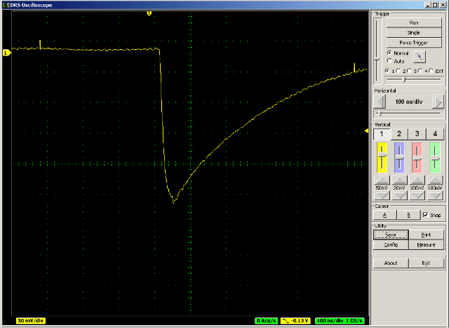
But when I open the binary file in IDL using:
data = uintarr(1024) ;unsigned integer array
readu,lun1,data
free_lun,lun1
close,lun1
;Convert bits to Volts
data=data*0.000015259-0.5
window,0,xs=512,ys=512
plot,data[*]
  I get: I get: 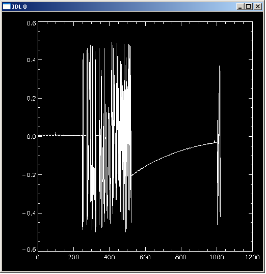
It looks like the pulse is there but there is something corrupting the data only in binary form. Is there a setting that may not be correct?
Thanks, Ron
|
|
36
|
Tue Feb 16 09:38:59 2010 |
Stefan Ritt | Problem reading oscilloscope binary waveform output |
| Ron Grazioso wrote: |
|
It looks like the pulse is there but there is something corrupting the data only in binary form. Is there a setting that may not be correct?
|
Yes, but you have to recompile the oscilloscope application. Find following line in the source file DOFrame.cpp:
m_WFfd = open(filename.char_str(), O_RDWR | O_CREAT | O_TRUNC | O_TEXT, 0644);
and replace it with
m_WFfd = open(filename.char_str(), O_RDWR | O_CREAT | O_TRUNC | O_BINARY, 0644);
that fixes the problem. To compile the program, you need MS Visual C++ and you have to install the vxWidgets library. Let me know if you have any problem with that.
Anyhow I plan a major software update soon (weeks), which not only fixes this problem, but also reduces the noise considerably by doing a kind of two-fold calibration.
- Stefan |
|
37
|
Sat Feb 20 01:56:05 2010 |
Hao Huan | PLLLCK signal of DRS4 | Hi Stefan,
in the latest DRS4 datasheet I only saw your data of the DRS4 PLL locking time for 6GSPS sampling speed, with other rows "TBD". Have you tried those lower frequencies? According to the datasheet I think the PLLLCK should be stabily low when the PLL is locked; am I right? However when I try my design with the DRS4 chip and feed the reference clock signal at 0.5MHz or 2MHz, the PLLLCK I get can never stabilize. There could be some problem in the PCB circuit connection, but I want to confirm with you since I'm confused with those "TBD" blanks.
Thanks a lot!
|
|
38
|
Sat Feb 20 09:54:48 2010 |
Stefan Ritt | PLLLCK signal of DRS4 |
| Hao Huan wrote: |
|
Hi Stefan,
in the latest DRS4 datasheet I only saw your data of the DRS4 PLL locking time for 6GSPS sampling speed, with other rows "TBD". Have you tried those lower frequencies? According to the datasheet I think the PLLLCK should be stabily low when the PLL is locked; am I right? However when I try my design with the DRS4 chip and feed the reference clock signal at 0.5MHz or 2MHz, the PLLLCK I get can never stabilize. There could be some problem in the PCB circuit connection, but I want to confirm with you since I'm confused with those "TBD" blanks.
Thanks a lot!
|
The locking time is typically 20-30 cycles of the external reference clock, I will update the numbers in the datasheet soon. I attached a screenshot of the chip when starting up at 1 GHz (0.5 MHz REFCLK), so you can see the behaviour. The upper curver is the DTAP signal, the lower curve the PLLLCK signal. As you can see, the PLLLCK signal is not purely digital. Actually it's a simple XOR between the REFCLK and the DTAP signal, so you need an external 4.7nF capacitor to "integrate" this signal. Without this capacitor, you would see small negative spikes whenever there is s small phase shift between the DTAP and the REFCLK signal. Have a look at your DTAP signal, is it in phase with the REFCLK? |
| Attachment 1: start_1ghz.png
|

|
|
39
|
Sun Feb 21 00:46:01 2010 |
Hao Huan | PLLLCK signal of DRS4 |
| Stefan Ritt wrote: |
|
| Hao Huan wrote: |
|
Hi Stefan,
in the latest DRS4 datasheet I only saw your data of the DRS4 PLL locking time for 6GSPS sampling speed, with other rows "TBD". Have you tried those lower frequencies? According to the datasheet I think the PLLLCK should be stabily low when the PLL is locked; am I right? However when I try my design with the DRS4 chip and feed the reference clock signal at 0.5MHz or 2MHz, the PLLLCK I get can never stabilize. There could be some problem in the PCB circuit connection, but I want to confirm with you since I'm confused with those "TBD" blanks.
Thanks a lot!
|
The locking time is typically 20-30 cycles of the external reference clock, I will update the numbers in the datasheet soon. I attached a screenshot of the chip when starting up at 1 GHz (0.5 MHz REFCLK), so you can see the behaviour. The upper curver is the DTAP signal, the lower curve the PLLLCK signal. As you can see, the PLLLCK signal is not purely digital. Actually it's a simple XOR between the REFCLK and the DTAP signal, so you need an external 4.7nF capacitor to "integrate" this signal. Without this capacitor, you would see small negative spikes whenever there is s small phase shift between the DTAP and the REFCLK signal. Have a look at your DTAP signal, is it in phase with the REFCLK?
|
Thanks! I see. The capacitor is important. However I'm a little confused... If PLLLCK=DTAP XOR REFCLK, shouldn't it integrate to low instead of high when the two clocks are in phase? I must have some misunderstanding here. So if we ignore any realistic complexity and assume DTAP is perfectly locked with REFCLK, will PLLLCK be always low or high? I'm sorry I do not know how the DRS internal PLL and its input/output work... |
|
40
|
Sun Feb 21 13:41:35 2010 |
Stefan Ritt | Real Time Conference 2010 | Hello,
may I draw your attention to the upcoming Real Time Conference 2010, taking place in Lisbon, Portugal, May 23rd to May 28th, 2010.
http://rt2010.ipfn.ist.utl.pt/
Several groups which are developing DRS4 electronics will come to this conference and present their work, so it will be a good opportunity to exchange ideas and experiences. There will also be a short course on digital pulse shape processing, which is highly relevant for our field.
Looking forward to see you in Lisbon,
Stefan |
|