| ID |
Date |
Author |
Subject |
|
370
|
Fri Sep 12 13:41:43 2014 |
Stefan Ritt | synchronizing two DRS4 evaluation boards readout with one computer |
| Dmitry Hits wrote: |
|
| Stefan Ritt wrote: |
|
| Dmitry Hits wrote: |
|
Hi everyone,
Has anyone tried to synchronize 2 (two) DRS4 evaluation boards readout by the same computer? I have read about some attempts on this board in the past, but I do not know if they have succeeded. If yes, could you share your experience and/or software.
Thank you very much,
Dmitry.
|
Please read the manual http://www.psi.ch/drs/DocumentationEN/manual_rev50.pdf page 25 where this is described in detail.
/Stefan
|
Hi Stefan,
Thank you for pointing me to the document. Does it apply only to version 5 of the board or can it be applied also to version 4 (which is the one I have)?
Dmitry
|
In principle it should also work with version 4, but I'm not sure how well the V4 software supports this. You might try the V5 software with your V4 boards.
/Stefan |
|
259
|
Fri Jun 7 11:44:17 2013 |
tmiron alon | thank you |
| Stefan Ritt wrote: |
|
| tmiron alon wrote: |
|
Hallo,
I'm using DRS4 Evaluation Board Rev 4.0 and I'm trying to change the output of the samples to be an average of # measurements (1000 or even more)
during the process I have encountered some difficulties I hope you will be able to help me with:
1. the DRS chip have 8 channels but the Evaluation board have only 4 channels. does the default mode of the DRS in the Evaluation Board is 1024 bins for each channel or 2048?
2. in the readout mode, does it samples all the 1024 bins waveform from a channel and then move to the next one, or after each bin it move to the next channel?
3. In the file "drs4_eval4_app.vhd", I have a problem finding the names of the signals that represents the registers bits which tell me what is the number of the bin (1-1024) the ADC is reading from the DRS, and the signals
that represents registers A0-A3. can you send me their names?
4. In another matter- is the -0.5V to 0.5V is the upper and lower limit of the input (or just a working range), and if not what is the limit for AC? is there a fuse on the board in case of overload from the input? (I didn't see it in the User's Manual, but I didn't know if you will mention it there in case there is one).
thanks in advance and have a nice day,
Tmiron
|
1. All 8 channels are read out, but only 4 are displayed in the oscilloscope.
2. It reads all 1024 bins from a channel, then switch to the next channel.
3. The ADC readout happens in lines 1576+. The register for the sample count is drs_sample_count, and the signal for the address is drs_addr.
4. The evaluation board manual explicitly mentions the maximum allowed input range on page 5.
/Stefan
|
Thank you for the answer.
Have a nice week,
Tmiron. |
|
542
|
Sun Oct 9 10:43:35 2016 |
Danny Petschke | time difference between 2 channels only ~30-35ps @ 5GSmples/s | (Board Type:9, DRS4)
Hello,
I´m trying to reach the timig resolution of about 2.5ps as written in the manual.
My settings are:
5GSamples/s
+/-0.5V
I followed the instructions of the manual. The chip was warm and ran about 10h. Then, Timing- followed by Voltage-Calibration.
The test-signal is a splittet sine-wave of 20MHz (function-generator) brought on A0 and A1 (A1 signal is delayed by 1ns-cable).
I´ve been testing different trigger-logic: (Chn1 AND Chn2), (Chn1 OR Chn2) and only Chn1 or Chn2.
Trigger-levels were changed too.
All setups show the same result of 1.009ns +/- 30-35ns (results from the DRS-Oscilloscope).
What is wrong from my side?
Thanks a lot for your help |
|
543
|
Sun Oct 9 11:39:18 2016 |
Stefan Ritt | time difference between 2 channels only ~30-35ps @ 5GSmples/s | Can you post a screenshot of your measurement?
Stefan
| Danny Petschke wrote: |
|
(Board Type:9, DRS4)
Hello,
I´m trying to reach the timig resolution of about 2.5ps as written in the manual.
My settings are:
5GSamples/s
+/-0.5V
I followed the instructions of the manual. The chip was warm and ran about 10h. Then, Timing- followed by Voltage-Calibration.
The test-signal is a splittet sine-wave of 20MHz (function-generator) brought on A0 and A1 (A1 signal is delayed by 1ns-cable).
I´ve been testing different trigger-logic: (Chn1 AND Chn2), (Chn1 OR Chn2) and only Chn1 or Chn2.
Trigger-levels were changed too.
All setups show the same result of 1.009ns +/- 30-35ns (results from the DRS-Oscilloscope).
What is wrong from my side?
Thanks a lot for your help
|
|
|
544
|
Mon Oct 10 11:30:37 2016 |
Danny Petschke | time difference between 2 channels only ~30-35ps @ 5GSmples/s | Hello Stefan,
Chn2 & Chn3 were used for delay-determination as you can see on the second picture.
The second picture shows all 4 Channels without any voltage input.
On Channel 4 streaks (red circle) occur often and Channel 1 has totally different Offset (Picture 1).
Thanks
| Stefan Ritt wrote: |
|
Can you post a screenshot of your measurement?
Stefan
| Danny Petschke wrote: |
|
(Board Type:9, DRS4)
Hello,
I´m trying to reach the timig resolution of about 2.5ps as written in the manual.
My settings are:
5GSamples/s
+/-0.5V
I followed the instructions of the manual. The chip was warm and ran about 10h. Then, Timing- followed by Voltage-Calibration.
The test-signal is a splittet sine-wave of 20MHz (function-generator) brought on A0 and A1 (A1 signal is delayed by 1ns-cable).
I´ve been testing different trigger-logic: (Chn1 AND Chn2), (Chn1 OR Chn2) and only Chn1 or Chn2.
Trigger-levels were changed too.
All setups show the same result of 1.009ns +/- 30-35ns (results from the DRS-Oscilloscope).
What is wrong from my side?
Thanks a lot for your help
|
|
|
|
545
|
Mon Oct 10 12:03:27 2016 |
Stefan Ritt | time difference between 2 channels only ~30-35ps @ 5GSmples/s | Ok, I got it. The timing resolution is affected by the signal-to-noise ratio over the rise-time of your signal. You find the full formula herer:
https://arxiv.org/abs/1405.4975
Your sine wave input signal has a slow rise time, and therefore limits the time resolution. I reproduced your measurement with a 20 MHz sine wave and got the same result:
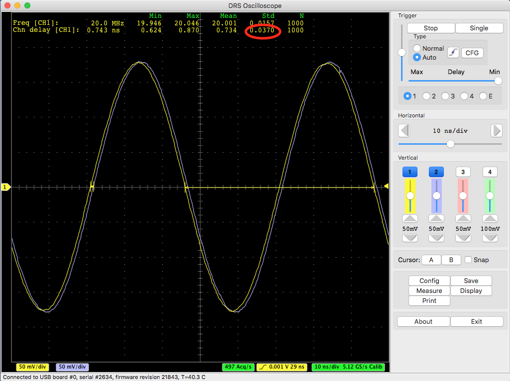
If I increase the frequency to 100 MHz and increase the amplitude, I get a better resolution:
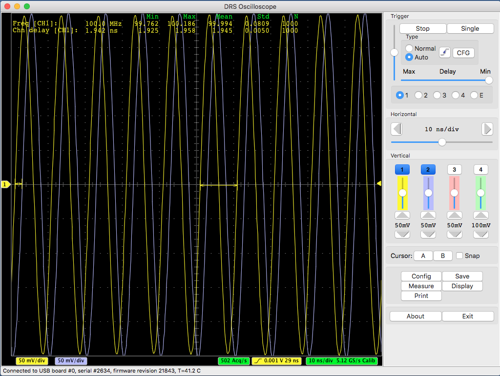
This is 5 ps which is better than 37 ps, but still not 2.5 ps. This can only be reached by sending single pulses to the evaluation board which have a rise time of > 300 mV / ns, which can be seen here:
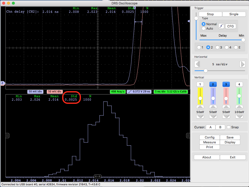
It is important to understand the relation timing - resolution vs. rise time / noise as explained in the quoted paper. If you have tiny pulses from your detector, you never will be able to measure excellent timing. This is physics, and not related to the specific electronics you are using.
Best regards,
Stefan
|
|
546
|
Tue Oct 11 09:04:33 2016 |
Danny Petschke | time difference between 2 channels only ~30-35ps @ 5GSmples/s | Hello Stefan,
thanks for the paper. That makes sense. I thought about sth. like that but wasn`t sure. Couldn´t check higher frequencies (limit of my function generator).
What do think about the other picture I attached yesterday where Chn1 shows a totally different offset than Chn2-4. Moreover Chn4 shows some streaks (red circle) ?
Best regards
Danny
| Stefan Ritt wrote: |
|
Ok, I got it. The timing resolution is affected by the signal-to-noise ratio over the rise-time of your signal. You find the full formula herer:
https://arxiv.org/abs/1405.4975
Your sine wave input signal has a slow rise time, and therefore limits the time resolution. I reproduced your measurement with a 20 MHz sine wave and got the same result:
If I increase the frequency to 100 MHz and increase the amplitude, I get a better resolution:
This is 5 ps which is better than 37 ps, but still not 2.5 ps. This can only be reached by sending single pulses to the evaluation board which have a rise time of > 300 mV / ns, which can be seen here:
It is important to understand the relation timing - resolution vs. rise time / noise as explained in the quoted paper. If you have tiny pulses from your detector, you never will be able to measure excellent timing. This is physics, and not related to the specific electronics you are using.
Best regards,
Stefan
|
|
|
547
|
Tue Oct 11 09:20:04 2016 |
Stefan Ritt | time difference between 2 channels only ~30-35ps @ 5GSmples/s | Concerning the offset, it looks to me like you moved the offset slider slider of channel 1 to a non-zero position. You see that from the marker at the very left side of the screen, where the yellow marker is at a different position as the others. Hint: a right-click on that slider sets it to zero. The little streak could be some kind of external noise.
| Danny Petschke wrote: |
|
Hello Stefan,
thanks for the paper. That makes sense. I thought about sth. like that but wasn`t sure. Couldn´t check higher frequencies (limit of my function generator).
What do think about the other picture I attached yesterday where Chn1 shows a totally different offset than Chn2-4. Moreover Chn4 shows some streaks (red circle) ?
Best regards
Danny
|
|
|
548
|
Tue Oct 11 22:11:26 2016 |
Stefan Ritt | time difference between 2 channels only ~30-35ps @ 5GSmples/s | Thank you very much! I will check it tomorrow!
-d
Concerning the offset, it looks to me like you moved the offset slider slider of channel 1 to a non-zero position. You see that from the marker at the very left side of the screen, where the yellow marker is at a different position as the others. Hint: a right-click on that slider sets it to zero. The little streak could be some kind of external noise.
| Danny Petschke wrote: |
|
Hello Stefan,
thanks for the paper. That makes sense. I thought about sth. like that but wasn`t sure. Couldn´t check higher frequencies (limit of my function generator).
What do think about the other picture I attached yesterday where Chn1 shows a totally different offset than Chn2-4. Moreover Chn4 shows some streaks (red circle) ?
Best regards
Danny
|
|
|
412
|
Wed May 13 09:31:18 2015 |
Chenfei Yang | transparent-mode voltage | Hello Mr. Stefan Ritt
For DRS4 differential inputs ranges form 500mV to 1100mV, with ROFS set to 1.55V, O_OFS set to 1.3V, the outputs of DRS4 is shown in the attachment.
The left part of the waveform,DRS4 works in transparent mode, and then the readout take place. The DMV of transparent mode is bigger then the readout mode, and that makes ADC sampling harder.How may I solve this problem?
Best wishes!
Chenfei Yang |
|
413
|
Wed May 13 09:45:51 2015 |
Stefan Ritt | transparent-mode voltage | The ROFS signal has no effect in the transparent mode, so you have to adjust O_OFS between sampling and transparent mode accordingly. Either use a DAC or two voltages with an analog switch.
| Chenfei Yang wrote: |
|
Hello Mr. Stefan Ritt
For DRS4 differential inputs ranges form 500mV to 1100mV, with ROFS set to 1.55V, O_OFS set to 1.3V, the outputs of DRS4 is shown in the attachment.
The left part of the waveform,DRS4 works in transparent mode, and then the readout take place. The DMV of transparent mode is bigger then the readout mode, and that makes ADC sampling harder.How may I solve this problem?
Best wishes!
Chenfei Yang
|
|
|
414
|
Wed May 13 09:55:09 2015 |
Chenfei Yang | transparent-mode voltage | Here's the problem. My external ADC has 2Vpp differtial input voltage range. And the common-mode voltage of the inputs need to be 1.3V. I cannot make both the transparent-output and the readout-output meet the ADC input requirement.
| Stefan Ritt wrote: |
|
The ROFS signal has no effect in the transparent mode, so you have to adjust O_OFS between sampling and transparent mode accordingly. Either use a DAC or two voltages with an analog switch.
| Chenfei Yang wrote: |
|
Hello Mr. Stefan Ritt
For DRS4 differential inputs ranges form 500mV to 1100mV, with ROFS set to 1.55V, O_OFS set to 1.3V, the outputs of DRS4 is shown in the attachment.
The left part of the waveform,DRS4 works in transparent mode, and then the readout take place. The DMV of transparent mode is bigger then the readout mode, and that makes ADC sampling harder.How may I solve this problem?
Best wishes!
Chenfei Yang
|
|
|
|
415
|
Wed May 13 10:16:40 2015 |
Stefan Ritt | transparent-mode voltage | I see your point. Actually I will soon have the same issue since we design right now a board with an AD9637 using the transparent mode. Which one are you using? The common mode range given in the datasheet is limited to guarantee optimal performance. But some ADCs allow a slightly bigger common mode range with reduced performance, but which might still be ok for some application. A "real" solution would be to put switchable level shifters between the DRS and the ADC, but that requires 8 additional chips which is bad. Alternative the ADC could pick up the signal not at the DRS output but at the DRS input, but that would aslo require additional chips for multiplexing. So unfortunately no perfect solution for that...
| Chenfei Yang wrote: |
|
Here's the problem. My external ADC has 2Vpp differtial input voltage range. And the common-mode voltage of the inputs need to be 1.3V. I cannot make both the transparent-output and the readout-output meet the ADC input requirement.
| Stefan Ritt wrote: |
|
The ROFS signal has no effect in the transparent mode, so you have to adjust O_OFS between sampling and transparent mode accordingly. Either use a DAC or two voltages with an analog switch.
| Chenfei Yang wrote: |
|
Hello Mr. Stefan Ritt
For DRS4 differential inputs ranges form 500mV to 1100mV, with ROFS set to 1.55V, O_OFS set to 1.3V, the outputs of DRS4 is shown in the attachment.
The left part of the waveform,DRS4 works in transparent mode, and then the readout take place. The DMV of transparent mode is bigger then the readout mode, and that makes ADC sampling harder.How may I solve this problem?
Best wishes!
Chenfei Yang
|
|
|
|
|
416
|
Wed May 13 10:27:43 2015 |
Chenfei Yang | transparent-mode voltage | I'm using an AD9252, 0.9V common mode voltage is suggested and I already use 8 un-switchable level shifters. Just as you said, this common mode range is recommended for optimum performance and the device can function over a wider range with reasonable performance. So I think I could adjust O_OFS to a minor level during transparent output.
| Stefan Ritt wrote: |
|
I see your point. Actually I will soon have the same issue since we design right now a board with an AD9637 using the transparent mode. Which one are you using? The common mode range given in the datasheet is limited to guarantee optimal performance. But some ADCs allow a slightly bigger common mode range with reduced performance, but which might still be ok for some application. A "real" solution would be to put switchable level shifters between the DRS and the ADC, but that requires 8 additional chips which is bad. Alternative the ADC could pick up the signal not at the DRS output but at the DRS input, but that would aslo require additional chips for multiplexing. So unfortunately no perfect solution for that...
| Chenfei Yang wrote: |
|
Here's the problem. My external ADC has 2Vpp differtial input voltage range. And the common-mode voltage of the inputs need to be 1.3V. I cannot make both the transparent-output and the readout-output meet the ADC input requirement.
| Stefan Ritt wrote: |
|
The ROFS signal has no effect in the transparent mode, so you have to adjust O_OFS between sampling and transparent mode accordingly. Either use a DAC or two voltages with an analog switch.
| Chenfei Yang wrote: |
|
Hello Mr. Stefan Ritt
For DRS4 differential inputs ranges form 500mV to 1100mV, with ROFS set to 1.55V, O_OFS set to 1.3V, the outputs of DRS4 is shown in the attachment.
The left part of the waveform,DRS4 works in transparent mode, and then the readout take place. The DMV of transparent mode is bigger then the readout mode, and that makes ADC sampling harder.How may I solve this problem?
Best wishes!
Chenfei Yang
|
|
|
|
|
|
417
|
Wed May 13 12:34:49 2015 |
Stefan Ritt | transparent-mode voltage | There might be a solution. How do you bias th input of the DRS4 chip? If you use a scheme as described in elog:84, you can bias DRS_IN+ and DRS_IN- as desired. Take for example a board input range of 0-1V. For a 0V input, you bias DRS_IN+ and DRS_IN- both with 0.9V. A 1V input signal then puts DRS_IN+ to 1.4V and DRS_IN-to 0.4 V. In the transparent mode, DRS_OUT+ = DRS_IN+ and DRS_OUT- = O-OFS - DRS_OUT+. So if you put O-OFS to 0.9V, you get for a 0V board input signal DRS_OUT- = 2*0.9V - DRS_OUT+ = 0.9V. So DRS_OUT+ = DRS_OUT- = 0.9 V which is in the middle of your ADC range.
If you do now a DRS readout, you need a ROFS of roughly 0.9V. For a 0V input, the storage capacitors have a zero differential voltage (DRS_IN+ = DRS_IN- = 0.8V), so DRS_OUT+ = (0.8V - 0.8V) + ROFS = 0.9V, and since you have O-OFS=0.9V, you will also get DRS_OUT- = 2*0.9V - DRS_OUT+ = 0.9V. So you ranges for transparent mode nad DRS readout mode will be roughly the same. |
|
418
|
Wed May 13 12:52:22 2015 |
Chenfei Yang | transparent-mode voltage | Yes. I use exactly the same scheme as you mentioned. I'll try your solution.
| Stefan Ritt wrote: |
|
There might be a solution. How do you bias th input of the DRS4 chip? If you use a scheme as described in elog:84, you can bias DRS_IN+ and DRS_IN- as desired. Take for example a board input range of 0-1V. For a 0V input, you bias DRS_IN+ and DRS_IN- both with 0.9V. A 1V input signal then puts DRS_IN+ to 1.4V and DRS_IN-to 0.4 V. In the transparent mode, DRS_OUT+ = DRS_IN+ and DRS_OUT- = O-OFS - DRS_OUT+. So if you put O-OFS to 0.9V, you get for a 0V board input signal DRS_OUT- = 2*0.9V - DRS_OUT+ = 0.9V. So DRS_OUT+ = DRS_OUT- = 0.9 V which is in the middle of your ADC range.
If you do now a DRS readout, you need a ROFS of roughly 0.9V. For a 0V input, the storage capacitors have a zero differential voltage (DRS_IN+ = DRS_IN- = 0.8V), so DRS_OUT+ = (0.8V - 0.8V) + ROFS = 0.9V, and since you have O-OFS=0.9V, you will also get DRS_OUT- = 2*0.9V - DRS_OUT+ = 0.9V. So you ranges for transparent mode nad DRS readout mode will be roughly the same.
|
|
|
419
|
Wed May 13 16:13:07 2015 |
Chenfei Yang | transparent-mode voltage | If using a ROFS of 0.9V, the input would not between 1.05V~2.05V better non-linearity area. Is that appropriate?
| Stefan Ritt wrote: |
|
There might be a solution. How do you bias th input of the DRS4 chip? If you use a scheme as described in elog:84, you can bias DRS_IN+ and DRS_IN- as desired. Take for example a board input range of 0-1V. For a 0V input, you bias DRS_IN+ and DRS_IN- both with 0.9V. A 1V input signal then puts DRS_IN+ to 1.4V and DRS_IN-to 0.4 V. In the transparent mode, DRS_OUT+ = DRS_IN+ and DRS_OUT- = O-OFS - DRS_OUT+. So if you put O-OFS to 0.9V, you get for a 0V board input signal DRS_OUT- = 2*0.9V - DRS_OUT+ = 0.9V. So DRS_OUT+ = DRS_OUT- = 0.9 V which is in the middle of your ADC range.
If you do now a DRS readout, you need a ROFS of roughly 0.9V. For a 0V input, the storage capacitors have a zero differential voltage (DRS_IN+ = DRS_IN- = 0.8V), so DRS_OUT+ = (0.8V - 0.8V) + ROFS = 0.9V, and since you have O-OFS=0.9V, you will also get DRS_OUT- = 2*0.9V - DRS_OUT+ = 0.9V. So you ranges for transparent mode nad DRS readout mode will be roughly the same.
|
|
|
420
|
Wed May 13 16:25:24 2015 |
Stefan Ritt | transparent-mode voltage | To get the good linearity, you need indeed ROFS = 1.05V. With a O-OFS of 0.9V, a zero input signal would give you DRS_OUT+=1.05V and DRS_OUT-=0.75V. I think this is till in the range of your ADC, right? So it's a tradeoff between linearity and available range. I do not know how nonlinear the DRS4 will be for ROFS < 1.05V, you have to try. If it's getting too bad, you still can correct for this off-line.
| Chenfei Yang wrote: |
|
If using a ROFS of 0.9V, the input would not between 1.05V~2.05V better non-linearity area. Is that appropriate?
| Stefan Ritt wrote: |
|
There might be a solution. How do you bias th input of the DRS4 chip? If you use a scheme as described in elog:84, you can bias DRS_IN+ and DRS_IN- as desired. Take for example a board input range of 0-1V. For a 0V input, you bias DRS_IN+ and DRS_IN- both with 0.9V. A 1V input signal then puts DRS_IN+ to 1.4V and DRS_IN-to 0.4 V. In the transparent mode, DRS_OUT+ = DRS_IN+ and DRS_OUT- = O-OFS - DRS_OUT+. So if you put O-OFS to 0.9V, you get for a 0V board input signal DRS_OUT- = 2*0.9V - DRS_OUT+ = 0.9V. So DRS_OUT+ = DRS_OUT- = 0.9 V which is in the middle of your ADC range.
If you do now a DRS readout, you need a ROFS of roughly 0.9V. For a 0V input, the storage capacitors have a zero differential voltage (DRS_IN+ = DRS_IN- = 0.8V), so DRS_OUT+ = (0.8V - 0.8V) + ROFS = 0.9V, and since you have O-OFS=0.9V, you will also get DRS_OUT- = 2*0.9V - DRS_OUT+ = 0.9V. So you ranges for transparent mode nad DRS readout mode will be roughly the same.
|
|
|
|
158
|
Tue Mar 20 16:23:33 2012 |
Martin Petriska | triger for measuring time between pulses in channels | I have two BaF2 detectors with PMT connected to Ch1 and Ch2. At this time Im using external triger module to start DRS4. My evalution board is version 3 so I have no possibility to trigger on two or more pulses occurence on different channels. But I have this idea, trigger with analog trigger on channel 1 (start detector) will start measurement on all channels. After that using FPGA inside EVM to look if some value in Ch2 is bigger as treshold value for example 0,5V and if yes then send data by USB to PC, if signal in Ch2 is lower then restart measurement and wait on triger in Ch1. This way I want to eliminate false data transfer throw USB. Is this possible to implement it into DRS4 evaluation board firmware ?
Thanks. |
|
159
|
Tue Mar 20 16:33:50 2012 |
Stefan Ritt | triger for measuring time between pulses in channels |
| Martin Petriska wrote: |
|
I have two BaF2 detectors with PMT connected to Ch1 and Ch2. At this time Im using external triger module to start DRS4. My evalution board is version 3 so I have no possibility to trigger on two or more pulses occurence on different channels. But I have this idea, trigger with analog trigger on channel 1 (start detector) will start measurement on all channels. After that using FPGA inside EVM to look if some value in Ch2 is bigger as treshold value for example 0,5V and if yes then send data by USB to PC, if signal in Ch2 is lower then restart measurement and wait on triger in Ch1. This way I want to eliminate false data transfer throw USB. Is this possible to implement it into DRS4 evaluation board firmware ?
Thanks.
|
It is muuuuch easier to upgrade to a V4 board!
Modification of firmware is not so easy. You have to learn and understand VHDL. Then, you have to add additional registers for this thresholds, which requires modification of the C library as well. The data inside the evaluation boards is not yet calibrated (this is only done on the C library), so you have an uncertainty of 30-40mV in this data. |
|