 Tue Jan 29 14:43:44 2019, Abaz Kryemadhi, ROOT Macro for data acquired with the newest software Tue Jan 29 14:43:44 2019, Abaz Kryemadhi, ROOT Macro for data acquired with the newest software
|
Hello,
Is there a root macro for decoding binary data acquired with the newest software for single board or multi-boards daisy chained?
Cheers,
Abaz |
 Wed Jan 30 17:08:58 2019, Stefan Ritt, ROOT Macro for data acquired with the newest software Wed Jan 30 17:08:58 2019, Stefan Ritt, ROOT Macro for data acquired with the newest software
|
This one elog:361 should still work.
Stefan
| Abaz Kryemadhi wrote: |
|
Hello,
Is there a root macro for decoding binary data acquired with the newest software for single board or multi-boards daisy chained?
Cheers,
Abaz
|
|
|
Wed Jan 30 06:51:37 2019, Saurabh Neema, DRS4 domino wave stability study
|
We have been using DRS4 IC in our design for quite some time and it is giving good performance.
Till now we were using Domino wave frequency as 1 GSPS by use of reference clock to DRS4 and internal PLL of DRS4. Recently we tried to use 4GSPS by modifying the reference clock.
What I have found that DRS4 domino wave is more stable at 4 GSPS as compared to 1 GSPS by doing the timing jitter analysis. I am not sure if it is the property of DRS4 IC to be having more stable domino wave at higher frequency (by design) or it is due to some external effects like PLL loop filter or any other on board parasitic effects.
Please share if anyone has done any study of DRS4 Domino wave stability at different sampling frequencies.
Thanks,
|
|
Wed Jan 30 08:02:25 2019, Stefan Ritt, DRS4 domino wave stability study
|
The Domino wave is most stable at 5 GSPS, slowly degrades down to 3-2 GSPS, and at 1GSPS gets some significant jitter. This is for internal reasons in the chip and cannot be compensated by the loop filter. It is therefore important to run it as fast as possible if you want to achieve best timing resolution. As a rule of thumb, the jitter at 5 GSPS is about 20-25 ps, and at 1 GSPS it is maybe 150 ps. If you require good timing resolution, you can use the 9th channel to sample a stable reference clock (100 MHz for example) and measure timing relative to that clock. This way you can bring down the resolution to a few ps at 5GSPS and to maybe 40 ps at 1 GSPS.
Stefan
| Saurabh Neema wrote: |
|
We have been using DRS4 IC in our design for quite some time and it is giving good performance.
Till now we were using Domino wave frequency as 1 GSPS by use of reference clock to DRS4 and internal PLL of DRS4. Recently we tried to use 4GSPS by modifying the reference clock.
What I have found that DRS4 domino wave is more stable at 4 GSPS as compared to 1 GSPS by doing the timing jitter analysis. I am not sure if it is the property of DRS4 IC to be having more stable domino wave at higher frequency (by design) or it is due to some external effects like PLL loop filter or any other on board parasitic effects.
Please share if anyone has done any study of DRS4 Domino wave stability at different sampling frequencies.
Thanks,
|
|
|
Thu Nov 8 11:44:35 2018, Davide Depaoli, Timing Issue
|
Hi,

We are using the DRS4 Evaluation Board as a digitizer in our laboratory.
We found a strange behavior in the saved files, more specifically the time difference between two consecutive points is not constant, also after the Timing Calibration.
As an example, I paste a piece of a xml file saved using the drsosc program, acquiring CH1 (open):

	---------------------------
	---[ START XML EXAMPLE ]---
	---------------------------

	<?xml version="1.0" encoding="ISO-8859-1"?>
	<!-- created by MXML on Thu Nov  8 11:13:27 2018 -->
	<DRSOSC>
	<Event>
	<Serial>1</Serial>
	<Time>2018/11/08 11:13:27.163</Time>
	<HUnit>ns</HUnit>
	<VUnit>mV</VUnit>
	<Board_2796>
	<Trigger_Cell>216</Trigger_Cell>
	<Scaler0>0</Scaler0>
	<CHN1>
	<Data>0.000,-1.0</Data>
	<Data>1.083,-1.0</Data>
	<Data>2.143,-1.0</Data>
	<Data>2.926,-1.0</Data>
	<Data>4.249,-0.1</Data>
	<Data>4.929,-0.6</Data>
	<Data>6.075,-0.4</Data>
	<Data>7.042,0.0</Data>
	<Data>8.299,0.2</Data>

	[...]

	-------------------------
	---[ END XML EXAMPLE ]---
	-------------------------

We found the same behavior saving events in the binary format, and then reading them with the read_binary.cpp

Is there a way to fix our issue?

Thanks a lot

Davide and Alessio |
|
Thu Nov 8 11:54:33 2018, Stefan Ritt, Timing Issue
|
That's not a bug, but a feature of the DRS4 chip. The time bins have different values by the properties of the chip. They are generated by a chain of inverters, which all have different propagation times. This delay is measured by the time calibration and then applied. If you want equidistant bins,
you have to interpolate your data points (linearly or by splines) and resample the signal. You can find more details in the DRS4 data sheet.

Best,
Stefan


> Hi,
>
> We are using the DRS4 Evaluation Board as a digitizer in our laboratory.
> We found a strange behavior in the saved files, more specifically the time difference between two consecutive points is not constant, also after the Timing Calibration.
> As an example, I paste a piece of a xml file saved using the drsosc program, acquiring CH1 (open):
>
> 	---------------------------
> 	---[ START XML EXAMPLE ]---
> 	---------------------------
>
> 	<?xml version="1.0" encoding="ISO-8859-1"?>
> 	<!-- created by MXML on Thu Nov  8 11:13:27 2018 -->
> 	<DRSOSC>
> 	<Event>
> 	<Serial>1</Serial>
> 	<Time>2018/11/08 11:13:27.163</Time>
> 	<HUnit>ns</HUnit>
> 	<VUnit>mV</VUnit>
> 	<Board_2796>
> 	<Trigger_Cell>216</Trigger_Cell>
> 	<Scaler0>0</Scaler0>
> 	<CHN1>
> 	<Data>0.000,-1.0</Data>
> 	<Data>1.083,-1.0</Data>
> 	<Data>2.143,-1.0</Data>
> 	<Data>2.926,-1.0</Data>
> 	<Data>4.249,-0.1</Data>
> 	<Data>4.929,-0.6</Data>
> 	<Data>6.075,-0.4</Data>
> 	<Data>7.042,0.0</Data>
> 	<Data>8.299,0.2</Data>
>
> 	[...]
>
> 	-------------------------
> 	---[ END XML EXAMPLE ]---
> 	-------------------------
>
> We found the same behavior saving events in the binary format, and then reading them with the read_binary.cpp
>
> Is there a way to fix our issue?
>
> Thanks a lot
>
> Davide and Alessio |
|
Thu Nov 8 12:02:34 2018, Davide Depaoli, Timing Issue
|
Thanks a lot for the quick response.
We will do as you suggest.

Best regards

Davide and Alessio

> That's not a bug, but a feature of the DRS4 chip. The time bins have different values by the properties of the chip. They are generated by a chain of inverters, which all have different
propagation times. This delay is measured by the time calibration and then applied. If you want equidistant bins,
> you have to interpolate your data points (linearly or by splines) and resample the signal. You can find more details in the DRS4 data sheet.
>
> Best,
> Stefan
>
>
> > Hi,
> >
> > We are using the DRS4 Evaluation Board as a digitizer in our laboratory.
> > We found a strange behavior in the saved files, more specifically the time difference between two consecutive points is not constant, also after the Timing Calibration.
> > As an example, I paste a piece of a xml file saved using the drsosc program, acquiring CH1 (open):
> >
> > 	---------------------------
> > 	---[ START XML EXAMPLE ]---
> > 	---------------------------
> >
> > 	<?xml version="1.0" encoding="ISO-8859-1"?>
> > 	<!-- created by MXML on Thu Nov  8 11:13:27 2018 -->
> > 	<DRSOSC>
> > 	<Event>
> > 	<Serial>1</Serial>
> > 	<Time>2018/11/08 11:13:27.163</Time>
> > 	<HUnit>ns</HUnit>
> > 	<VUnit>mV</VUnit>
> > 	<Board_2796>
> > 	<Trigger_Cell>216</Trigger_Cell>
> > 	<Scaler0>0</Scaler0>
> > 	<CHN1>
> > 	<Data>0.000,-1.0</Data>
> > 	<Data>1.083,-1.0</Data>
> > 	<Data>2.143,-1.0</Data>
> > 	<Data>2.926,-1.0</Data>
> > 	<Data>4.249,-0.1</Data>
> > 	<Data>4.929,-0.6</Data>
> > 	<Data>6.075,-0.4</Data>
> > 	<Data>7.042,0.0</Data>
> > 	<Data>8.299,0.2</Data>
> >
> > 	[...]
> >
> > 	-------------------------
> > 	---[ END XML EXAMPLE ]---
> > 	-------------------------
> >
> > We found the same behavior saving events in the binary format, and then reading them with the read_binary.cpp
> >
> > Is there a way to fix our issue?
> >
> > Thanks a lot
> >
> > Davide and Alessio |
Mon Nov 5 17:17:08 2018, Sean Quinn, Pi attenuator on eval board inputs? 
|
Dear DRS4 team,
I am curious about this part of the circuit:
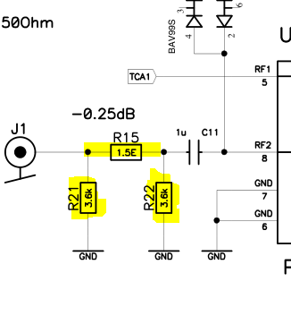
What is the purpose of this? |
|
Thu Nov 8 09:57:26 2018, Stefan Ritt, Pi attenuator on eval board inputs?
|
The attenuator compensates for the gain of the buffer which is slightly above one. In addition, it serves as a "placeholder" in case one wants larger input signals. One can easily convert the attenuator to -6db, -12db, etc. by chaning the resistors.
Stefan
| Sean Quinn wrote: |
|
Dear DRS4 team,
I am curious about this part of the circuit:
What is the purpose of this?
|
|
|
Sun Sep 23 02:22:46 2018, Gerard Arino-Estrada, Trigger OUT pulse width variable from 100 us up to 100 ms
|
Hello Stefan,
I am using the DRS4 board connected to a Raspberry PI and through the drsosc application. I am interested on using the "Trigger OUT" signal to do some extra data processing with NIM modules. According to the manual, for each hardware trigger a TTL pulse of 150 ns width should be send through the "trigger OUT". In my case I do see pulses with widths ranging from 100 microseconds up to hundreds of miliseconds. I am connecting the signal directly to an oscilloscope with 50 Ohm termination. I have tried two DRS4 boards in identical conditions and both show the same behavior. Having such wide and variable pulses makes it complicated for me to do the extra post-processing. Have you any idea of what might be going wrong? Thank you very much.
Best regards,
Gerard |
|
Wed Sep 26 14:44:14 2018, Stefan Ritt, Trigger OUT pulse width variable from 100 us up to 100 ms
|
The "Trigger OUT" has changed recently. It goes high on a new trigger, but then STAYS high until the board has been read out by the PC and re-started. This allows better synchronization with some external trigger, which can be re-armed with the falling edge of the trigger out signal. The signal can be quite long, since readout of an event via USB typically takes 2 ms, but can be more if the PC is busy. If you need back your 150 ns pulse, send the trigger out to an external pulse shaper with fixed shaping width.
Stefan
| Gerard Arino-Estrada wrote: |
|
Hello Stefan,
I am using the DRS4 board connected to a Raspberry PI and through the drsosc application. I am interested on using the "Trigger OUT" signal to do some extra data processing with NIM modules. According to the manual, for each hardware trigger a TTL pulse of 150 ns width should be send through the "trigger OUT". In my case I do see pulses with widths ranging from 100 microseconds up to hundreds of miliseconds. I am connecting the signal directly to an oscilloscope with 50 Ohm termination. I have tried two DRS4 boards in identical conditions and both show the same behavior. Having such wide and variable pulses makes it complicated for me to do the extra post-processing. Have you any idea of what might be going wrong? Thank you very much.
Best regards,
Gerard
|
|
|
Wed Sep 26 18:28:20 2018, Gerard Arino-Estrada, Trigger OUT pulse width variable from 100 us up to 100 ms
|
Thank you very much for the answer, I really appreciate your help.
Thanks!
Gerard
| Stefan Ritt wrote: |
|
The "Trigger OUT" has changed recently. It goes high on a new trigger, but then STAYS high until the board has been read out by the PC and re-started. This allows better synchronization with some external trigger, which can be re-armed with the falling edge of the trigger out signal. The signal can be quite long, since readout of an event via USB typically takes 2 ms, but can be more if the PC is busy. If you need back your 150 ns pulse, send the trigger out to an external pulse shaper with fixed shaping width.
Stefan
| Gerard Arino-Estrada wrote: |
|
Hello Stefan,
I am using the DRS4 board connected to a Raspberry PI and through the drsosc application. I am interested on using the "Trigger OUT" signal to do some extra data processing with NIM modules. According to the manual, for each hardware trigger a TTL pulse of 150 ns width should be send through the "trigger OUT". In my case I do see pulses with widths ranging from 100 microseconds up to hundreds of miliseconds. I am connecting the signal directly to an oscilloscope with 50 Ohm termination. I have tried two DRS4 boards in identical conditions and both show the same behavior. Having such wide and variable pulses makes it complicated for me to do the extra post-processing. Have you any idea of what might be going wrong? Thank you very much.
Best regards,
Gerard
|
|
|
|
Wed Sep 26 19:21:03 2018, Stefan Ritt, Trigger OUT pulse width variable from 100 us up to 100 ms
|
In meantime I even updated the manual.
Stefan
| Gerard Arino-Estrada wrote: |
|
Thank you very much for the answer, I really appreciate your help.
Thanks!
Gerard
|
|
|
Thu May 17 13:29:34 2018, Stefan Ritt, "Symmetric spikes" fixed
|
Good news for all DRS4 users. After many years, I finally understand where the "symmetric spikes" come from and how to fix them.
The "symmetric spikes" are small spikes of 17-18mV, which randomly happen at 1-2 cells. They alwas come in groups of 2 in each channel, symmetric around sampling cell #512. See first attachment.
The reason for the spikes is the previous readout cycle. On each readout cycle, the "read bit" is clocked through all 1024 cells to switch one cell contents to the DRS4 output. At the end of the 1024 cycles, the read bit stays at its last position. The bit is carried by a metal line on the chip, which crosses all 9 channels (second attachment). This bit now influences the sampling cells below the metal line capacitively, so their contents is "pushed up" by a few mV, just like the ROFS offset does. Since the DRS sampling channels are in a snake layout, going 0-512 from left, then 512-1023 back again, the line crosses two cells in each channel, and thus the symmetric spikes.
Previously, there was a software solution for that. In the evaluation board software DRSOsc there is a button "Remove spikes" which tries to fix this in software. Although this works most of the time, it's annoying and not 100% safe. Like when the spike sits on top of a noise signal, it might not be recognized. Fixing this in hardware is however straight forwar. After the readout cycle ends, push the read bit out of the chip:
- Address the read shift register by applying 1011b to A3:A0
- Switch SRIN low
- Apply 1024 clock cycles to SRCLK
This shifts the bit out of the chip, so that the next event is not affected by the read bit. The third attachment show the effect of this. The "clear cycle" increases the readout time a little bit, but depending on the application this might be worth it.
Regards,
Stefan |
|
Mon Sep 3 11:17:26 2018, Martin Petriska, "Symmetric spikes" fixed
|
Hi,
Is it possible to fix it by FPGA changes? I see readout cycle (proc_drs_reedout) in drs4_eval(4)5_app.vhd, but not sure where to exactly put this three commands. Could you please attach app.vhd file for eval board with example how to fix ?
Regards,
Martin
| Stefan Ritt wrote: |
|
Good news for all DRS4 users. After many years, I finally understand where the "symmetric spikes" come from and how to fix them.
The "symmetric spikes" are small spikes of 17-18mV, which randomly happen at 1-2 cells. They alwas come in groups of 2 in each channel, symmetric around sampling cell #512. See first attachment.
The reason for the spikes is the previous readout cycle. On each readout cycle, the "read bit" is clocked through all 1024 cells to switch one cell contents to the DRS4 output. At the end of the 1024 cycles, the read bit stays at its last position. The bit is carried by a metal line on the chip, which crosses all 9 channels (second attachment). This bit now influences the sampling cells below the metal line capacitively, so their contents is "pushed up" by a few mV, just like the ROFS offset does. Since the DRS sampling channels are in a snake layout, going 0-512 from left, then 512-1023 back again, the line crosses two cells in each channel, and thus the symmetric spikes.
Previously, there was a software solution for that. In the evaluation board software DRSOsc there is a button "Remove spikes" which tries to fix this in software. Although this works most of the time, it's annoying and not 100% safe. Like when the spike sits on top of a noise signal, it might not be recognized. Fixing this in hardware is however straight forwar. After the readout cycle ends, push the read bit out of the chip:
- Address the read shift register by applying 1011b to A3:A0
- Switch SRIN low
- Apply 1024 clock cycles to SRCLK
This shifts the bit out of the chip, so that the next event is not affected by the read bit. The third attachment show the effect of this. The "clear cycle" increases the readout time a little bit, but depending on the application this might be worth it.
Regards,
Stefan
|
|
|
Tue Sep 4 13:04:30 2018, Stefan Ritt, "Symmetric spikes" fixed
|
Yes it's possible, but I have to find time for that. The software of the evaluation board takes care of the spikes ("remove spikes"), so I thought it's not so urgent to fix that in the FPGA (which takes me some time).
Stefan
| Martin Petriska wrote: |
|
Hi,
Is it possible to fix it by FPGA changes? I see readout cycle (proc_drs_reedout) in drs4_eval(4)5_app.vhd, but not sure where to exactly put this three commands. Could you please attach app.vhd file for eval board with example how to fix ?
Regards,
Martin
| Stefan Ritt wrote: |
|
Good news for all DRS4 users. After many years, I finally understand where the "symmetric spikes" come from and how to fix them.
The "symmetric spikes" are small spikes of 17-18mV, which randomly happen at 1-2 cells. They alwas come in groups of 2 in each channel, symmetric around sampling cell #512. See first attachment.
The reason for the spikes is the previous readout cycle. On each readout cycle, the "read bit" is clocked through all 1024 cells to switch one cell contents to the DRS4 output. At the end of the 1024 cycles, the read bit stays at its last position. The bit is carried by a metal line on the chip, which crosses all 9 channels (second attachment). This bit now influences the sampling cells below the metal line capacitively, so their contents is "pushed up" by a few mV, just like the ROFS offset does. Since the DRS sampling channels are in a snake layout, going 0-512 from left, then 512-1023 back again, the line crosses two cells in each channel, and thus the symmetric spikes.
Previously, there was a software solution for that. In the evaluation board software DRSOsc there is a button "Remove spikes" which tries to fix this in software. Although this works most of the time, it's annoying and not 100% safe. Like when the spike sits on top of a noise signal, it might not be recognized. Fixing this in hardware is however straight forwar. After the readout cycle ends, push the read bit out of the chip:
- Address the read shift register by applying 1011b to A3:A0
- Switch SRIN low
- Apply 1024 clock cycles to SRCLK
This shifts the bit out of the chip, so that the next event is not affected by the read bit. The third attachment show the effect of this. The "clear cycle" increases the readout time a little bit, but depending on the application this might be worth it.
Regards,
Stefan
|
|
|
|
Thu Sep 13 18:09:13 2018, Martin Petriska, "Symmetric spikes" fixed
|
Ok, so I made it ... and Yes it works :),
https://youtu.be/0noy4CoFoh8
here is changed part in drs4_eval4_app.vhd
        when done =>

          drs_readout_state    <= spikeoff;

          drs_stat_busy        <= '0';

          drs_dpram_we1        <= '0';

          drs_write_set        <= '1';   -- set drs_write_ff in proc_drs_write

                                         -- to keep chip "warm"
 -- spike fix ELOG 697


          when spikeoff =>

            o_drs_addr       <= "1011"; -- Address the read shift register by applying 1011b to A3:A0

            o_drs_srin       <= '0'; -- Switch SRIN low

             drs_readout_state                 <= spikecycle;

             -- Apply 1024 clock cycles to SRCLK

             drs_sr_count         <= 0;
          when spikecycle =>

             drs_sr_count         <= drs_sr_count + 1;

             o_drs_srclk          <= not o_drs_srclk;

             if (drs_sr_count = 1024) then

                drs_readout_state <= idle;

             end if;
-- set-up of configuration register
| Stefan Ritt wrote: |
|
Yes it's possible, but I have to find time for that. The software of the evaluation board takes care of the spikes ("remove spikes"), so I thought it's not so urgent to fix that in the FPGA (which takes me some time).
Stefan
| Martin Petriska wrote: |
|
Hi,
Is it possible to fix it by FPGA changes? I see readout cycle (proc_drs_reedout) in drs4_eval(4)5_app.vhd, but not sure where to exactly put this three commands. Could you please attach app.vhd file for eval board with example how to fix ?
Regards,
Martin
| Stefan Ritt wrote: |
|
Good news for all DRS4 users. After many years, I finally understand where the "symmetric spikes" come from and how to fix them.
The "symmetric spikes" are small spikes of 17-18mV, which randomly happen at 1-2 cells. They alwas come in groups of 2 in each channel, symmetric around sampling cell #512. See first attachment.
The reason for the spikes is the previous readout cycle. On each readout cycle, the "read bit" is clocked through all 1024 cells to switch one cell contents to the DRS4 output. At the end of the 1024 cycles, the read bit stays at its last position. The bit is carried by a metal line on the chip, which crosses all 9 channels (second attachment). This bit now influences the sampling cells below the metal line capacitively, so their contents is "pushed up" by a few mV, just like the ROFS offset does. Since the DRS sampling channels are in a snake layout, going 0-512 from left, then 512-1023 back again, the line crosses two cells in each channel, and thus the symmetric spikes.
Previously, there was a software solution for that. In the evaluation board software DRSOsc there is a button "Remove spikes" which tries to fix this in software. Although this works most of the time, it's annoying and not 100% safe. Like when the spike sits on top of a noise signal, it might not be recognized. Fixing this in hardware is however straight forwar. After the readout cycle ends, push the read bit out of the chip:
- Address the read shift register by applying 1011b to A3:A0
- Switch SRIN low
- Apply 1024 clock cycles to SRCLK
This shifts the bit out of the chip, so that the next event is not affected by the read bit. The third attachment show the effect of this. The "clear cycle" increases the readout time a little bit, but depending on the application this might be worth it.
Regards,
Stefan
|
|
|
|
|
Wed Aug 1 00:49:30 2018, Sean Quinn, Optimal readout speed
|
Dear DRS4 team,
On page 3 of the data sheet, Table 1. for readout speed a typical value of 10 MHz is specified, but in the comment column it notes optimal performance achieved at 33 MHz.
I see the V5.1 eval board runs at 16 MHz. I'd like to understand the rationale for this using speed, instead of 33 MHz. Is there an SNR issue for the ADC at the higher speed, even though this is optimal for the DRS4?
Very best,
Sean |
|
Tue Aug 21 14:36:44 2018, Stefan Ritt, Optimal readout speed
|
The analog output of the DRS4 chip needs some time to settle. In principle it need an infinite amout of time (exponential curve) to settle to 100% of the final value. So if we sample after a finite time, there is some error we do. Some of the error will be taken care of the voltage calibration, but there remains some residual error depending on the value of the previous sampling cell. So all sampling speeds 10 MHz, 16 MHz, 33 MHz are kind of rule of thumbs. In the end we run the evaluation board at 16 MHz to save a little bit of power (which is limited on an USB device). But I never made a careful study of noise-after-calibration vs. sampling speed. If you have some measurements, I'm happt to include it in the data sheet.
Stefan
| Sean Quinn wrote: |
|
Dear DRS4 team,
On page 3 of the data sheet, Table 1. for readout speed a typical value of 10 MHz is specified, but in the comment column it notes optimal performance achieved at 33 MHz.
I see the V5.1 eval board runs at 16 MHz. I'd like to understand the rationale for this using speed, instead of 33 MHz. Is there an SNR issue for the ADC at the higher speed, even though this is optimal for the DRS4?
Very best,
Sean
|
|
|
Mon Aug 13 19:44:59 2018, Martin Petriska, Latch delay support
|
Hi,
https://forge.physik.rwth-aachen.de/projects/drs4-rwth
Not sure about their licensing, but is it possible to add latch delay support to official firmware ?
Best regards
Martin |
|
Tue Aug 14 06:10:49 2018, Stefan Ritt, Latch delay support
|
I put that on the wish list, but I won't have time for that in the next months.
Stefan
| Martin Petriska wrote: |
|
Hi,
https://forge.physik.rwth-aachen.de/projects/drs4-rwth
Not sure about their licensing, but is it possible to add latch delay support to official firmware ?
Best regards
Martin
|
|
|
Mon Jul 16 19:39:35 2018, Woon-Seng Choong, Effect of interpolation on timing
|
Using a test pulse split into two channels of the DRS4 Evaluation Board v5, I looked at the time resolution using a leading edge threshold. The voltage and timing calibration was performed. One method (1) is to linearly interpolate between two points of the raw waveform that is above and below the threshold (this is exactly the algorithm given in read_binary.c in the drs4 source distribution); and another (2) is to use a cubic spline interpolation of the raw waveform. The results I obtained are:
Method 1: dt = 1.298 ns +/- 7.22 ps
Method 2: dt = 1.293 ns +/- 15.48 ps
I am really puzzled why the time resolution of the spline interpolation is about a factor 2 worse than the simple linear interpolation. Has anyone studied the time resolution using similar or other interpolation methods?
|
|
Fri Jul 20 00:44:13 2018, Woon-Seng Choong, Effect of interpolation on timing
|
Just a follow-up update.
It turns out that I was using a cubic spline interpolation with smoothing. If I required the cubic spline to go through the sampled points, then I obtained similar time resolution as the simple linear interpolation.
| Woon-Seng Choong wrote: |
|
Using a test pulse split into two channels of the DRS4 Evaluation Board v5, I looked at the time resolution using a leading edge threshold. The voltage and timing calibration was performed. One method (1) is to linearly interpolate between two points of the raw waveform that is above and below the threshold (this is exactly the algorithm given in read_binary.c in the drs4 source distribution); and another (2) is to use a cubic spline interpolation of the raw waveform. The results I obtained are:
Method 1: dt = 1.298 ns +/- 7.22 ps
Method 2: dt = 1.293 ns +/- 15.48 ps
I am really puzzled why the time resolution of the spline interpolation is about a factor 2 worse than the simple linear interpolation. Has anyone studied the time resolution using similar or other interpolation methods?
|
|
|
Thu Jun 28 19:55:45 2018, Woon-Seng Choong, Negative Bin Width
|
I am using a DRS4 Evaluation Board v5 and running the drsosc.exe version 5.06 on a Window 7 machine. I have performed the voltage and timing calibration.
With test pulses on channel 1 and 2, I collected binary data file with all 4 channels active sampling at 5GSPS.
Attached is a distribution of the bin_width vs. cell # for all the 4 channels. Note that there are few cells with bin_width < 10 ps.
Channel 1: bin_width[498] = -0.000348, bin_width[1010]= -0.000348
Channel 2: bin_width[498] = 0.007363
Channel 3: bin_width[498] = 0.007843
Channel 4: bin_width[498] = 0.005948
Is this normal? How can you get negative bin_width? What does negative bin_width means?
I have attached the binary data file for your verification.
|
|
Fri Jun 29 07:51:33 2018, Stefan Ritt, Negative Bin Width
|
Yes that's normal. A negative cell bin width means that the next cell N+1 samples the input signal before cell N. This can happen due to the signal routing on the DRS4 chip.
Stefan
| Woon-Seng Choong wrote: |
|
I am using a DRS4 Evaluation Board v5 and running the drsosc.exe version 5.06 on a Window 7 machine. I have performed the voltage and timing calibration.
With test pulses on channel 1 and 2, I collected binary data file with all 4 channels active sampling at 5GSPS.
Attached is a distribution of the bin_width vs. cell # for all the 4 channels. Note that there are few cells with bin_width < 10 ps.
Channel 1: bin_width[498] = -0.000348, bin_width[1010]= -0.000348
Channel 2: bin_width[498] = 0.007363
Channel 3: bin_width[498] = 0.007843
Channel 4: bin_width[498] = 0.005948
Is this normal? How can you get negative bin_width? What does negative bin_width means?
I have attached the binary data file for your verification.
|
|
|
Tue Jun 19 06:42:23 2018, Phan Van Chuan, The data acquisition speed
|
Dear Stefan,
We are using an DRS4 board V5.1 for building a metering system for the scintillator detector by a Labview program. The program was built based on the functions in DRS.cpp and it reads data from channel 0 very well (Fig 1). Now, I am having a problem with the data acquisition from DRS4 board. The data acquisition speed on this program is only about 30-50 Acq / s, while using the DRS Oscilloscope that of about 300-400 Acq / s.
When the program was installed with fDominoMode = 0 and fDominoActive = 0, the data acquisition speed was about 300-400 Acq / s. However, the waveform is inaccurate.
I do not know if I installed the wrong function! Can you show me how to solve this problem?
In the Labview program, functions (corresponding to functions in DRS.cpp) are called with the following parameters:
InitFPGA();
SetMultiBuffer(0);
fROFS = 1.6; // differential input range -0.5V ... +0.5V
fRange = 0;
SetDAC(fDAC_ROFS_1, fROFS);
fCommonMode = 0.8; // 0.8V +- 0.5V inside NMOS range
SetDAC(fDAC_CALP, fCommonMode);
SetDAC(fDAC_CALN, fCommonMode);
SetDAC(fDAC_BIAS, 0.70);
/* set default number of channels per chip */
SetChannelConfig(0, fNumberOfReadoutChannels - 1, 8);
// set ADC clock phase
fADCClkPhase = 0;
fADCClkInvert = 0;
// default settings
fMultiBuffer = 0;
fNMultiBuffer = 0;
fDominoMode = 1;
fReadoutMode = 1;
fReadPointer = 0;
fTriggerEnable1 = 1;
fTriggerEnable2 = 0;
fTriggerSource = 0;
fTriggerDelay = 0;
fTriggerDelayNs = 0;
fSyncDelay = 0;
fNominalFrequency = 1;
fDominoActive = 1;
// load calibration from EEPROM
ReadCalibration();
...
SetDominoMode(fDominoMode);
SetReadoutMode(fReadoutMode);
EnableTrigger(fTriggerEnable1, fTriggerEnable2);
SetTriggerSource(fTriggerSource);
SetTriggerDelayPercent(0);
SetSyncDelay(fSyncDelay);
SetDominoActive(fDominoActive);
SetFrequency(fNominalFrequency, true);
SetInputRange(fRange);
SelectClockSource(0); // FPGA clock
// disable calibration signals
EnableAcal(0, 0);
SetCalibTiming(0, 0);
EnableTcal(0);
// got to idle state
Reinit();
////////
SetFrequency (1,false);
settranspmode (1);
setinputrange(0);
EnableTcal (0,-,-);
EnableTrigger(1, 0);
SetTriggerSource(0);
SetTriggerLevel(0);
SetTriggerPolarity(false);
SetTriggerDelayNs(512);
// in loop of read data from DRS4:
{
StartDomino();
while (b->IsBusy());
TransferWaves(0, 8);
GetTime(0, 0, b->GetTriggerCell(0), time_array[0]);
GetWave(0, 0, wave_array[0]);
}
Thank you very much!
Best Regards,
Chuan
|
|
Tue Jun 19 10:05:50 2018, Stefan Ritt, The data acquisition speed
|
How do you tigger the board? In your code below you start the board (StartDomino()) and then wait for a trigger. Setting the trigger level to zero (via SetTriggerLevel(0)) is certainly wrong. Please have a look at drs_exam.cpp in the distribution and use the same functions used there. If you want to trigger the board, you need some external pulser with high enough rate (more than 500 Hz or course). You can also "software" trigger the board with a call to SoftTrigger() just after StartDomino(). This is then like the "auto" trigger on an oscilloscope.
Stefan
| Phan Van Chuan wrote: |
|
Dear Stefan,
We are using an DRS4 board V5.1 for building a metering system for the scintillator detector by a Labview program. The program was built based on the functions in DRS.cpp and it reads data from channel 0 very well (Fig 1). Now, I am having a problem with the data acquisition from DRS4 board. The data acquisition speed on this program is only about 30-50 Acq / s, while using the DRS Oscilloscope that of about 300-400 Acq / s.
When the program was installed with fDominoMode = 0 and fDominoActive = 0, the data acquisition speed was about 300-400 Acq / s. However, the waveform is inaccurate.
I do not know if I installed the wrong function! Can you show me how to solve this problem?
In the Labview program, functions (corresponding to functions in DRS.cpp) are called with the following parameters:
InitFPGA();
SetMultiBuffer(0);
fROFS = 1.6; // differential input range -0.5V ... +0.5V
fRange = 0;
SetDAC(fDAC_ROFS_1, fROFS);
fCommonMode = 0.8; // 0.8V +- 0.5V inside NMOS range
SetDAC(fDAC_CALP, fCommonMode);
SetDAC(fDAC_CALN, fCommonMode);
SetDAC(fDAC_BIAS, 0.70);
/* set default number of channels per chip */
SetChannelConfig(0, fNumberOfReadoutChannels - 1, 8);
// set ADC clock phase
fADCClkPhase = 0;
fADCClkInvert = 0;
// default settings
fMultiBuffer = 0;
fNMultiBuffer = 0;
fDominoMode = 1;
fReadoutMode = 1;
fReadPointer = 0;
fTriggerEnable1 = 1;
fTriggerEnable2 = 0;
fTriggerSource = 0;
fTriggerDelay = 0;
fTriggerDelayNs = 0;
fSyncDelay = 0;
fNominalFrequency = 1;
fDominoActive = 1;
// load calibration from EEPROM
ReadCalibration();
...
SetDominoMode(fDominoMode);
SetReadoutMode(fReadoutMode);
EnableTrigger(fTriggerEnable1, fTriggerEnable2);
SetTriggerSource(fTriggerSource);
SetTriggerDelayPercent(0);
SetSyncDelay(fSyncDelay);
SetDominoActive(fDominoActive);
SetFrequency(fNominalFrequency, true);
SetInputRange(fRange);
SelectClockSource(0); // FPGA clock
// disable calibration signals
EnableAcal(0, 0);
SetCalibTiming(0, 0);
EnableTcal(0);
// got to idle state
Reinit();
////////
SetFrequency (1,false);
settranspmode (1);
setinputrange(0);
EnableTcal (0,-,-);
EnableTrigger(1, 0);
SetTriggerSource(0);
SetTriggerLevel(0);
SetTriggerPolarity(false);
SetTriggerDelayNs(512);
// in loop of read data from DRS4:
{
StartDomino();
while (b->IsBusy());
TransferWaves(0, 8);
GetTime(0, 0, b->GetTriggerCell(0), time_array[0]);
GetWave(0, 0, wave_array[0]);
}
Thank you very much!
Best Regards,
Chuan
|
|
|
Tue Jun 19 12:54:51 2018, Phan Van Chuan, The data acquisition speed
|
Thank Stefan Ritt, I added the SoftTrigger() just after StartDomino(), so now, The data acquisition speed the same speed as in the DRS oscilloscope. I have misunderstood the "auto" trigger on an oscilloscope as setting SetTriggerLevel (0).
Thank so much!
Phan Van Chuan
| Phan Van Chuan wrote: |
|
Dear Stefan,
We are using an DRS4 board V5.1 for building a metering system for the scintillator detector by a Labview program. The program was built based on the functions in DRS.cpp and it reads data from channel 0 very well (Fig 1). Now, I am having a problem with the data acquisition from DRS4 board. The data acquisition speed on this program is only about 30-50 Acq / s, while using the DRS Oscilloscope that of about 300-400 Acq / s.
When the program was installed with fDominoMode = 0 and fDominoActive = 0, the data acquisition speed was about 300-400 Acq / s. However, the waveform is inaccurate.
I do not know if I installed the wrong function! Can you show me how to solve this problem?
In the Labview program, functions (corresponding to functions in DRS.cpp) are called with the following parameters:
InitFPGA();
SetMultiBuffer(0);
fROFS = 1.6; // differential input range -0.5V ... +0.5V
fRange = 0;
SetDAC(fDAC_ROFS_1, fROFS);
fCommonMode = 0.8; // 0.8V +- 0.5V inside NMOS range
SetDAC(fDAC_CALP, fCommonMode);
SetDAC(fDAC_CALN, fCommonMode);
SetDAC(fDAC_BIAS, 0.70);
/* set default number of channels per chip */
SetChannelConfig(0, fNumberOfReadoutChannels - 1, 8);
// set ADC clock phase
fADCClkPhase = 0;
fADCClkInvert = 0;
// default settings
fMultiBuffer = 0;
fNMultiBuffer = 0;
fDominoMode = 1;
fReadoutMode = 1;
fReadPointer = 0;
fTriggerEnable1 = 1;
fTriggerEnable2 = 0;
fTriggerSource = 0;
fTriggerDelay = 0;
fTriggerDelayNs = 0;
fSyncDelay = 0;
fNominalFrequency = 1;
fDominoActive = 1;
// load calibration from EEPROM
ReadCalibration();
...
SetDominoMode(fDominoMode);
SetReadoutMode(fReadoutMode);
EnableTrigger(fTriggerEnable1, fTriggerEnable2);
SetTriggerSource(fTriggerSource);
SetTriggerDelayPercent(0);
SetSyncDelay(fSyncDelay);
SetDominoActive(fDominoActive);
SetFrequency(fNominalFrequency, true);
SetInputRange(fRange);
SelectClockSource(0); // FPGA clock
// disable calibration signals
EnableAcal(0, 0);
SetCalibTiming(0, 0);
EnableTcal(0);
// got to idle state
Reinit();
////////
SetFrequency (1,false);
settranspmode (1);
setinputrange(0);
EnableTcal (0,-,-);
EnableTrigger(1, 0);
SetTriggerSource(0);
SetTriggerLevel(0);
SetTriggerPolarity(false);
SetTriggerDelayNs(512);
// in loop of read data from DRS4:
{
StartDomino();
while (b->IsBusy());
TransferWaves(0, 8);
GetTime(0, 0, b->GetTriggerCell(0), time_array[0]);
GetWave(0, 0, wave_array[0]);
}
Thank you very much!
Best Regards,
Chuan
|
|
|
Wed Jun 13 13:23:17 2018, Julian Kemp, Maximum analog input voltage
|
Dear all,
I have been wondering what the maximum analog input voltage for the DRS4 V5 evaluation board is. It came with a sticker indicating that it is "2.5V pk Max". On the other hand, when checking the manual (https://www.psi.ch/drs/DocumentationEN/manual_rev50.pdf), it says maximum allowed is 10V DC or even 30V for short pulses. I foresee an application where I cannot make sure that pulses stay below 2.5V, so the correct value will be quite important for me.
Best,
Julian |
|
Wed Jun 13 13:42:47 2018, Stefan Ritt, Maximum analog input voltage
|
In principle the numbers in the manual are correct. But they relate to pulses of a certain length, because the input protection only works for DC voltage and for pulses which are not too long. Since we could not write this all on the label of the board, we decided to put there 100% safe value as a "warning" to people, meaning that if pulses are above 2.5V, they should look into the manual and read the details.
Stefan
| Julian Kemp wrote: |
|
Dear all,
I have been wondering what the maximum analog input voltage for the DRS4 V5 evaluation board is. It came with a sticker indicating that it is "2.5V pk Max". On the other hand, when checking the manual (https://www.psi.ch/drs/DocumentationEN/manual_rev50.pdf), it says maximum allowed is 10V DC or even 30V for short pulses. I foresee an application where I cannot make sure that pulses stay below 2.5V, so the correct value will be quite important for me.
Best,
Julian
|
|
|
Wed Jun 13 16:34:28 2018, Julian Kemp, Maximum analog input voltage
|
Thank you! That solves my problem.
| Stefan Ritt wrote: |
|
In principle the numbers in the manual are correct. But they relate to pulses of a certain length, because the input protection only works for DC voltage and for pulses which are not too long. Since we could not write this all on the label of the board, we decided to put there 100% safe value as a "warning" to people, meaning that if pulses are above 2.5V, they should look into the manual and read the details.
Stefan
| Julian Kemp wrote: |
|
Dear all,
I have been wondering what the maximum analog input voltage for the DRS4 V5 evaluation board is. It came with a sticker indicating that it is "2.5V pk Max". On the other hand, when checking the manual (https://www.psi.ch/drs/DocumentationEN/manual_rev50.pdf), it says maximum allowed is 10V DC or even 30V for short pulses. I foresee an application where I cannot make sure that pulses stay below 2.5V, so the correct value will be quite important for me.
Best,
Julian
|
|
|
|
Thu Jun 7 16:27:21 2018, Phan Van Chuan,
|
Dear Stefan,
I am using an DRS4 board to test the signal from an scintillator detector; It has connected well to the computer on DRS Oscilloscope (Figure 1). Now, I am having a problem of developing from the code of the drs_exam program, because the DRS4 board has not connected to the computer when translation the drs_exam program (Figure 2). Before running the drs_exam program, I copied the libusb-1.0.lib file to the computer's "C: \ Program Files \ Microsoft SDKs \ Windows \ v7.0A \ Lib" folder. Can you show me how to solve this problem?
Figure 1.
Figure 2.
Thank you very much!
Best Regards,
Chuan |
|
Fri Jun 8 08:11:05 2018, Stefan Ritt,
|
Several people reported this problem, but we cannot reproduce it at our lab. Both the oscilloscope and the command line interface use exactly the same code to connect to the board. Have you tried the solution reported here: elog:657 ?
Best,
Stefan
| Phan Van Chuan wrote: |
|
Dear Stefan,
I am using an DRS4 board to test the signal from an scintillator detector; It has connected well to the computer on DRS Oscilloscope (Figure 1). Now, I am having a problem of developing from the code of the drs_exam program, because the DRS4 board has not connected to the computer when translation the drs_exam program (Figure 2). Before running the drs_exam program, I copied the libusb-1.0.lib file to the computer's "C: \ Program Files \ Microsoft SDKs \ Windows \ v7.0A \ Lib" folder. Can you show me how to solve this problem?
Figure 1.
Figure 2.
Thank you very much!
Best Regards,
Chuan
|
|
|
Tue Feb 27 13:17:00 2018, Steven Block, WIndows Connection problem with drs507 SOLVED
|
Hello All,
I too have been struggling with trying to get the drs4 (507) to work on my windows machine and I found it to be a problem with the libusb library. My solution is as follows and has worked on multiple PC's. I ran this solution after I first plugged in the drs4 and installed 507.
Go to http://zadig.akeo.ie/ and install the corresponding software.
After that, you will need to plug in the DRS4 to your computer. From there go to ‘Options’, and select ‘List all Devices’.
Finally, choose the DRS4 evaluation board from the list and press install driver and let it run. You should be fine after that.
Best,
Steven |
|
Tue Feb 27 13:29:47 2018, Stefan Ritt, WIndows Connection problem with drs507 SOLVED
|
Dear Steven, many thanks for this information, this is very useful. I know of people having problems on Windows 10, maybe this will also help them.
Stefan
| Steven Block wrote: |
|
Hello All,
I too have been struggling with trying to get the drs4 (507) to work on my windows machine and I found it to be a problem with the libusb library. My solution is as follows and has worked on multiple PC's. I ran this solution after I first plugged in the drs4 and installed 507.
Go to http://zadig.akeo.ie/ and install the corresponding software.
After that, you will need to plug in the DRS4 to your computer. From there go to ‘Options’, and select ‘List all Devices’.
Finally, choose the DRS4 evaluation board from the list and press install driver and let it run. You should be fine after that.
Best,
Steven
|
|
|
Wed May 9 14:07:10 2018, Alec Shackleford, WIndows Connection problem with drs507 SOLVED
|
Thank you for this fantastic solution. I had almost reinstalled windows 7 to see if that would solve the issue!
All the best,
Alec
| Stefan Ritt wrote: |
|
Dear Steven, many thanks for this information, this is very useful. I know of people having problems on Windows 10, maybe this will also help them.
Stefan
| Steven Block wrote: |
|
Hello All,
I too have been struggling with trying to get the drs4 (507) to work on my windows machine and I found it to be a problem with the libusb library. My solution is as follows and has worked on multiple PC's. I ran this solution after I first plugged in the drs4 and installed 507.
Go to http://zadig.akeo.ie/ and install the corresponding software.
After that, you will need to plug in the DRS4 to your computer. From there go to ‘Options’, and select ‘List all Devices’.
Finally, choose the DRS4 evaluation board from the list and press install driver and let it run. You should be fine after that.
Best,
Steven
|
|
|
|
Mon May 14 09:21:29 2018, Alessio Berti, WIndows Connection problem with drs507 SOLVED
|
Hi,
I have a machine with Windows 10 and the solution provided by Steven works fine. To give more details, the driver installed in my case is WinUSB (i.e. libusb, v6.1.7600.16385).
Cheers,
Alessio
| Alec Shackleford wrote: |
|
Thank you for this fantastic solution. I had almost reinstalled windows 7 to see if that would solve the issue!
All the best,
Alec
| Stefan Ritt wrote: |
|
Dear Steven, many thanks for this information, this is very useful. I know of people having problems on Windows 10, maybe this will also help them.
Stefan
| Steven Block wrote: |
|
Hello All,
I too have been struggling with trying to get the drs4 (507) to work on my windows machine and I found it to be a problem with the libusb library. My solution is as follows and has worked on multiple PC's. I ran this solution after I first plugged in the drs4 and installed 507.
Go to http://zadig.akeo.ie/ and install the corresponding software.
After that, you will need to plug in the DRS4 to your computer. From there go to ‘Options’, and select ‘List all Devices’.
Finally, choose the DRS4 evaluation board from the list and press install driver and let it run. You should be fine after that.
Best,
Steven
|
|
|
|
|
Tue May 8 23:58:35 2018, Sean Quinn, Manual Rev5.1 Figure 1, optional components
|
Dear All,
I'm troubleshooting a board which uses the DRS4 and adopts an analog front end very similar to the evaluation board. As a result, we rely on the eval board as a reference. In doing so we've encountered an issue in the manual:
The high resolution photo in Figure 1. is useful, but it seems to correspond to an older version of the board. For instance, the RF switch can't correspond to the schematics of Rev5.1 in the appendix.
Request: Could the manual be updated with a high resolution image of Rev5.1. Also, could a high resolution of the bottom side of the board be included in the manual? This is desirable since it has the version number and contact information, so it will remove any ambiguity about what board you're looking at and what schematics you should refer to.
A second question, which might be overly broad: what is the impact of installing the optional components (marked * in the schematics) on the analog front end? Why are a lot of these left uninstalled on the eval board?
Thanks,
Sean |
|
Wed May 9 09:03:52 2018, Stefan Ritt, Manual Rev5.1 Figure 1, optional components
|
I updated the picture in the manual with a current picture of a Rev5.1 board, and also added a picture of the bottom side. If you need a picture without the blue labels, have a look at https://www.psi.ch/drs/old-evaluation-boards at the bottom.
Here is the explanation of the optional components:
- R1, C2, R6, R29, R30 and same components for other channels: Normally the board is AC-coupled. You can make the board DC-coupled by briding C1, C9, C13, removing R6, C2, adding R1, adding R29, removing R30. The CAL signal then enters before the THS4508. We found that DC coupling gives slightly higher noise and is prone to high input DC levels, so we ship the board usually AC-coupled.
- R84 & Co. defines the hysteresis of the trigger comparators as described in the schematics
- R99-R106, R143: If soldered, the board is configured in cascading mode with 4 channels @ 2048 bins. R143 tells the FPGA that we are in this mode, so the firmware can correctly configure the DRS4
- R118 & Co. defines the MCX output level to be either 3.3V or 5V (default)
- R146-R149 connect JTAG to the uC. We planned at one point to make firmware upgrades through USB, but we never implemented that, so these resistors are not soldered.
I hope I covered everything. If I overlooked any optional component please tell me.
Cheers,
Stefan
| Sean Quinn wrote: |
|
Dear All,
I'm troubleshooting a board which uses the DRS4 and adopts an analog front end very similar to the evaluation board. As a result, we rely on the eval board as a reference. In doing so we've encountered an issue in the manual:
The high resolution photo in Figure 1. is useful, but it seems to correspond to an older version of the board. For instance, the RF switch can't correspond to the schematics of Rev5.1 in the appendix.
Request: Could the manual be updated with a high resolution image of Rev5.1. Also, could a high resolution of the bottom side of the board be included in the manual? This is desirable since it has the version number and contact information, so it will remove any ambiguity about what board you're looking at and what schematics you should refer to.
A second question, which might be overly broad: what is the impact of installing the optional components (marked * in the schematics) on the analog front end? Why are a lot of these left uninstalled on the eval board?
Thanks,
Sean
|
|
|
Wed May 2 10:44:17 2018, Alessio Berti, Peak at 0 mV in traces
|
Hi,
we modified drs_exam.cpp to read all 4 channels from the DRS4 and apply directly the spike removal (taken from Osci.cpp) during the acquisition phase. For test purposes, we don't save the data showing spikes and we focus on the data not having spikes (even if at the end we end up having triple and quadro spikes which are not removed by the spike removal routine, but they are rare). With this modified program we wanted to characterize the noise of the DRS4, so we took 30000 events at 5GSPS, triggering on channel 1 with a 10 MHz sine wave with 100 mV_pp (trigger level set at 10 mV), while channels 2,3 and 4 were left open without any input.
We then took a look at the data and plotted the noise histograms for channels 2,3 and 4, which you can find attached (without offset correction, named zero_peak_after_spike_removal_ch*.png). For completeness, we also attached the plot from ch1 (the sine wave). The selections in time and amplitude we applied had the goal to remove the high oscillations in amplitude occurring in the first and last samples and to discard the quadro spikes we had in the data.
We see that there is a peak at 0 mV in all histograms from all channels and scanning through the data, we saw that indeed the value 0 mV is stored many times for each event, thus originating the peak we see in the histograms. We also applied an offset correction to the data (taking the average of the first three most occuring amplitudes) of channels 2 (as an example) and the problem seems to be only partially removed.
We also noticed that this peak at 0 mV is present also when we acquired the data from the DRS4 with DRSosc saving the data in binary format.
So we had the following questions:
- why is the DRS4 saving so many times the value 0 mV (exactly 0 mV)?
- is there any way (in our case through software, preferably at acquisition time) to solve this problem?
Thank you for the help and best regards,
Alessio & Davide
|
|
Wed May 2 12:12:42 2018, Stefan Ritt, Peak at 0 mV in traces
|
I note that your peak at zero is exactly twice as high as the bins left and right, so this looks to me like a binning problem in your histogramming. Maybe your bin #0 goes from -1mV to +1mV, which all other bins are just 1mW wide. Can you check that?
Stefan
| Alessio Berti wrote: |
|
Hi,
we modified drs_exam.cpp to read all 4 channels from the DRS4 and apply directly the spike removal (taken from Osci.cpp) during the acquisition phase. For test purposes, we don't save the data showing spikes and we focus on the data not having spikes (even if at the end we end up having triple and quadro spikes which are not removed by the spike removal routine, but they are rare). With this modified program we wanted to characterize the noise of the DRS4, so we took 30000 events at 5GSPS, triggering on channel 1 with a 10 MHz sine wave with 100 mV_pp (trigger level set at 10 mV), while channels 2,3 and 4 were left open without any input.
We then took a look at the data and plotted the noise histograms for channels 2,3 and 4, which you can find attached (without offset correction, named zero_peak_after_spike_removal_ch*.png). For completeness, we also attached the plot from ch1 (the sine wave). The selections in time and amplitude we applied had the goal to remove the high oscillations in amplitude occurring in the first and last samples and to discard the quadro spikes we had in the data.
We see that there is a peak at 0 mV in all histograms from all channels and scanning through the data, we saw that indeed the value 0 mV is stored many times for each event, thus originating the peak we see in the histograms. We also applied an offset correction to the data (taking the average of the first three most occuring amplitudes) of channels 2 (as an example) and the problem seems to be only partially removed.
We also noticed that this peak at 0 mV is present also when we acquired the data from the DRS4 with DRSosc saving the data in binary format.
So we had the following questions:
- why is the DRS4 saving so many times the value 0 mV (exactly 0 mV)?
- is there any way (in our case through software, preferably at acquisition time) to solve this problem?
Thank you for the help and best regards,
Alessio & Davide
|
|
|
Wed May 2 12:23:16 2018, Alessio Berti, Peak at 0 mV in traces
|
Hi,
thank you for the quick reply. All the bins in the previous histograms have the same width. We also tried to plot the noise histogram for channel 2 with more bins (i.e. 1000, so that we can see almost discrete values), and the peak is still there.
Alessio & Davide
| Stefan Ritt wrote: |
|
I note that your peak at zero is exactly twice as high as the bins left and right, so this looks to me like a binning problem in your histogramming. Maybe your bin #0 goes from -1mV to +1mV, which all other bins are just 1mW wide. Can you check that?
Stefan
| Alessio Berti wrote: |
|
Hi,
we modified drs_exam.cpp to read all 4 channels from the DRS4 and apply directly the spike removal (taken from Osci.cpp) during the acquisition phase. For test purposes, we don't save the data showing spikes and we focus on the data not having spikes (even if at the end we end up having triple and quadro spikes which are not removed by the spike removal routine, but they are rare). With this modified program we wanted to characterize the noise of the DRS4, so we took 30000 events at 5GSPS, triggering on channel 1 with a 10 MHz sine wave with 100 mV_pp (trigger level set at 10 mV), while channels 2,3 and 4 were left open without any input.
We then took a look at the data and plotted the noise histograms for channels 2,3 and 4, which you can find attached (without offset correction, named zero_peak_after_spike_removal_ch*.png). For completeness, we also attached the plot from ch1 (the sine wave). The selections in time and amplitude we applied had the goal to remove the high oscillations in amplitude occurring in the first and last samples and to discard the quadro spikes we had in the data.
We see that there is a peak at 0 mV in all histograms from all channels and scanning through the data, we saw that indeed the value 0 mV is stored many times for each event, thus originating the peak we see in the histograms. We also applied an offset correction to the data (taking the average of the first three most occuring amplitudes) of channels 2 (as an example) and the problem seems to be only partially removed.
We also noticed that this peak at 0 mV is present also when we acquired the data from the DRS4 with DRSosc saving the data in binary format.
So we had the following questions:
- why is the DRS4 saving so many times the value 0 mV (exactly 0 mV)?
- is there any way (in our case through software, preferably at acquisition time) to solve this problem?
Thank you for the help and best regards,
Alessio & Davide
|
|
|
|
Fri May 4 11:35:20 2018, Stefan Ritt, Peak at 0 mV in traces
|
I tried the following:
- trigger on a 10 MHz sine wave on CH0, CH1 was open
- run drs_exam.cpp program and write data.txt with a few events
- imported the event into Excel
- did a histogram on (empty) CH1
What I see is a nice Gaussian distribution centered around 1mV, but with no spike around zero. See attachment. So I still believe that you have either a binning or a rounding problem. Like you round value -0.99 to +0.99 all to zero mV, and 1.00 to 1.99 mV to one mV.
Stefan
| Alessio Berti wrote: |
|
Hi,
thank you for the quick reply. All the bins in the previous histograms have the same width. We also tried to plot the noise histogram for channel 2 with more bins (i.e. 1000, so that we can see almost discrete values), and the peak is still there.
Alessio & Davide
| Stefan Ritt wrote: |
|
I note that your peak at zero is exactly twice as high as the bins left and right, so this looks to me like a binning problem in your histogramming. Maybe your bin #0 goes from -1mV to +1mV, which all other bins are just 1mW wide. Can you check that?
Stefan
| Alessio Berti wrote: |
|
Hi,
we modified drs_exam.cpp to read all 4 channels from the DRS4 and apply directly the spike removal (taken from Osci.cpp) during the acquisition phase. For test purposes, we don't save the data showing spikes and we focus on the data not having spikes (even if at the end we end up having triple and quadro spikes which are not removed by the spike removal routine, but they are rare). With this modified program we wanted to characterize the noise of the DRS4, so we took 30000 events at 5GSPS, triggering on channel 1 with a 10 MHz sine wave with 100 mV_pp (trigger level set at 10 mV), while channels 2,3 and 4 were left open without any input.
We then took a look at the data and plotted the noise histograms for channels 2,3 and 4, which you can find attached (without offset correction, named zero_peak_after_spike_removal_ch*.png). For completeness, we also attached the plot from ch1 (the sine wave). The selections in time and amplitude we applied had the goal to remove the high oscillations in amplitude occurring in the first and last samples and to discard the quadro spikes we had in the data.
We see that there is a peak at 0 mV in all histograms from all channels and scanning through the data, we saw that indeed the value 0 mV is stored many times for each event, thus originating the peak we see in the histograms. We also applied an offset correction to the data (taking the average of the first three most occuring amplitudes) of channels 2 (as an example) and the problem seems to be only partially removed.
We also noticed that this peak at 0 mV is present also when we acquired the data from the DRS4 with DRSosc saving the data in binary format.
So we had the following questions:
- why is the DRS4 saving so many times the value 0 mV (exactly 0 mV)?
- is there any way (in our case through software, preferably at acquisition time) to solve this problem?
Thank you for the help and best regards,
Alessio & Davide
|
|
|
|
|
Tue May 8 12:15:54 2018, Alessio Berti, Peak at 0 mV in traces
|
Hi Stefan,
following your example, we tried to perform the same measurement, using drs_exam and taking 1000 events. The results we obtained are in the plots attached (both in log and linear scale). We tried two different binnings:
- the first is the same as the one used in your example, that is 0.1 mV (corresponding to the plots having 81 bins)
- the second is a more wide binning equal to 0.35 mV, that is (2^(-11.5)) mV, 11.5 being the effective number of bits given in the DRS4 spreadsheet (corresponding to the plots having 23 bins)
With the fine binning we see that in the bin centered around 0 there is a little excess of events (the effect is more visible in the log scale histograms). This excess is not present in the wide binning case.
Is the problem we had before (and also here in the fine binning case) lying in the fact that we were trying to have bins with a width smaller than the effective resolution of the instrument (0.35 mV)?
We also noticed that in drs_exam, the values for the waveform are printed in the ASCII file with 1 digit after the decimal point, but when trying to print more digits the resolution is not improved (i.e. the decimal digits from the second one on are 0). This means that the values are rounded to a resolution of 0.1 mV when they are saved through the GetWave() routine (and in fact the member fPrecision is set to 0.1 -mV- in DRS.cpp, line 7502, and also in DRS.h, line 757, GetPrecision() returns 0.1). Why is that so? How does it reconcile with the effective number of bits giving a resolution of 0.35 mV?
Thank you,
Alessio & Davide
| Stefan Ritt wrote: |
|
I tried the following:
- trigger on a 10 MHz sine wave on CH0, CH1 was open
- run drs_exam.cpp program and write data.txt with a few events
- imported the event into Excel
- did a histogram on (empty) CH1
What I see is a nice Gaussian distribution centered around 1mV, but with no spike around zero. See attachment. So I still believe that you have either a binning or a rounding problem. Like you round value -0.99 to +0.99 all to zero mV, and 1.00 to 1.99 mV to one mV.
Stefan
| Alessio Berti wrote: |
|
Hi,
thank you for the quick reply. All the bins in the previous histograms have the same width. We also tried to plot the noise histogram for channel 2 with more bins (i.e. 1000, so that we can see almost discrete values), and the peak is still there.
Alessio & Davide
| Stefan Ritt wrote: |
|
I note that your peak at zero is exactly twice as high as the bins left and right, so this looks to me like a binning problem in your histogramming. Maybe your bin #0 goes from -1mV to +1mV, which all other bins are just 1mW wide. Can you check that?
Stefan
| Alessio Berti wrote: |
|
Hi,
we modified drs_exam.cpp to read all 4 channels from the DRS4 and apply directly the spike removal (taken from Osci.cpp) during the acquisition phase. For test purposes, we don't save the data showing spikes and we focus on the data not having spikes (even if at the end we end up having triple and quadro spikes which are not removed by the spike removal routine, but they are rare). With this modified program we wanted to characterize the noise of the DRS4, so we took 30000 events at 5GSPS, triggering on channel 1 with a 10 MHz sine wave with 100 mV_pp (trigger level set at 10 mV), while channels 2,3 and 4 were left open without any input.
We then took a look at the data and plotted the noise histograms for channels 2,3 and 4, which you can find attached (without offset correction, named zero_peak_after_spike_removal_ch*.png). For completeness, we also attached the plot from ch1 (the sine wave). The selections in time and amplitude we applied had the goal to remove the high oscillations in amplitude occurring in the first and last samples and to discard the quadro spikes we had in the data.
We see that there is a peak at 0 mV in all histograms from all channels and scanning through the data, we saw that indeed the value 0 mV is stored many times for each event, thus originating the peak we see in the histograms. We also applied an offset correction to the data (taking the average of the first three most occuring amplitudes) of channels 2 (as an example) and the problem seems to be only partially removed.
We also noticed that this peak at 0 mV is present also when we acquired the data from the DRS4 with DRSosc saving the data in binary format.
So we had the following questions:
- why is the DRS4 saving so many times the value 0 mV (exactly 0 mV)?
- is there any way (in our case through software, preferably at acquisition time) to solve this problem?
Thank you for the help and best regards,
Alessio & Davide
|
|
|
|
|
|
Tue May 8 14:43:03 2018, Stefan Ritt, Peak at 0 mV in traces
|
The DRS chip is read out with a 12 bit ADC, thus the phyical resolution is roughly 1V/4096 = 0.24 mV. I say roughly since the DRS has an analog gain of 0.98, which is corrected for. Now you have integer values which are converted into floating point numbers my multiplying them with ~0.24mV. If you then do histogramming with different bin sizes such as 0.1 mV and 0.35 mV , you get aliasing effects. The code truncates the result to 0.1 mV, which can give you also rounding artifacts. You will probalby see the same if you generate random 12 bit values and do the same histogramming. The 0.35 mV are not the RESOLUTION of the board (this is 0.24 mV as written above), but the Signal-To-Noise ratio of the DRS chip. If you measure zero volts at the input, and you make statistics over the distribution, you get an RMS of 0.35 mV.
Stefan
| Alessio Berti wrote: |
|
Hi Stefan,
following your example, we tried to perform the same measurement, using drs_exam and taking 1000 events. The results we obtained are in the plots attached (both in log and linear scale). We tried two different binnings:
- the first is the same as the one used in your example, that is 0.1 mV (corresponding to the plots having 81 bins)
- the second is a more wide binning equal to 0.35 mV, that is (2^(-11.5)) mV, 11.5 being the effective number of bits given in the DRS4 spreadsheet (corresponding to the plots having 23 bins)
With the fine binning we see that in the bin centered around 0 there is a little excess of events (the effect is more visible in the log scale histograms). This excess is not present in the wide binning case.
Is the problem we had before (and also here in the fine binning case) lying in the fact that we were trying to have bins with a width smaller than the effective resolution of the instrument (0.35 mV)?
We also noticed that in drs_exam, the values for the waveform are printed in the ASCII file with 1 digit after the decimal point, but when trying to print more digits the resolution is not improved (i.e. the decimal digits from the second one on are 0). This means that the values are rounded to a resolution of 0.1 mV when they are saved through the GetWave() routine (and in fact the member fPrecision is set to 0.1 -mV- in DRS.cpp, line 7502, and also in DRS.h, line 757, GetPrecision() returns 0.1). Why is that so? How does it reconcile with the effective number of bits giving a resolution of 0.35 mV?
Thank you,
Alessio & Davide
| Stefan Ritt wrote: |
|
I tried the following:
- trigger on a 10 MHz sine wave on CH0, CH1 was open
- run drs_exam.cpp program and write data.txt with a few events
- imported the event into Excel
- did a histogram on (empty) CH1
What I see is a nice Gaussian distribution centered around 1mV, but with no spike around zero. See attachment. So I still believe that you have either a binning or a rounding problem. Like you round value -0.99 to +0.99 all to zero mV, and 1.00 to 1.99 mV to one mV.
Stefan
| Alessio Berti wrote: |
|
Hi,
thank you for the quick reply. All the bins in the previous histograms have the same width. We also tried to plot the noise histogram for channel 2 with more bins (i.e. 1000, so that we can see almost discrete values), and the peak is still there.
Alessio & Davide
| Stefan Ritt wrote: |
|
I note that your peak at zero is exactly twice as high as the bins left and right, so this looks to me like a binning problem in your histogramming. Maybe your bin #0 goes from -1mV to +1mV, which all other bins are just 1mW wide. Can you check that?
Stefan
| Alessio Berti wrote: |
|
Hi,
we modified drs_exam.cpp to read all 4 channels from the DRS4 and apply directly the spike removal (taken from Osci.cpp) during the acquisition phase. For test purposes, we don't save the data showing spikes and we focus on the data not having spikes (even if at the end we end up having triple and quadro spikes which are not removed by the spike removal routine, but they are rare). With this modified program we wanted to characterize the noise of the DRS4, so we took 30000 events at 5GSPS, triggering on channel 1 with a 10 MHz sine wave with 100 mV_pp (trigger level set at 10 mV), while channels 2,3 and 4 were left open without any input.
We then took a look at the data and plotted the noise histograms for channels 2,3 and 4, which you can find attached (without offset correction, named zero_peak_after_spike_removal_ch*.png). For completeness, we also attached the plot from ch1 (the sine wave). The selections in time and amplitude we applied had the goal to remove the high oscillations in amplitude occurring in the first and last samples and to discard the quadro spikes we had in the data.
We see that there is a peak at 0 mV in all histograms from all channels and scanning through the data, we saw that indeed the value 0 mV is stored many times for each event, thus originating the peak we see in the histograms. We also applied an offset correction to the data (taking the average of the first three most occuring amplitudes) of channels 2 (as an example) and the problem seems to be only partially removed.
We also noticed that this peak at 0 mV is present also when we acquired the data from the DRS4 with DRSosc saving the data in binary format.
So we had the following questions:
- why is the DRS4 saving so many times the value 0 mV (exactly 0 mV)?
- is there any way (in our case through software, preferably at acquisition time) to solve this problem?
Thank you for the help and best regards,
Alessio & Davide
|
|
|
|
|
|
|
Wed Mar 14 09:13:39 2018, chen wenjun, confusion about the description in drs.cpp
|
Hi,Stefan:
recently,whtn I study the drs.cpp code ,I found that the buffer[1] is char but the addr and the base_addr are all unsigned int,isn't there any problem that the addr may be cut off to 8 bits? Also ,I found that the data fpga recieved from the usb is 16 bits,so how can fpga get the true 32bits address from the PC. |
|
Fri Mar 16 14:00:06 2018, Stefan Ritt, confusion about the description in drs.cpp
|
The FPGA is very small, so it only has an address space of 256 bytes. Look at the definition in DRS.cpp
#define USB_CTRL_OFFSET 0x00 /* all registers 32 bit */
#define USB_STATUS_OFFSET 0x40
#define USB_RAM_OFFSET 0x80
The registers are 32 bits wide, but the addresses only run from 0 to 255, and thus a single byte is enough for addressing them.
| chen wenjun wrote: |
|
Hi,Stefan:
recently,whtn I study the drs.cpp code ,I found that the buffer[1] is char but the addr and the base_addr are all unsigned int,isn't there any problem that the addr may be cut off to 8 bits? Also ,I found that the data fpga recieved from the usb is 16 bits,so how can fpga get the true 32bits address from the PC.
|
|
|
Sun May 6 08:13:37 2018, chen wenjun, confusion about the description in drs.cpp
|
Hi Stefan:
I'm still confused that althought the 8 bits buffer is enough,the FPGA receive the command through the uc_data_i register which is 16 bits wides.As we can see in the firmware, the locbus_addr is 32 bits wides. Does it means the locbus_addr[31:8] are always '0' because the address in buffer is only 8 bits. Does it means the usrbus_status_sel and usrbus_ram_sel are also '0' all the time .
thanks!
chen
| Stefan Ritt wrote: |
|
The FPGA is very small, so it only has an address space of 256 bytes. Look at the definition in DRS.cpp
#define USB_CTRL_OFFSET 0x00 /* all registers 32 bit */
#define USB_STATUS_OFFSET 0x40
#define USB_RAM_OFFSET 0x80
The registers are 32 bits wide, but the addresses only run from 0 to 255, and thus a single byte is enough for addressing them.
| chen wenjun wrote: |
|
Hi,Stefan:
recently,whtn I study the drs.cpp code ,I found that the buffer[1] is char but the addr and the base_addr are all unsigned int,isn't there any problem that the addr may be cut off to 8 bits? Also ,I found that the data fpga recieved from the usb is 16 bits,so how can fpga get the true 32bits address from the PC.
|
|
|
|
Sun May 6 11:45:09 2018, Stefan Ritt, confusion about the description in drs.cpp
|
The locbus_addr is indeed 32 bits wide, since the firmware was originally derived from some firmware running in a VME crate, and the VME bus has 32 bits or addressing. So you will still find some "historic" remnants from that era. In the USB firmware, lcobus_addr[32:8] is always zero. Sorry for the confusuion.
Stefan
| chen wenjun wrote: |
|
Hi Stefan:
I'm still confused that althought the 8 bits buffer is enough,the FPGA receive the command through the uc_data_i register which is 16 bits wides.As we can see in the firmware, the locbus_addr is 32 bits wides. Does it means the locbus_addr[31:8] are always '0' because the address in buffer is only 8 bits. Does it means the usrbus_status_sel and usrbus_ram_sel are also '0' all the time .
thanks!
chen
| Stefan Ritt wrote: |
|
The FPGA is very small, so it only has an address space of 256 bytes. Look at the definition in DRS.cpp
#define USB_CTRL_OFFSET 0x00 /* all registers 32 bit */
#define USB_STATUS_OFFSET 0x40
#define USB_RAM_OFFSET 0x80
The registers are 32 bits wide, but the addresses only run from 0 to 255, and thus a single byte is enough for addressing them.
| chen wenjun wrote: |
|
Hi,Stefan:
recently,whtn I study the drs.cpp code ,I found that the buffer[1] is char but the addr and the base_addr are all unsigned int,isn't there any problem that the addr may be cut off to 8 bits? Also ,I found that the data fpga recieved from the usb is 16 bits,so how can fpga get the true 32bits address from the PC.
|
|
|
|
|
Fri Apr 13 18:14:07 2018, Alessio Berti, Voltage and Timing Calibration in drs_exam.cpp
|
Hi,
we were trying to implement an automatic way to calibrate our DRS4 both in voltage and in time (we have the V5 Evaluation Board). We started from drs_exam.cpp and tried with the following lines:
/* set input range to -0.5V ... +0.5V */
b->SetInputRange(0);
b->CalibrateVolt(NULL);
b->CalibrateTiming(NULL);
While the timing calibration seems to work (we checked with drsosc executable), the voltage calibration in our test program seems not to do the same as in drsosc when pressing the button "Execute Voltage Calibration". Specifically we think that no primary calibration, secondary calibration or spike removal is applied when calling CalibrateVolt(). It seems that the methods to perform those tasks are implemented in Osci.ccp/Osci.h, but drs_exam.cpp uses objects of the class DRS (i.e. defined in DRS.cpp and DRS.h).
Is there a way to execute the voltage calibration in drs_exam.cpp in the same way performed within drsosc?
Cheers,
Alessio |
|
Fri May 4 11:56:08 2018, Stefan Ritt, Voltage and Timing Calibration in drs_exam.cpp
|
Have you set the sampling frequency
b->SetFrequency(5, true);
before the calibration?
Note there is also the "drscl" program, which is a ocmmand linke interface to the evaluation board. Start it, and do the calibration there:
/drs4eb/software/drscl$ ./drscl
DRS command line tool, Revision 21435
Type 'help' for a list of available commands.
Found DRS4 board 0 on USB, serial #2400, firmware revision 30000
B0> freq 5
B0> calib
Enter calibration frequency [GHz]: 5
Enter range [V]: 0
Enter mode [1]024 or [2]048 bin mode: 1
Please make sure that no input signal are present then hit any key
Creating Calibration of Board on USB, serial #2400
B0> ===============================================]
B0>
then look at the code in drscl.cpp (around line 1097).
/Stefan
| Alessio Berti wrote: |
|
Hi,
we were trying to implement an automatic way to calibrate our DRS4 both in voltage and in time (we have the V5 Evaluation Board). We started from drs_exam.cpp and tried with the following lines:
/* set input range to -0.5V ... +0.5V */
b->SetInputRange(0);
b->CalibrateVolt(NULL);
b->CalibrateTiming(NULL);
While the timing calibration seems to work (we checked with drsosc executable), the voltage calibration in our test program seems not to do the same as in drsosc when pressing the button "Execute Voltage Calibration". Specifically we think that no primary calibration, secondary calibration or spike removal is applied when calling CalibrateVolt(). It seems that the methods to perform those tasks are implemented in Osci.ccp/Osci.h, but drs_exam.cpp uses objects of the class DRS (i.e. defined in DRS.cpp and DRS.h).
Is there a way to execute the voltage calibration in drs_exam.cpp in the same way performed within drsosc?
Cheers,
Alessio
|
|
|
Tue May 1 02:00:40 2018, Hyunseong Kim, DRS4 using drs_exam.cpp to save as binary files
|
Hi,
I would like to save the waveform in a .dat binary file using drs_exam.cpp.
I know the distributed software allows us to save as binary files with the save button, but I currently need to save multiple runs using a script.
I've seen that drs_exam.cpp can save the waveform as .txt files.
Is there any .cpp file or function that allows us to save the waveforms in binary format (.dat)?
Thank you for your help. |
|
Wed May 2 09:24:53 2018, Stefan Ritt, DRS4 using drs_exam.cpp to save as binary files
|
You have to write the C/C++ code yourself to write data in binary or any other format. All information is present after the waveform readout in drs_exam.cpp, so it's just a matter of proper write() functions. Please consult any C/C++ handbook on how to write to files.
| Hyunseong Kim wrote: |
|
Hi,
I would like to save the waveform in a .dat binary file using drs_exam.cpp.
I know the distributed software allows us to save as binary files with the save button, but I currently need to save multiple runs using a script.
I've seen that drs_exam.cpp can save the waveform as .txt files.
Is there any .cpp file or function that allows us to save the waveforms in binary format (.dat)?
Thank you for your help.
|
|
|
Mon Apr 16 21:21:29 2018, Sobimpe Eniola, DRS4 read_binary.cpp
|
Hello everyone,
The new read_binary.cpp code
I will be very glad if anyone can help with the old version of read_binary.cpp code. The latest version I saw online was updated on June 30th, 2014, but I need the old version of the code to compare what changes were made in the latest version. This will help me to modify it and be able to read my data successfully. Thanks |
|
Tue Apr 17 13:28:23 2018, Stefan Ritt, DRS4 read_binary.cpp
|
On the software download page at https://www.psi.ch/drs/software-download you find a link to all versions of the DRS software, which is located at: https://www.dropbox.com/sh/clqo7ekr0ysbrip/AACoWJzrQAbf3WiBJHG89bGGa?dl=0
Earch .tar.gz file has a date, which should help you find the correct version.
| Sobimpe Eniola wrote: |
|
Hello everyone,
The new read_binary.cpp code
I will be very glad if anyone can help with the old version of read_binary.cpp code. The latest version I saw online was updated on June 30th, 2014, but I need the old version of the code to compare what changes were made in the latest version. This will help me to modify it and be able to read my data successfully. Thanks
|
|
|