| ID |
Date |
Author |
Subject |
|
825
|
Fri Apr 9 21:38:59 2021 |
Stefan Ritt | Spikes/noise sensitive to clock settings? | elog:824
| Sean Quinn wrote: |
|
Dear DRS4 team,
I'm trying to troubleshoot some odd spike behavior. If I run the ADC and SR CLK at 16 MHz (behavior also seen at 33 MHz) we get very noisy data (post-calibration) with periodic spikes.
In the below plot
- CH0 & CH1 are muon pulses from a scintillator + SiPM detector
- CH8 is a 25 MHz sinewave (in phase with all generated board clocks)
- Transparent mode = ON
- ROI = OFF, "full readout mode", first sample = cell 0
- DRS REFCLK = 1 MHz (2 GS/s)
- ADC & SR CLK = 16 MHz, 0 deg. offset
After I modify some clock settings, things seem to improve dramatically, and the spike behavior changes
- ADC and SR CLK = 15 MHz, 0 deg. offset
- Transparent mode = ON
- ROI = ON (just for testing purposes)
- Add 1.064 ns skew to DRS REF CLK
- NOTE: Unfortunately due to a design mishap, the ADC and FPGA clock use a phase-locked output pair on our clock synthesis chip, so we cannot fine-tune the skew for it.
Observed differences
- Spike polarity seems inverted
- Spikes limited to smaller number of cells now?
- Spike amplitude reduced
- Overall baseline variance seems better
- New large positive spike artifact on CH0 that seems inverted on CH1
- CH8 seems unaffected by large spikes?
Artifacts seem related to clock configuration, but I am sort of in the dark on what might be happening from a first-principles point of view. Any tips?
Warm regards,
Sean
|
|
|
824
|
Fri Apr 9 20:55:28 2021 |
Stefan Ritt | Unexpected noise in muxout: t_samp related? | If you do the cell calibration correctly, your noise should be ~0.4 mV. You seem to be 2-3x larger. The periodic negative spikes come if you dont' sample at the right time. Adjust t_samp until they are gone.
Stefan
| Sean Quinn wrote: |
|
Hi Stefan,
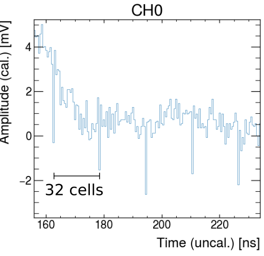
Thanks much for the quick reply. Ok, yes, things do seem ok after the offset calibration. I am running into some other issues I could use your advice on but will make a separate thread. As a preview, you can see hints in this waveform (periodic negative spikes).
This one should be considered resolved.
| Stefan Ritt wrote: |
|
Dear Sean,
noise in transparent mode comes from some coupling to your system clock. But 3.5 mV RMS seems rather hight to me. You should get it to below 1 mV if the DRS4 input is clean (try to short it).
The noise in the readout is expected. It looks exactly as Plot3 from the data sheet. You have to calibrate it away with a fixed offset for each cell as described in this paper: https://arxiv.org/abs/1405.4975 (paragraph IV. A. Voltage Calibration).
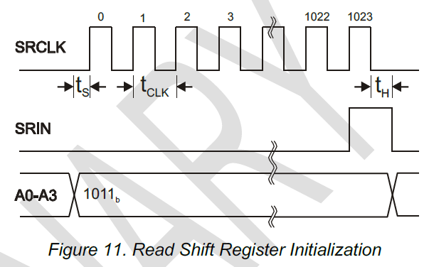
Concerning t_samp: Fig 11 in the datasheet just tells you that the rising edge of the SRCLK should come later than t_s after the address change. t_s is the setup time and 5 ns. Fig 12 tells you that the ADC should sample the analog output of the DRS t_samp after the address change A0-A3 and t_samp after the rising edge of SRCLK.
The digitizing speed of the evaluation board is indeed 15 MHz instead of the maximum 30 MHz, because this was easier to program in the FPGA. The t_samp has to be there so that the analog output signal of the DRS4 settles to its final value after each SRCLK pulse. If you sample "too early", you sample with the ADC the output when it is sill moving. So you have to wait until the analog is settled, but just before the next DRS sample becomes visible at the output. You can fine tune this with a differential probe at the DRS4 analog output (on a single ended probe you might drown in noise) on one channel of yoru scope and the ADC sample clock on the other channel of your scope. Note that the ADC sample clock cannot be derived straight from your FPGA clock, but you need some clock manager to fine-adjust its phase in 1ns steps.
But again, looking at your output, everything seems fine. You see the 5mV rms noise indicated in the datasheet table 1, which translates to about 20 mV peak-to-peak. If you do the offset calibration, this should go down to below 1 mV.
Best,
Stefan
| Sean Quinn wrote: |
|
Dear DRS4 team,
I'm experiencing some issues that seem to be isolated to the ASIC, and would like to understand if we are doing something wrong. There are several items to address in the post.
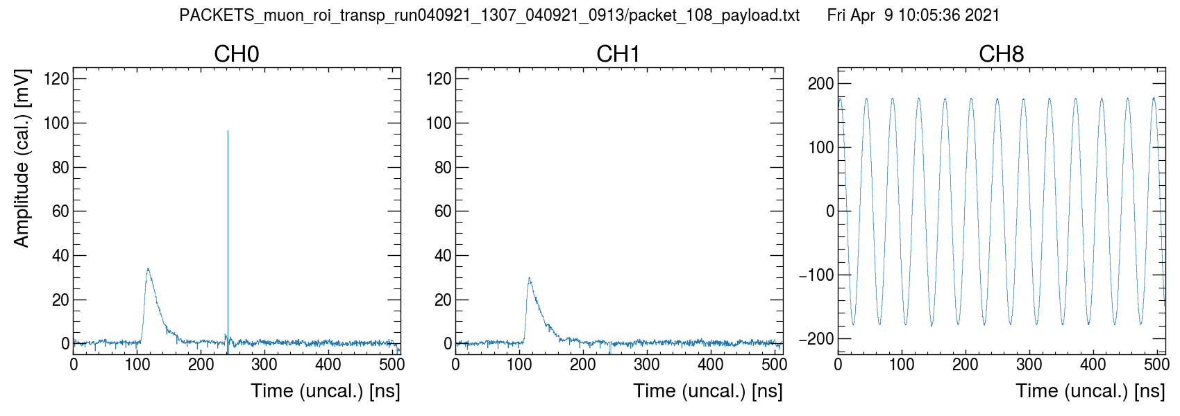
First, I do not think the noise observed is being injected from elsewhere on the board. If I run the DRS in transparent mode, the baseline noise is low, on order 3.5 mV (60 ADU), perhaps radiated from a clock. See below image. The scale is 0 to 1000 ADU with LSB = 6 uV (same AD9245 as eval board.). The DRS is in RUNNING state, I have forced a trigger in the ILA. This is for a single channel, CH0, 1024 cells.
In the next image, I show the waveform obtained from a full readout. This corresponds to ADC_READOUT state, and the plot uses the same 1000 ADU scale. Noise seems around 350 ADU now, many factors worse than before.
We've spent a lot of time trying to understand what's happening. One area that would be helpful to get some guidance on is the "t_samp" parameter. In Fig. 11 of the data sheet, should there be a t_samp label between t_s and t_clk? It just has arrows there with some width.
In our current firmware I believe R1 is simply one clock after R0 (for both ROI and full readout mode). Would this lead to the added noise observed in muxout?
This leads to the next question on what to actually use for t_samp. In the data sheet, page 4 "Timing Characteristics" it says to use t_samp = t0 + t_clk. Additionally, t0= 10 ns from that table. Fair enough.
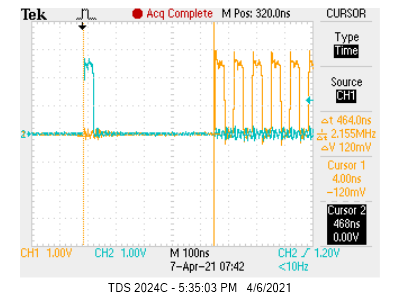
But if I check this against the eval board timing, I see very different values. Here the clock is 15 MHz so t_clk=67 ns (I note another post about this topic https://elog.psi.ch/elogs/DRS4+Forum/713), so I expect t_samp = 77 ns. But in practice it looks like the R0 to R1 delay is ~465 ns? (cyan=RSRLOAD, yellow=SRCLK)
Given this, is t_samp a value that should be tuned by the user?
Best regards,
Sean
|
|
|
|
|
823
|
Fri Apr 9 20:29:45 2021 |
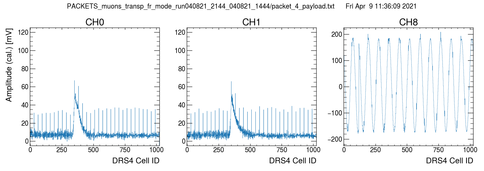
Sean Quinn | Spikes/noise sensitive to clock settings? | Dear DRS4 team,
I'm trying to troubleshoot some odd spike behavior. If I run the ADC and SR CLK at 16 MHz (behavior also seen at 33 MHz) we get very noisy data (post-calibration) with periodic spikes.
In the below plot
- CH0 & CH1 are muon pulses from a scintillator + SiPM detector
- CH8 is a 25 MHz sinewave (in phase with all generated board clocks)
- Transparent mode = ON
- ROI = OFF, "full readout mode", first sample = cell 0
- DRS REFCLK = 1 MHz (2 GS/s)
- ADC & SR CLK = 16 MHz, 0 deg. offset
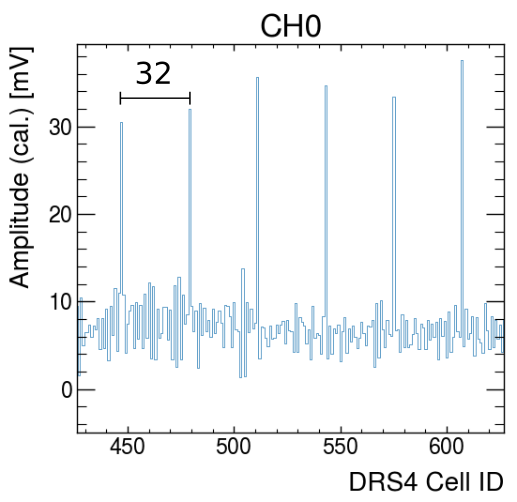
After I modify some clock settings, things seem to improve dramatically, and the spike behavior changes
- ADC and SR CLK = 15 MHz, 0 deg. offset
- Transparent mode = ON
- ROI = ON (just for testing purposes)
- Add 1.064 ns skew to DRS REF CLK
- NOTE: Unfortunately due to a design mishap, the ADC and FPGA clock use a phase-locked output pair on our clock synthesis chip, so we cannot fine-tune the skew for it.
Observed differences
- Spike polarity seems inverted
- Spikes limited to smaller number of cells now?
- Spike amplitude reduced
- Overall baseline variance seems better
- New large positive spike artifact on CH0 that seems inverted on CH1
- CH8 seems unaffected by large spikes?
Artifacts seem related to clock configuration, but I am sort of in the dark on what might be happening from a first-principles point of view. Any tips?
Warm regards,
Sean |
|
822
|
Fri Apr 9 20:22:13 2021 |
Sean Quinn | Unexpected noise in muxout: t_samp related? | Hi Stefan,
Thanks much for the quick reply. Ok, yes, things do seem ok after the offset calibration. I am running into some other issues I could use your advice on but will make a separate thread. As a preview, you can see hints in this waveform (periodic negative spikes).
This one should be considered resolved.
| Stefan Ritt wrote: |
|
Dear Sean,
noise in transparent mode comes from some coupling to your system clock. But 3.5 mV RMS seems rather hight to me. You should get it to below 1 mV if the DRS4 input is clean (try to short it).
The noise in the readout is expected. It looks exactly as Plot3 from the data sheet. You have to calibrate it away with a fixed offset for each cell as described in this paper: https://arxiv.org/abs/1405.4975 (paragraph IV. A. Voltage Calibration).
Concerning t_samp: Fig 11 in the datasheet just tells you that the rising edge of the SRCLK should come later than t_s after the address change. t_s is the setup time and 5 ns. Fig 12 tells you that the ADC should sample the analog output of the DRS t_samp after the address change A0-A3 and t_samp after the rising edge of SRCLK.
The digitizing speed of the evaluation board is indeed 15 MHz instead of the maximum 30 MHz, because this was easier to program in the FPGA. The t_samp has to be there so that the analog output signal of the DRS4 settles to its final value after each SRCLK pulse. If you sample "too early", you sample with the ADC the output when it is sill moving. So you have to wait until the analog is settled, but just before the next DRS sample becomes visible at the output. You can fine tune this with a differential probe at the DRS4 analog output (on a single ended probe you might drown in noise) on one channel of yoru scope and the ADC sample clock on the other channel of your scope. Note that the ADC sample clock cannot be derived straight from your FPGA clock, but you need some clock manager to fine-adjust its phase in 1ns steps.
But again, looking at your output, everything seems fine. You see the 5mV rms noise indicated in the datasheet table 1, which translates to about 20 mV peak-to-peak. If you do the offset calibration, this should go down to below 1 mV.
Best,
Stefan
| Sean Quinn wrote: |
|
Dear DRS4 team,
I'm experiencing some issues that seem to be isolated to the ASIC, and would like to understand if we are doing something wrong. There are several items to address in the post.
First, I do not think the noise observed is being injected from elsewhere on the board. If I run the DRS in transparent mode, the baseline noise is low, on order 3.5 mV (60 ADU), perhaps radiated from a clock. See below image. The scale is 0 to 1000 ADU with LSB = 6 uV (same AD9245 as eval board.). The DRS is in RUNNING state, I have forced a trigger in the ILA. This is for a single channel, CH0, 1024 cells.
In the next image, I show the waveform obtained from a full readout. This corresponds to ADC_READOUT state, and the plot uses the same 1000 ADU scale. Noise seems around 350 ADU now, many factors worse than before.
We've spent a lot of time trying to understand what's happening. One area that would be helpful to get some guidance on is the "t_samp" parameter. In Fig. 11 of the data sheet, should there be a t_samp label between t_s and t_clk? It just has arrows there with some width.
In our current firmware I believe R1 is simply one clock after R0 (for both ROI and full readout mode). Would this lead to the added noise observed in muxout?
This leads to the next question on what to actually use for t_samp. In the data sheet, page 4 "Timing Characteristics" it says to use t_samp = t0 + t_clk. Additionally, t0= 10 ns from that table. Fair enough.
But if I check this against the eval board timing, I see very different values. Here the clock is 15 MHz so t_clk=67 ns (I note another post about this topic https://elog.psi.ch/elogs/DRS4+Forum/713), so I expect t_samp = 77 ns. But in practice it looks like the R0 to R1 delay is ~465 ns? (cyan=RSRLOAD, yellow=SRCLK)
Given this, is t_samp a value that should be tuned by the user?
Best regards,
Sean
|
|
|
|
821
|
Wed Apr 7 08:26:12 2021 |
Stefan Ritt | Unexpected noise in muxout: t_samp related? | Dear Sean,
noise in transparent mode comes from some coupling to your system clock. But 3.5 mV RMS seems rather hight to me. You should get it to below 1 mV if the DRS4 input is clean (try to short it).
The noise in the readout is expected. It looks exactly as Plot3 from the data sheet. You have to calibrate it away with a fixed offset for each cell as described in this paper: https://arxiv.org/abs/1405.4975 (paragraph IV. A. Voltage Calibration).
Concerning t_samp: Fig 11 in the datasheet just tells you that the rising edge of the SRCLK should come later than t_s after the address change. t_s is the setup time and 5 ns. Fig 12 tells you that the ADC should sample the analog output of the DRS t_samp after the address change A0-A3 and t_samp after the rising edge of SRCLK.
The digitizing speed of the evaluation board is indeed 15 MHz instead of the maximum 30 MHz, because this was easier to program in the FPGA. The t_samp has to be there so that the analog output signal of the DRS4 settles to its final value after each SRCLK pulse. If you sample "too early", you sample with the ADC the output when it is sill moving. So you have to wait until the analog is settled, but just before the next DRS sample becomes visible at the output. You can fine tune this with a differential probe at the DRS4 analog output (on a single ended probe you might drown in noise) on one channel of yoru scope and the ADC sample clock on the other channel of your scope. Note that the ADC sample clock cannot be derived straight from your FPGA clock, but you need some clock manager to fine-adjust its phase in 1ns steps.
But again, looking at your output, everything seems fine. You see the 5mV rms noise indicated in the datasheet table 1, which translates to about 20 mV peak-to-peak. If you do the offset calibration, this should go down to below 1 mV.
Best,
Stefan
| Sean Quinn wrote: |
|
Dear DRS4 team,
I'm experiencing some issues that seem to be isolated to the ASIC, and would like to understand if we are doing something wrong. There are several items to address in the post.
First, I do not think the noise observed is being injected from elsewhere on the board. If I run the DRS in transparent mode, the baseline noise is low, on order 3.5 mV (60 ADU), perhaps radiated from a clock. See below image. The scale is 0 to 1000 ADU with LSB = 6 uV (same AD9245 as eval board.). The DRS is in RUNNING state, I have forced a trigger in the ILA. This is for a single channel, CH0, 1024 cells.
In the next image, I show the waveform obtained from a full readout. This corresponds to ADC_READOUT state, and the plot uses the same 1000 ADU scale. Noise seems around 350 ADU now, many factors worse than before.
We've spent a lot of time trying to understand what's happening. One area that would be helpful to get some guidance on is the "t_samp" parameter. In Fig. 11 of the data sheet, should there be a t_samp label between t_s and t_clk? It just has arrows there with some width.
In our current firmware I believe R1 is simply one clock after R0 (for both ROI and full readout mode). Would this lead to the added noise observed in muxout?
This leads to the next question on what to actually use for t_samp. In the data sheet, page 4 "Timing Characteristics" it says to use t_samp = t0 + t_clk. Additionally, t0= 10 ns from that table. Fair enough.
But if I check this against the eval board timing, I see very different values. Here the clock is 15 MHz so t_clk=67 ns (I note another post about this topic https://elog.psi.ch/elogs/DRS4+Forum/713), so I expect t_samp = 77 ns. But in practice it looks like the R0 to R1 delay is ~465 ns? (cyan=RSRLOAD, yellow=SRCLK)
Given this, is t_samp a value that should be tuned by the user?
Best regards,
Sean
|
|
|
820
|
Wed Apr 7 03:29:39 2021 |
Sean Quinn | Unexpected noise in muxout: t_samp related? | Dear DRS4 team,
I'm experiencing some issues that seem to be isolated to the ASIC, and would like to understand if we are doing something wrong. There are several items to address in the post.
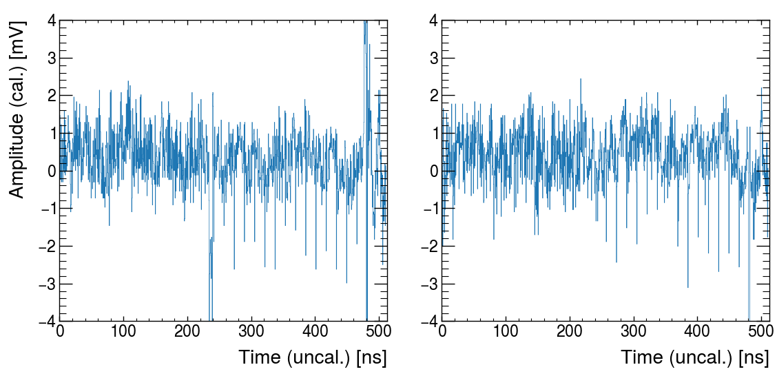
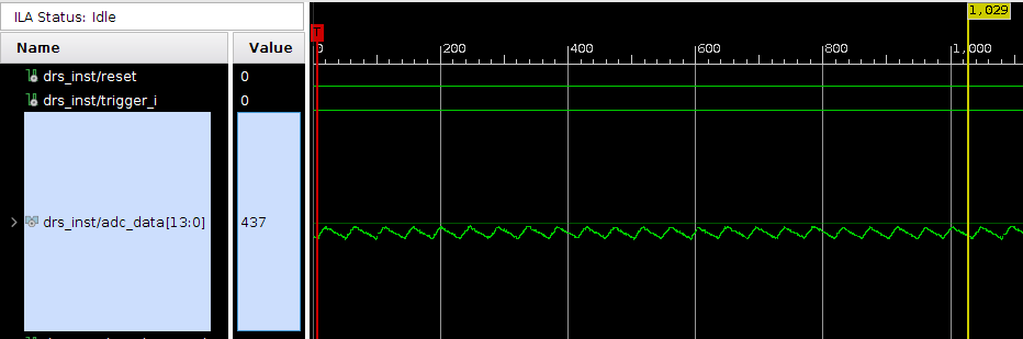
First, I do not think the noise observed is being injected from elsewhere on the board. If I run the DRS in transparent mode, the baseline noise is low, on order 3.5 mV (60 ADU), perhaps radiated from a clock. See below image. The scale is 0 to 1000 ADU with LSB = 6 uV (same AD9245 as eval board.). The DRS is in RUNNING state, I have forced a trigger in the ILA. This is for a single channel, CH0, 1024 cells.
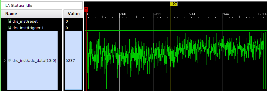
In the next image, I show the waveform obtained from a full readout. This corresponds to ADC_READOUT state, and the plot uses the same 1000 ADU scale. Noise seems around 350 ADU now, many factors worse than before.
We've spent a lot of time trying to understand what's happening. One area that would be helpful to get some guidance on is the "t_samp" parameter. In Fig. 11 of the data sheet, should there be a t_samp label between t_s and t_clk? It just has arrows there with some width.
In our current firmware I believe R1 is simply one clock after R0 (for both ROI and full readout mode). Would this lead to the added noise observed in muxout?
This leads to the next question on what to actually use for t_samp. In the data sheet, page 4 "Timing Characteristics" it says to use t_samp = t0 + t_clk. Additionally, t0= 10 ns from that table. Fair enough.
But if I check this against the eval board timing, I see very different values. Here the clock is 15 MHz so t_clk=67 ns (I note another post about this topic https://elog.psi.ch/elogs/DRS4+Forum/713), so I expect t_samp = 77 ns. But in practice it looks like the R0 to R1 delay is ~465 ns? (cyan=RSRLOAD, yellow=SRCLK)
Given this, is t_samp a value that should be tuned by the user?
Best regards,
Sean
|
|
819
|
Fri Mar 5 09:39:42 2021 |
Stefan Ritt | Trouble getting PLL to lock | That probably depends on the way your FPGA boots. If the SRCLK signal goes high after the SRIN - even a few ns - you might clock one or two zeros into the config register, thus disabling the PLL. Shame that I haven't thought of this before.
Stefan |
|
818
|
Thu Mar 4 21:36:14 2021 |
Tom Schneider | Trouble getting PLL to lock | I found the problem, and it had nothing to do with the CMOS clock input. As it turns out, even though I was using the default state of the config register, I still had to write to it after powerup. Once I did that, the PLL locked immediately.
-Tom
| Tom Schneider wrote: |
|
Thats not a simple modification to my PCB, but I'll give it a try. Thanks for your help
| Stefan Ritt wrote: |
|
Sounds to me like your REFCLK is not getting through or your PLL loop is open. Could be a bad solder connection. Try to measure signals not on the PCB trace, but directly on the DRS4 pins. Drive REFCLK with a proper LVDS signal. Maybe it's wrong what I wrote in the data sheet and the trick with VDD/2 is not really working.
Stefan
|
|
|
|
817
|
Fri Feb 26 22:52:13 2021 |
Tom Schneider | Trouble getting PLL to lock | Thats not a simple modification to my PCB, but I'll give it a try. Thanks for your help
| Stefan Ritt wrote: |
|
Sounds to me like your REFCLK is not getting through or your PLL loop is open. Could be a bad solder connection. Try to measure signals not on the PCB trace, but directly on the DRS4 pins. Drive REFCLK with a proper LVDS signal. Maybe it's wrong what I wrote in the data sheet and the trick with VDD/2 is not really working.
Stefan
|
|
|
816
|
Fri Feb 26 22:12:58 2021 |
Stefan Ritt | Trouble getting PLL to lock | Sounds to me like your REFCLK is not getting through or your PLL loop is open. Could be a bad solder connection. Try to measure signals not on the PCB trace, but directly on the DRS4 pins. Drive REFCLK with a proper LVDS signal. Maybe it's wrong what I wrote in the data sheet and the trick with VDD/2 is not really working.
Stefan |
|
815
|
Fri Feb 26 21:24:39 2021 |
Tom Schneider | Trouble getting PLL to lock | Probe capacitance makes that tricky - if I put my probe on DSPEED, I see that it starts at approx. 2.5V then gradually decreases until it hits 0V. DTAP decreases from 3MHz to 0 during this time.
I'll try to get something together to show you.
| Stefan Ritt wrote: |
|
Can you post a scope trace of your refclk together with DTAP, DSPEED and DENABLE?
| Tom Schneider wrote: |
|
Stefan,
Thanks for responding so quickly. Yes I have my clock source going to REFCLK+ (CLKIN is the signal name on my schematic). BIAS is 0.7V exactly, /RESET is high, A0-A3 are 0x0000, and the loop filter has a 4.7nF cap to GND with a 130ohm resistor + 1uF cap in parallel, just like the eval board.
Regarding the clock - I am not using an LVDS clock, but rather a 2.5V-level clock signal, with REFCLK- tied to 1.25V. Sheet 9 of the datasheet states: If no LVDS reference clock signal is available, a CMOS signal can be connected to REFCLK+ and the REFCLK input is connected to VDD/2 via a resistor divider.
Is that not a true statement?
-Tom
| Stefan Ritt wrote: |
|
I guess you mean "1 MHz clock at REFCLK+", and not CLKIN, there is no CLKIN, just a SRCLK, but that is someting else!
There could be many reasons why this is not working. It's hard for me to debug your board without actually having it in hands. So just some ideas:
- Supply a clean differential REFCLK, I never tried one end tied to VDD/2
- Is /RESET high?
- Is BIAS at roughly 0.7V?
- Is A0-A3 different from 1111, which puts the chip in standby
- Did you double check your loop filter?
The easiest usually is to start from a running evaluation board, then compare all pins 1:1 with your board.
Stefan
| Tom Schneider wrote: |
|
Hello,
I am working on a custom PCB design with the DRS4 chip, and I can't get the PLL to lock. I'm feeding CLKIN with a 1MHz CMOS clock (REFCLK- tied to VDD/2), and I'm using the same loop filter as the eval board. I see from the datasheet that the PLL is enabled by default, so I'm not writing anything to the config register on startup. I am just driving DENABLE high approx. 100ms after startup and looking for the PLL lock bit to go high. When I look at DTAP, I see a 3MHz signal. Can anyone tell me what I'm doing wrong?
-Tom
|
|
|
|
|
|
814
|
Fri Feb 26 20:32:25 2021 |
Stefan Ritt | Trouble getting PLL to lock | Can you post a scope trace of your refclk together with DTAP, DSPEED and DENABLE?
| Tom Schneider wrote: |
|
Stefan,
Thanks for responding so quickly. Yes I have my clock source going to REFCLK+ (CLKIN is the signal name on my schematic). BIAS is 0.7V exactly, /RESET is high, A0-A3 are 0x0000, and the loop filter has a 4.7nF cap to GND with a 130ohm resistor + 1uF cap in parallel, just like the eval board.
Regarding the clock - I am not using an LVDS clock, but rather a 2.5V-level clock signal, with REFCLK- tied to 1.25V. Sheet 9 of the datasheet states: If no LVDS reference clock signal is available, a CMOS signal can be connected to REFCLK+ and the REFCLK input is connected to VDD/2 via a resistor divider.
Is that not a true statement?
-Tom
| Stefan Ritt wrote: |
|
I guess you mean "1 MHz clock at REFCLK+", and not CLKIN, there is no CLKIN, just a SRCLK, but that is someting else!
There could be many reasons why this is not working. It's hard for me to debug your board without actually having it in hands. So just some ideas:
- Supply a clean differential REFCLK, I never tried one end tied to VDD/2
- Is /RESET high?
- Is BIAS at roughly 0.7V?
- Is A0-A3 different from 1111, which puts the chip in standby
- Did you double check your loop filter?
The easiest usually is to start from a running evaluation board, then compare all pins 1:1 with your board.
Stefan
| Tom Schneider wrote: |
|
Hello,
I am working on a custom PCB design with the DRS4 chip, and I can't get the PLL to lock. I'm feeding CLKIN with a 1MHz CMOS clock (REFCLK- tied to VDD/2), and I'm using the same loop filter as the eval board. I see from the datasheet that the PLL is enabled by default, so I'm not writing anything to the config register on startup. I am just driving DENABLE high approx. 100ms after startup and looking for the PLL lock bit to go high. When I look at DTAP, I see a 3MHz signal. Can anyone tell me what I'm doing wrong?
-Tom
|
|
|
|
|
813
|
Fri Feb 26 18:33:52 2021 |
Tom Schneider | Trouble getting PLL to lock | Stefan,
Thanks for responding so quickly. Yes I have my clock source going to REFCLK+ (CLKIN is the signal name on my schematic). BIAS is 0.7V exactly, /RESET is high, A0-A3 are 0x0000, and the loop filter has a 4.7nF cap to GND with a 130ohm resistor + 1uF cap in parallel, just like the eval board.
Regarding the clock - I am not using an LVDS clock, but rather a 2.5V-level clock signal, with REFCLK- tied to 1.25V. Sheet 9 of the datasheet states: If no LVDS reference clock signal is available, a CMOS signal can be connected to REFCLK+ and the REFCLK input is connected to VDD/2 via a resistor divider.
Is that not a true statement?
-Tom
| Stefan Ritt wrote: |
|
I guess you mean "1 MHz clock at REFCLK+", and not CLKIN, there is no CLKIN, just a SRCLK, but that is someting else!
There could be many reasons why this is not working. It's hard for me to debug your board without actually having it in hands. So just some ideas:
- Supply a clean differential REFCLK, I never tried one end tied to VDD/2
- Is /RESET high?
- Is BIAS at roughly 0.7V?
- Is A0-A3 different from 1111, which puts the chip in standby
- Did you double check your loop filter?
The easiest usually is to start from a running evaluation board, then compare all pins 1:1 with your board.
Stefan
| Tom Schneider wrote: |
|
Hello,
I am working on a custom PCB design with the DRS4 chip, and I can't get the PLL to lock. I'm feeding CLKIN with a 1MHz CMOS clock (REFCLK- tied to VDD/2), and I'm using the same loop filter as the eval board. I see from the datasheet that the PLL is enabled by default, so I'm not writing anything to the config register on startup. I am just driving DENABLE high approx. 100ms after startup and looking for the PLL lock bit to go high. When I look at DTAP, I see a 3MHz signal. Can anyone tell me what I'm doing wrong?
-Tom
|
|
|
|
812
|
Fri Feb 26 17:59:14 2021 |
Stefan Ritt | Trouble getting PLL to lock | I guess you mean "1 MHz clock at REFCLK+", and not CLKIN, there is no CLKIN, just a SRCLK, but that is someting else!
There could be many reasons why this is not working. It's hard for me to debug your board without actually having it in hands. So just some ideas:
- Supply a clean differential REFCLK, I never tried one end tied to VDD/2
- Is /RESET high?
- Is BIAS at roughly 0.7V?
- Is A0-A3 different from 1111, which puts the chip in standby
- Did you double check your loop filter?
The easiest usually is to start from a running evaluation board, then compare all pins 1:1 with your board.
Stefan
| Tom Schneider wrote: |
|
Hello,
I am working on a custom PCB design with the DRS4 chip, and I can't get the PLL to lock. I'm feeding CLKIN with a 1MHz CMOS clock (REFCLK- tied to VDD/2), and I'm using the same loop filter as the eval board. I see from the datasheet that the PLL is enabled by default, so I'm not writing anything to the config register on startup. I am just driving DENABLE high approx. 100ms after startup and looking for the PLL lock bit to go high. When I look at DTAP, I see a 3MHz signal. Can anyone tell me what I'm doing wrong?
-Tom
|
|
|
811
|
Fri Feb 26 17:05:26 2021 |
Tom Schneider | Trouble getting PLL to lock | Hello,
I am working on a custom PCB design with the DRS4 chip, and I can't get the PLL to lock. I'm feeding CLKIN with a 1MHz CMOS clock (REFCLK- tied to VDD/2), and I'm using the same loop filter as the eval board. I see from the datasheet that the PLL is enabled by default, so I'm not writing anything to the config register on startup. I am just driving DENABLE high approx. 100ms after startup and looking for the PLL lock bit to go high. When I look at DTAP, I see a 3MHz signal. Can anyone tell me what I'm doing wrong?
-Tom |
|
810
|
Fri Feb 26 08:52:50 2021 |
Stefan Ritt | DRS spike removal for multiple waveforms | Just look at the definition of the function below, all parameters are explained there. In meantime we have a firmware fix to avoid the spikes inside the chip, but I have not yet found time to update the evaluation board.
Stefan
void DRSBoard::RemoveSymmetricSpikes(short **wf, int nwf,
short diffThreshold, int spikeWidth,
short maxPeakToPeak, short spikeVoltage,
int nTimeRegionThreshold)
{
// Remove a specific kind of spike on DRS4.
// This spike has some features,
// - Common on all the channels on a chip
// - Constant heigh and width
// - Two spikes per channel
// - Symmetric to cell #0.
//
// This is not general purpose spike-removing function.
//
// wf : Waveform data. cell#0 must be at bin0,
// and number of bins must be kNumberOfBins.
// nwf : Number of channels which "wf" holds.
// diffThreshold : Amplitude threshold to find peak
// spikeWidth : Width of spike
// maxPeakToPeak : When peak-to-peak is larger than this, the channel
// is not used to find spikes.
// spikeVoltage : Amplitude of spikes. When it is 0, it is calculated in this function
// from voltage difference from neighboring bins.
// nTimeRegionThreshold : Requirement of number of time regions having spike at common position.
// Total number of time regions is 2*"nwf". |
|
809
|
Thu Feb 25 17:56:39 2021 |
Matthias Plum | DRS spike removal for multiple waveforms | Hi,
Is there a way that someone can help me and my student to enable RemoveSymmetricSpikes function in the drs_exam.cpp? We are not 100% sure how to call the function if you want to read out four waveforms.
Cheers,
Matthias |
|
808
|
Wed Jan 20 17:37:51 2021 |
Stefan Ritt | drs4 persistence | The chip itself can only sample a single waveform, that must be done in the attached software. The current DRSOscilloscope software coming with the evaluation board has not yet implemented that, but if you write your own software you can do so.
| Taegyu Lee wrote: |
|
Dear all,
I have a question about the function that drs4 can perform.
Is there any function in drs4 that is analogous to that of "persistence display" in oscilloscope?? (accumulating pulses)
Thank you
|
|
|
807
|
Wed Jan 20 12:14:49 2021 |
Taegyu Lee | drs4 persistence | Dear all,
I have a question about the function that drs4 can perform.
Is there any function in drs4 that is analogous to that of "persistence display" in oscilloscope?? (accumulating pulses)
Thank you |
|
806
|
Thu Dec 17 11:31:34 2020 |
Stefan Ritt | drs sources on github? | Not github, but bitbucket: https://bitbucket.org/ritt/drs4eb/src/master/
But development kind of stalled, so there will be updates only in case of severe bugs, which are kind of gone after 10 years now.
Best,
Stefan
> Are there plans to add the drs software to github? (asking because I have users @ethz.ch that want to use it on debian,
> thus I'm creating official debian packages of it, if license allows so, but talking to upstream (the developers) would be
> much easier on github (or irc) than on this "DRS4 Discussion Forum".
>
> Best, |
|