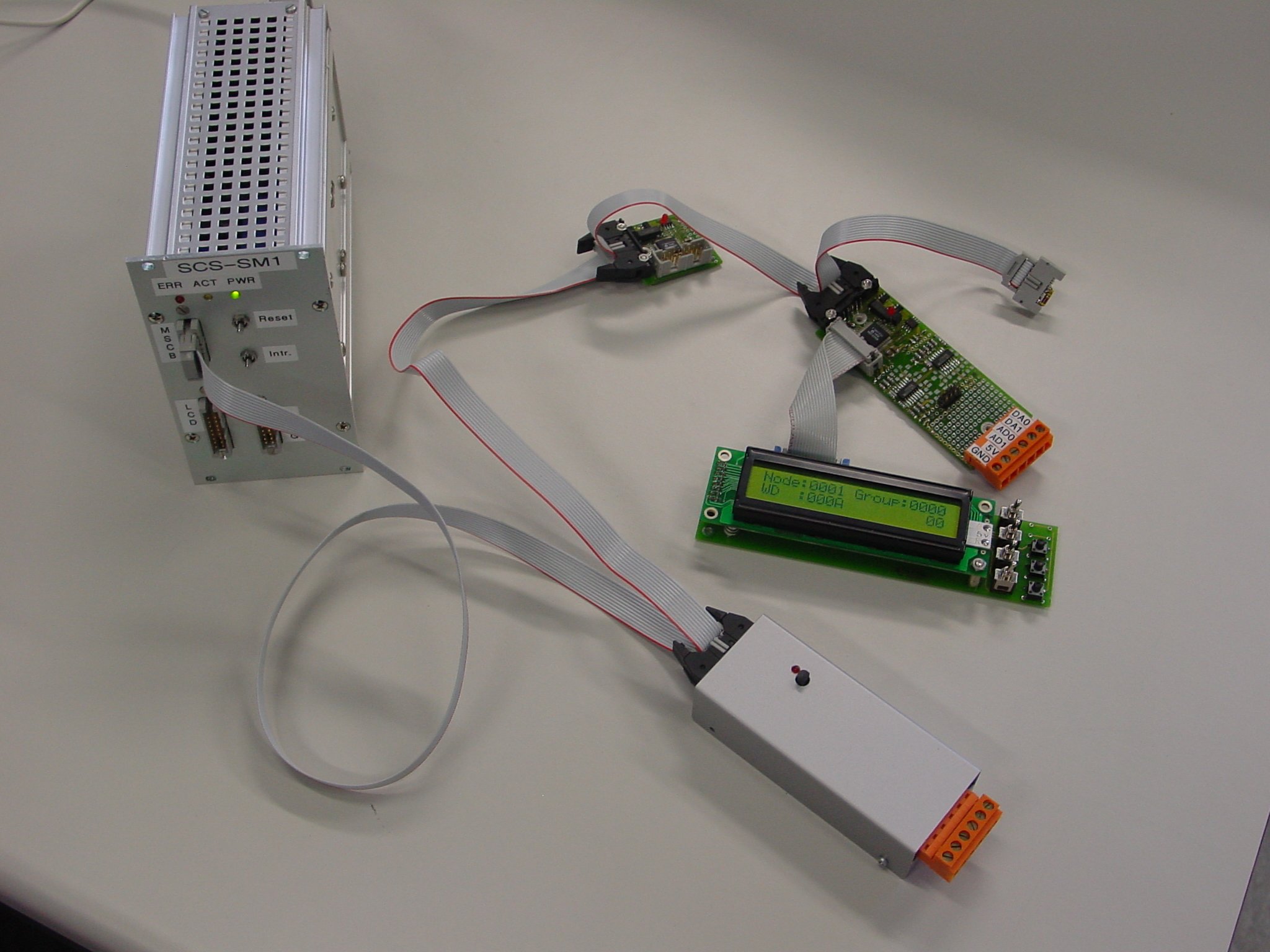
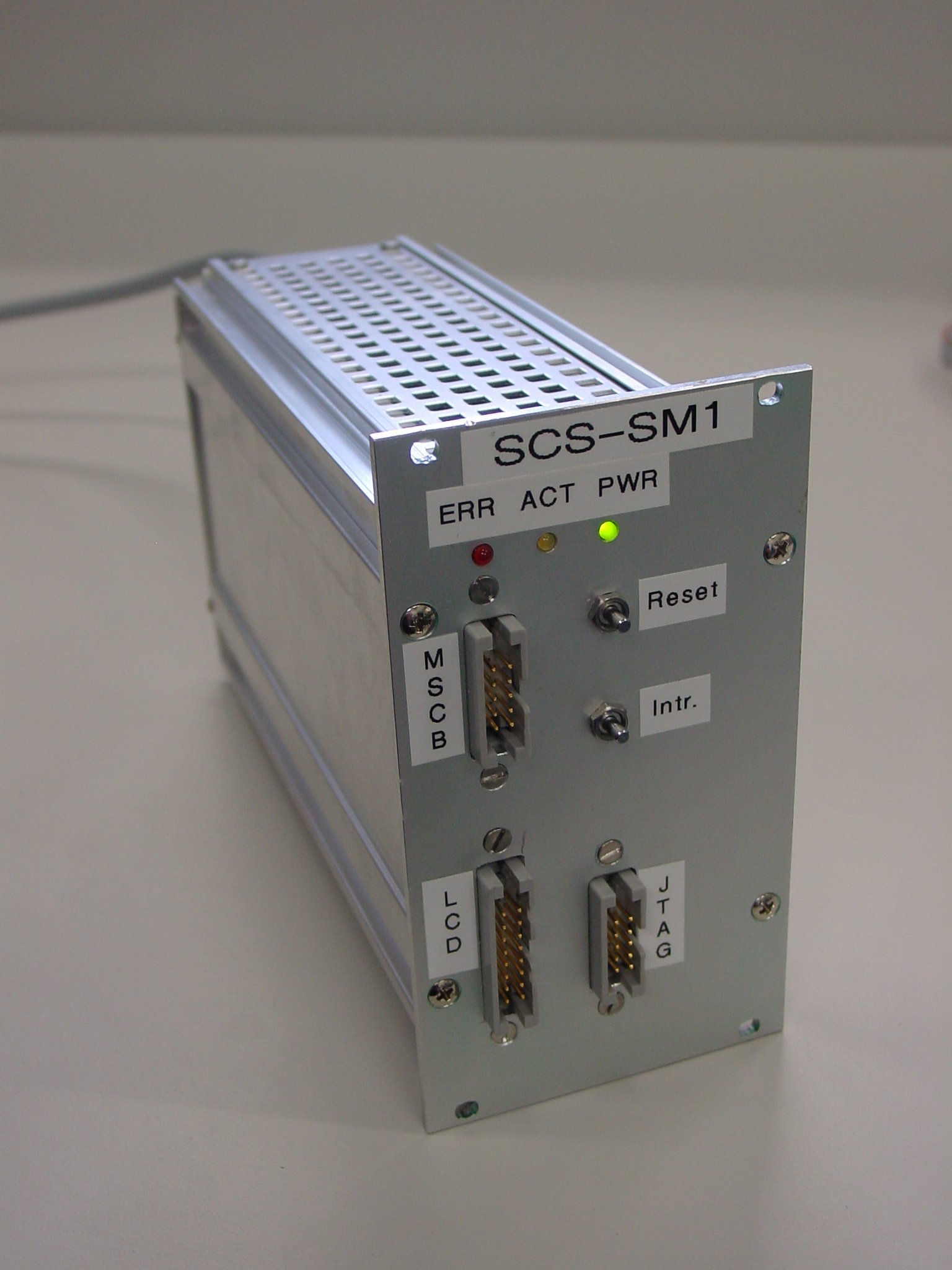
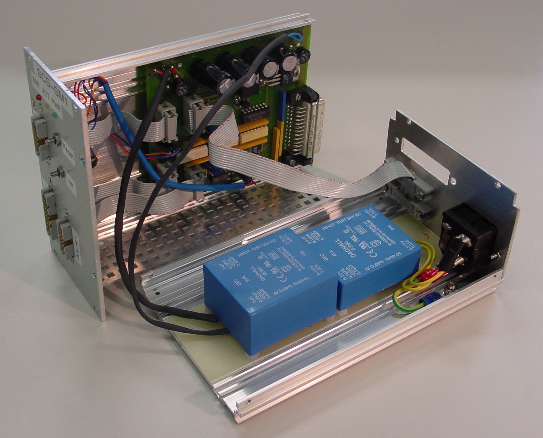
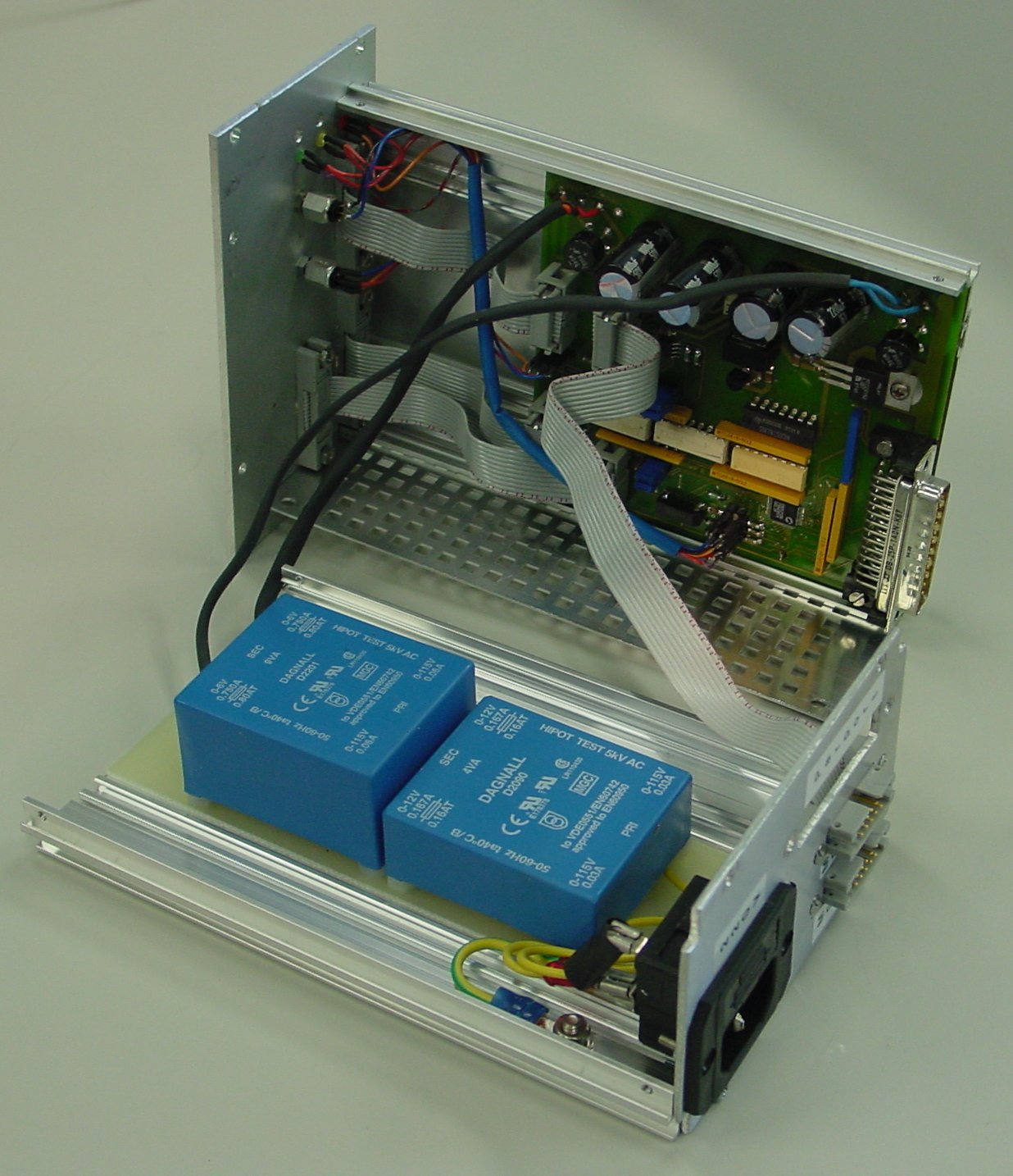
Submaster SCS-SM1
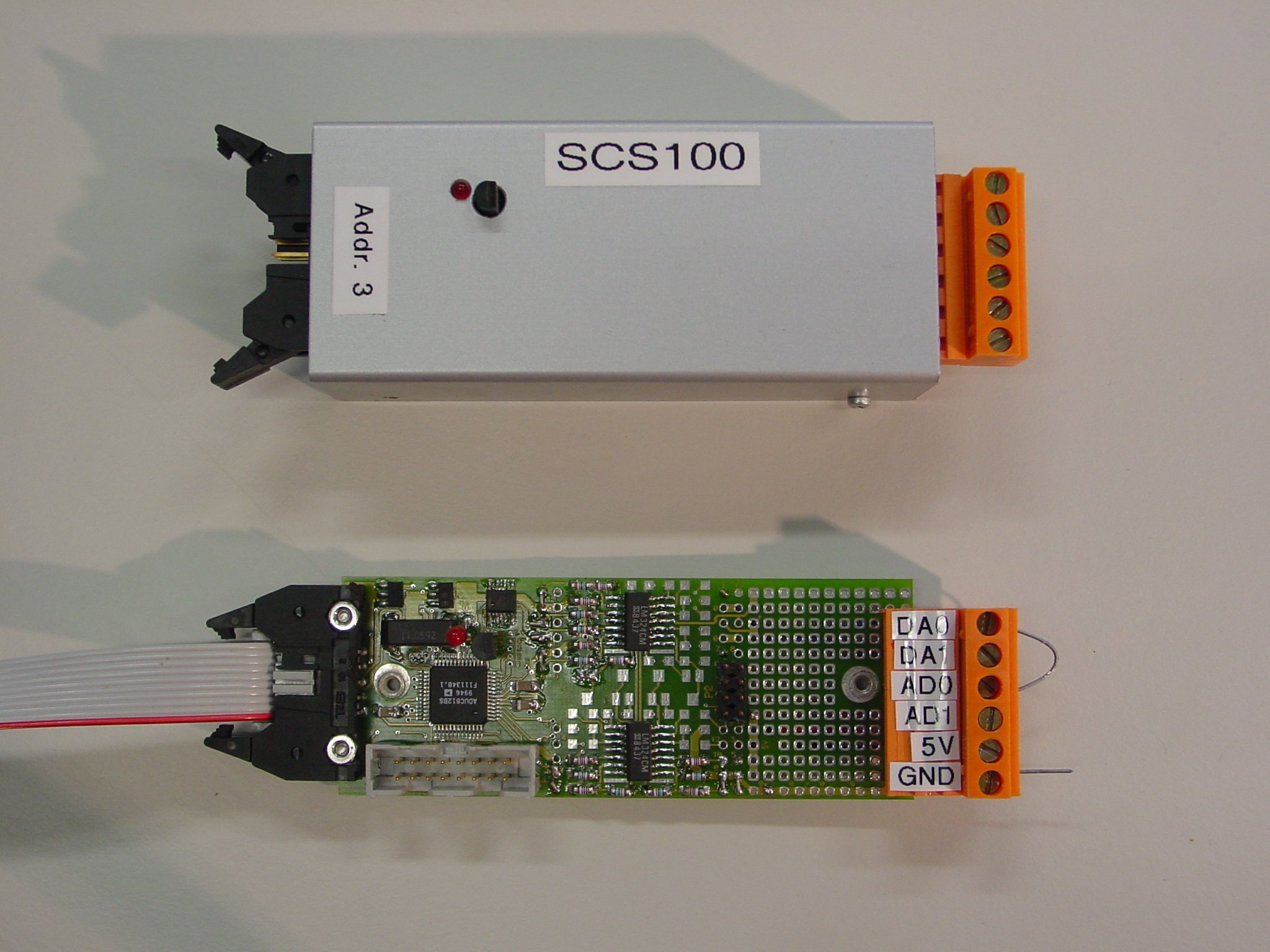
General purpose node SCS100
Mini piggy-back node SCS101
LCD module SCS-LCD1
High voltage node SCS-HV1
Planned modules
Back
|
RS-485 Bus Submaster SCS-SM1 General purpose node SCS100 Mini piggy-back node SCS101 LCD module SCS-LCD1 High voltage node SCS-HV1 Planned modules Back |
|
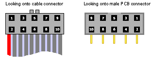
| Pin1 | Pin2 | Pin3 | Pin4 | Pin5 | Pin6 | Pin7 | Pin8 | Pin9 | Pin10 |
|---|---|---|---|---|---|---|---|---|---|
| Data A | Data B | -15V | +15V | +5V | GND | Reset | Interrupt | reserved | reserved |
 | |||||||||
The RS-485 bus is used in many industrial applications and other field buses. Some nice introduction can be found here and here.
Due to the differential signalling, it is relatively immune to noise when using twisted pair cables. Depending on the speed, the bus can easily be run at distances from 100m to a few km. If the bus becomes long (> serveral hundred meters), a bus termination is required which matches the impedance of the twisted pair cable. The bus runs at a speed of 345600 Baud but can be slowed down if necessary. Unlike the RS-232 standard, the RS-485 is a multi-drop half-duplex bus, which means that many nodes can be connected to the same bus, but only one node at a time can send data. The RS-485 tranceivers in the SCS100 and SCS101 nodes present "1/8 load" to the bus, which means that 256 nodes can be directly connected to the same bus segment. If more nodes are needed, repeaters have to be used.
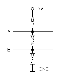
It should be noted that the MSCB bus only needs the A,B and GND wires to function, if the node power is supplied locally, and the interrupt and reset functionality is not necessary. In this case, simple two wire shielded twisted pair cable can be used. It is then recommended to use opto-couplers after the RS-485 transceivers to avoid ground loops.
In order to set the A and B line to a defined level in case no node is active, two pull up / pull down resistors are required. These resistors, together with a 100 Ohm termination resistor, are per definition implemented at that point where the power is applied to the bus, to avoid double termination as shown in the following figure:
When looking at the RS-485 line "A" (pin 1) with a scope, following bit pattern can be seen:
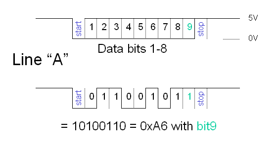
After a negative start bit, we have 8 data bits with the LSB first, positive logic. The bit 9 is set only in addressing commands, followed by a positive stop bit. Line "B" is inverted.
In addition the SM1 module contains a power supply which can be used to power 10-20 nodes on the bus. Three unregulated voltages of +6V, +15V and -15V are supplied, so that small 78L05 type regulators can be used on the nodes to produce a clean +5V power supply.
A front panel button can be used to distribute an interrupt signal to all nodes on the bus, which can be used for example to switch of high voltages in an emergency case. Since this button is directly connected to a dedicated bus line, it works even if the microcontroller of the SM1 is malfunctioning.
|
Power: 220V or 110V Connection to PC: Standard Sub-D 25 connector Internal microcontroller: Cygnal C8051F236 running at 11.0592MHz Power supply to bus: +6V, 1.5A, unregulated; +15V, -15V, 0.2A, unregulated Bus connection: decoupled via optocouplers Front panel elements: 3 LED (power, activity, error), reset and interrupt button MSCB bus connectors: 1 (front side) plus 2 (back side) Other connectors: JTAG for programming the Cygnal microcontroller and interface to SCS-LCD1 module (very roughly) estimated price of parts: 50US$ Schematics, as PDF file, Layout |
|  |
|
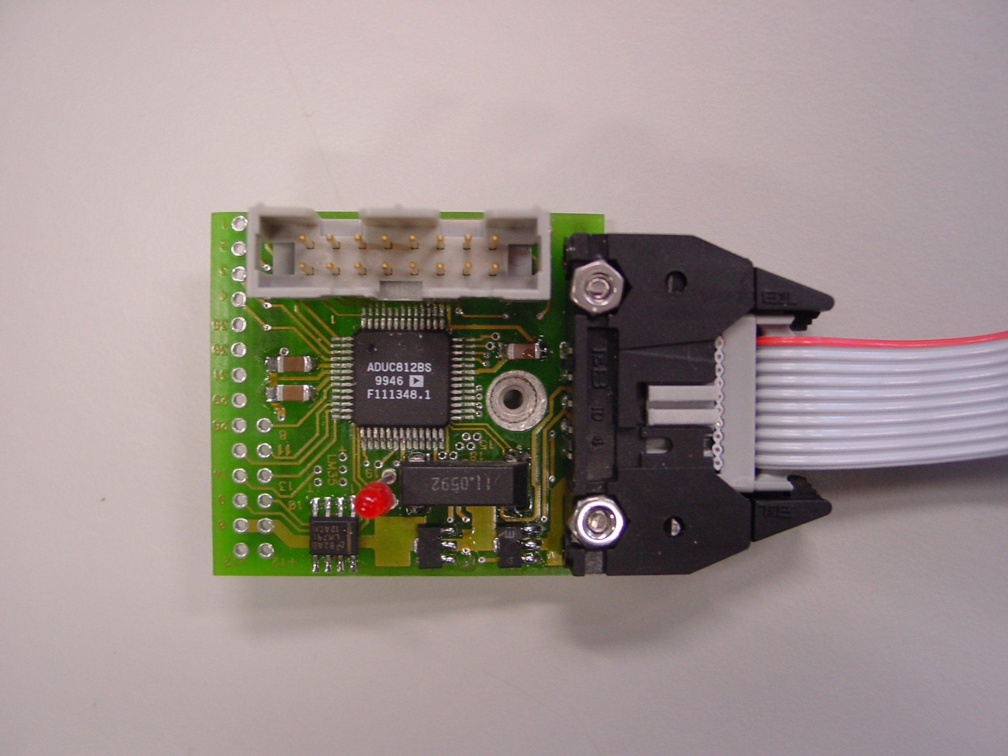
Size (without connector): (LWH) 96mm x 32mm x 13mm Power supply: received from bus, regulated to +5V, +12V and -12V Microcontroller: Analog Devices ADuC812 running at 11.0592MHz LED: On when node is addressed Temperature sensors: LM35, thermocouple inside the ADuC812 Connectors: 10-pin MSCB and 16-pin interface to SCS-LCD1 module and for ADuC812 programming Ports: 8-bit TTL I/O (P2 of microcontroller), 8 channels ADC 12 bit, 200kHz, 2 channels DAC 12 bit OpAmps: two quad op-amps (LM324 or OP400 for higher precision with offset and drifts in the microvolt region) Prototype area:25mm x 30mm Price of parts and assembly: ~25US$ Schematics, as PDF file, Layout |
|
Size (without connector): (LWH) 40mm x 32mm x 13mm Power supply: received from bus, regulated to +5V, +12V and -12V Microcontroller: Analog Devices ADuC812 running at 11.0592MHz LED: On when node is addressed Temperature sensors: LM35, thermocouple inside the ADuC812 Connectors: 10-pin MSCB and 16-pin interface to SCS-LCD1 module and for ADuC812 programming Ports: 5-bit TTL I/O (partial P2 of microcontroller), 8 channels ADC 12 bit, 200kHz, 2 channels DAC 12 bit Price of parts and assembly: ~23US$ Schematics (same as SCS100, second page), as PDF file, Layout |

|
Size (without connector): (LWH) 145mm x 38mm x 23mm Power supply: +5V received from connector LCD display: Anag Vision AV2020, 20x2 character, backlight or similar display with HD44780/KS0066 controller Switches: 4, accessible by SCS100/SCS101/SCS-SM1 microcontroller Button: 4, accessible by SCS100/SCS101/SCS-SM1 microcontroller Price of parts and assembly: ~40 US$ Schematics, as PDF file |
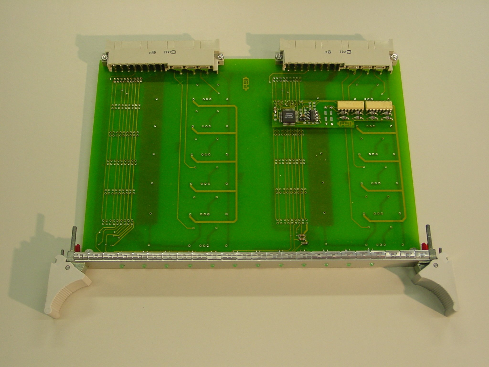
A motherboard houses 12 channels and a 19" crate houses 16 boards, which makes 192 channels for a 19" crate. Each channel is connected to a LED on the fron panel for status display and to a HV connector at the back plane.
To compensate for temperature drifts in the DAC/ADC, a global high accuracy reference voltage is distributed through the crate, which is measured at every node. This allows a software correction for various drifts. In addition to that, the integrated temperature sensor of the microcontroller is used to compensate temperature drifts of some resistors.
The development of this system is still in progress so the quoted numbers are preliminary.
|
Size: 6U height motherboard housing 12 channels Power supply: +5V, -5V from backplane and global HV 0..2400V Accuracy (target value): +-0.3V at 1000V between 20deg.C and 40deg.C absolute, reproducibility and stability <0.1V Price per channel of a full crate: 35 US$ Positive HV: Schematics, as PDF file, Layout Negative HV: Schematics, as PDF file, Layout |