|
The design of high frequency differential input stages with the DRS4 is a challenge, since the chip draws quite some current at the input (up to 1 mA at 5 GSPS), which must be sourced by the input buffer. A simple transformer as used in the DRS4 Evaluation Board 2.0 limits the bandwidth to 220 MHz. In meantime two active input stages have been worked out and successfully been tested, both utilizing the THS4508 differential amplifier. The first design is AC-coupled and uses less power, the second design is DC-coupled and uses more power with the benefit of delivering a higher bandwidth.
Both designs use a clamping diode at the input as a protection against high voltage spikes at the input. We used a RCLAMP0502B diode from SEMTECH, but any fast voltage suppressor diode will do the job.
The CMOFS input to the THS4508 set the common mode of the differential amplifier. In the AC version the level is set to mid-rail (2.5V), in the DC version it's set to 1.8V to match the input range of the DRS4.
The CAL+ and CAL- signals are used to bias the inputs to a well-defined DC level and can also be used to calibrate the chip. For bipolar inputs, they are both set to 0.8V. A positive 0.5V input pulse then drives DRS_IN+ to (0.8+0.25)V = 1.05V and DRS_IN- to (0.8-0.25)V = 0.55V. A negative 0.5V pulse then drives then DRS_IN+ to 0.55V and DRS_IN- to 1.05V. With ROFS=1.6V, the full dynamic range of the DRS4 is then used. Note that the THS4508 has a gain of 2, and the input has a -6dB voltage divider to compensate for that. To use other input ranges, such as -1V...0V, the CAL+ and CAL- signals can be adjusted accordingly. Note that the inputs of the DRS4 must always be between 0.1V and 1.5V.
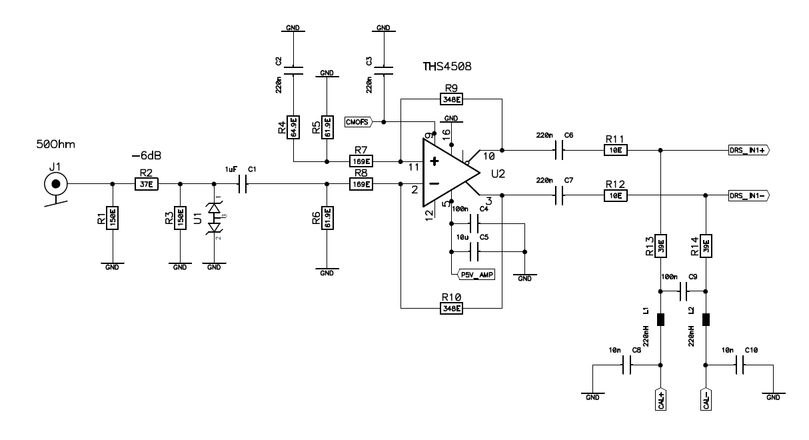
AC-coupled version
(click to enlarge)
Power supply: +5 V 40 mA
Bandwidth (-3dB): 600 MHz
CMOFS: 2.5 V
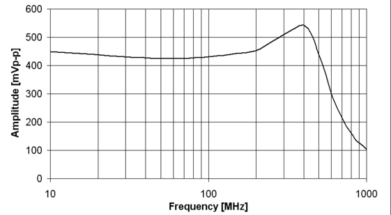
Transfer function:
(click to enlarge)
The transfer function was measured by applying a fixed amplitude sine wave to the input, and measuring the peak-to-peak value of the read out waveform with the DRSOsc application.
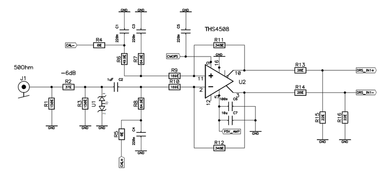
DC-coupled Version
The DC-coupled version has a slightly higher power consumption since there is a constant current flowing through the output into the DRS4 chip. On the other hand, the bandwidth is a bit higher and the peaking around 400 MHz is a bit smaller. The input is still AC-coupled, so both positive and negative pulses can be accepted.
(click to enlarge)
Power supply: +5 V 115 mA
Bandwidth (-3dB): 800 MHz
CMOFS: 1.8 V
Transfer function:
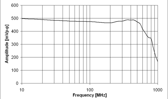
(click to enlarge)
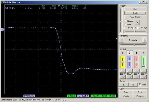
Achievable performance
With the active input stage, much faster rise- and fall times can be achieved. Following picture shows a signal from a external clock having a fall time of about 300 ps being recorded with the AC-coupled version of the active input stage. The fall time of the recorded signal is about 800 ps, which is about the minimum which can be achieved with the AC-coupled version. The DC-coupled version achieves about 700ps.
|