DRS4 Forum
  DRS4 Discussion Forum  Not logged in ELOG logo
Entry  Wed Apr 7 03:29:39 2021, Sean Quinn, Unexpected noise in muxout: t_samp related? transp_example.PNGtransp_readout_example_noise.PNGdrs_datasheet_fig11.PNGr0_r1_delay.png
    Reply  Wed Apr 7 08:26:12 2021, Stefan Ritt, Unexpected noise in muxout: t_samp related? 
       Reply  Fri Apr 9 20:22:13 2021, Sean Quinn, Unexpected noise in muxout: t_samp related? ex_cal_wave.png
          Reply  Fri Apr 9 20:55:28 2021, Stefan Ritt, Unexpected noise in muxout: t_samp related? 
             Reply  Fri Apr 9 21:56:54 2021, Sean Quinn, Unexpected noise in muxout: t_samp related? 
Message ID: 826     Entry time: Fri Apr 9 21:56:54 2021     In reply to: 824
Author: Sean Quinn 
Subject: Unexpected noise in muxout: t_samp related? 

Yes, there is some systematic board noise on this prototype, unfortunately sad

Ok, then it seems the other post I made might still belong in this thread after all.

Thanks for confirming negative spike behavior, we now have a mitigation plan going forward.


Cheers,

Stefan Ritt wrote:

If you do the cell calibration correctly, your noise should be ~0.4 mV. You seem to be 2-3x larger. The periodic negative spikes come if you dont' sample at the right time. Adjust t_samp until they are gone.

Stefan

Sean Quinn wrote:

Hi Stefan,


Thanks much for the quick reply. Ok, yes, things do seem ok after the offset calibration. I am running into some other issues I could use your advice on but will make a separate thread. As a preview, you can see hints in this waveform (periodic negative spikes).

 This one should be considered resolved.

Stefan Ritt wrote:

Dear Sean,

noise in transparent mode comes from some coupling to your system clock. But 3.5 mV RMS seems rather hight to me. You should get it to below 1 mV if the DRS4 input is clean (try to short it).

The noise in the readout is expected. It looks exactly as Plot3 from the data sheet. You have to calibrate it away with a fixed offset for each cell as described in this paper: https://arxiv.org/abs/1405.4975 (paragraph IV. A. Voltage Calibration).

Concerning t_samp: Fig 11 in the datasheet just tells you that the rising edge of the SRCLK should come later than t_s after the address change. t_s is the setup time and 5 ns. Fig 12 tells you that the ADC should sample the analog output of the DRS t_samp after the address change A0-A3 and t_samp after the rising edge of SRCLK. 

The digitizing speed of the evaluation board is indeed 15 MHz instead of the maximum 30 MHz, because this was easier to program in the FPGA. The t_samp has to be there so that the analog output signal of the DRS4 settles to its final value after each SRCLK pulse. If you sample "too early", you sample with the ADC the output when it is sill moving. So you have to wait until the analog is settled, but just before the next DRS sample becomes visible at the output. You can fine tune this with a differential probe at the DRS4 analog output (on a single ended probe you might drown in noise) on one channel of yoru scope and the ADC sample clock on the other channel of your scope. Note that the ADC sample clock cannot be derived straight from your FPGA clock, but you need some clock manager to fine-adjust its phase in 1ns steps.

But again, looking at your output, everything seems fine. You see the 5mV rms noise indicated in the datasheet table 1, which translates to about 20 mV peak-to-peak. If you do the offset calibration, this should go down to below 1 mV.

Best,
Stefan

Sean Quinn wrote:

Dear DRS4 team,

I'm experiencing some issues that seem to be isolated to the ASIC, and would like to understand if we are doing something wrong. There are several items to address in the post.

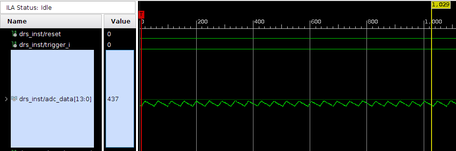
First, I do not think the noise observed is being injected from elsewhere on the board. If I run the DRS in transparent mode, the baseline noise is low, on order 3.5 mV (60 ADU), perhaps radiated from a clock. See below image. The scale is 0 to 1000 ADU with LSB = 6 uV (same AD9245 as eval board.). The DRS is in RUNNING state, I have forced a trigger in the ILA. This is for a single channel, CH0, 1024 cells.


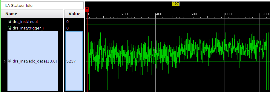
In the next image, I show the waveform obtained from a full readout. This corresponds to ADC_READOUT state, and the plot uses the same 1000 ADU scale. Noise seems around 350 ADU now, many factors worse than before.

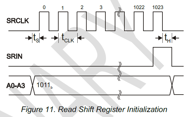
We've spent a lot of time trying to understand what's happening. One area that would be helpful to get some guidance on is the "t_samp" parameter. In Fig. 11 of the data sheet, should there be a t_samp label between t_s and t_clk? It just has arrows there with some width.


In our current firmware I believe R1 is simply one clock after R0 (for both ROI and full readout mode). Would this lead to the added noise observed in muxout?


This leads to the next question on what to actually use for t_samp. In the data sheet, page 4 "Timing Characteristics" it says to use t_samp = t0 + t_clk. Additionally, t0= 10 ns from that table. Fair enough.


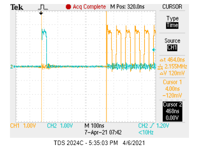
But if I check this against the eval board timing, I see very different values. Here the clock is 15 MHz so t_clk=67 ns (I note another post about this topic https://elog.psi.ch/elogs/DRS4+Forum/713), so I expect t_samp = 77 ns. But in practice it looks like the R0 to R1 delay is ~465 ns? (cyan=RSRLOAD, yellow=SRCLK)

Given this, is t_samp a value that should be tuned by the user?


Best regards,

Sean


ELOG V3.1.5-fe60aaf