 Tue Jul 7 05:13:03 2026, Jonathan Bradshaw, REFCLK input characteristics Tue Jul 7 05:13:03 2026, Jonathan Bradshaw, REFCLK input characteristics
|
Hello all
We are developing our own product with a DRS4 inside, and I'd like to get some more information about the REFCLK input. Is there any information available about:
- What's the input capacitance?
- What range of input common mode voltage (VCM) is recommended? I've been using 0.9V, but I realise that's a bit lower than the typical LVDS 1.2V. It seems to work, but might that be degrading performance, or risking reliability problems?
- What are the differential mode input high and low thresholds?
Thanks all |
Wed Jul 1 13:28:26 2026, Krzysztof Pelczar, Noise in the 2048-bin version of the eval board 
|
Hello,
I own two 2048-bin evaluation boards, bought roughly within one year (I assume no major hardware changes). The slightly newer board (sn 3102) was kept as a spare and it's performance was never fully evaluated after purchase. Now I am comparing the performance of the two boards and the newer one shows worse noise performance, despite calibrations and exactly the same working conditions (the same USB cable and port, floating inputs, firmware rev.).
Do you have any suggestions where to look for the source of such behaviour - both in the electronics and the software?
Thank you in advance for any help.
Krzysztof
PS: Measured the base frequency of the noise to be 1/512 of the sampling frequency (for 4.726 and 4.092 GHz sf). Some FPGA issue? |
|
Wed Jun 3 04:06:18 2026, Mingxin Liu, Inquiry about DC-coupled DRS4 hardware design scheme
|
Dear Dr. Stefan Ritt,
My name is Mingxin Liu. Our research group has completed a series of experimental measurements based on the available AC-coupled DRS4 evaluation board. Nevertheless, the AC-coupled input topology cannot fulfill our experimental requirements. As shown in the attached file, the existing hardware design fails to fully capture input signals featuring negative DC offset components. For this reason, we are writing to inquire about your officially recommended hardware design specifications or reference documents for DC-coupled DRS4 evaluation boards.
I look forward to any valuable suggestions and replies. Thanks in advance for your kind help.
Best regards,
Mingxin Liu |
 Fri Jun 12 08:22:30 2026, Stefan Ritt, Inquiry about DC-coupled DRS4 hardware design scheme Fri Jun 12 08:22:30 2026, Stefan Ritt, Inquiry about DC-coupled DRS4 hardware design scheme
|
We do not have any DC-coupled design for the DRS4. The reason for that is that for many applications we use SiPMs, which are directly powered through the DRS4 board. Since the bias voltage of ~50V would kill the DRS4, we always go with AC-coupling.
The reason the DRS4 evaluation board cannot fully capture signals below -0.5V is the fact that the board only has a single +5V power supply and no +-5V power rails. Having an additional -5V power rail would make the evaluation board too bulky and it could not be powered over USB.
In principle you could bias the point after the AC coupling capacitor to +5V, then you can capture up to -5V signals. Add a divider by two to go up to -10V. But then the input protection diodes won't work as it, you would need some fast 5V zener diodes which open for signals below -5V to protect the following circuitry.
Stefan |
|
Mon Jun 15 04:39:45 2026, Mingxin Liu, Inquiry about DC-coupled DRS4 hardware design scheme
|
Dear Dr. Stefan Ritt,
Thank you so much for your detailed and helpful reply. It’s very clear to me now why the standard DRS4 design uses AC coupling, and I appreciate your practical suggestions on biasing and protection.
I have a follow-up question about the THS4508 amplifier I plan to use at the input stage, if you don’t mind. If I want to make the signal path DC-coupled (both input and output), would it be possible to power the THS4508 with dual supplies, e.g., +3.5 V and -1.5 V, so that the input can accept signals in the range of -1 V to +1 V? In this configuration, could the amplifier still achieve a bandwidth of 700–800 MHz, or is that high bandwidth only guaranteed when using a single +5 V supply?
I would really appreciate your insight on this point.
Thanks again for your help and advice!
Best regards,
Mingxin Liu
| Stefan Ritt wrote: |
|
We do not have any DC-coupled design for the DRS4. The reason for that is that for many applications we use SiPMs, which are directly powered through the DRS4 board. Since the bias voltage of ~50V would kill the DRS4, we always go with AC-coupling.
The reason the DRS4 evaluation board cannot fully capture signals below -0.5V is the fact that the board only has a single +5V power supply and no +-5V power rails. Having an additional -5V power rail would make the evaluation board too bulky and it could not be powered over USB.
In principle you could bias the point after the AC coupling capacitor to +5V, then you can capture up to -5V signals. Add a divider by two to go up to -10V. But then the input protection diodes won't work as it, you would need some fast 5V zener diodes which open for signals below -5V to protect the following circuitry.
Stefan
|
|
|
Mon Jun 15 08:18:38 2026, Stefan Ritt, Inquiry about DC-coupled DRS4 hardware design scheme
|
If you DC-couple the THS4508, you risk that it's output goes to the negative rail (in your case -1.5), which would destroy the DRS4 since it's out of its specs.
To move negative signals into the posive range of 0V to 2.5V (allowed range for DRS4), the only thing I see is AC coupling with properly biasing. I don't understand why you try to do DC coupling, that will not work. Alternatively, you coudl invert your negative signal with a small inverter (usually two passive coils) which would bring a negative signal into a positive range.
Best regards,
Stefan
| Mingxin Liu wrote: |
|
Dear Dr. Stefan Ritt,
Thank you so much for your detailed and helpful reply. It’s very clear to me now why the standard DRS4 design uses AC coupling, and I appreciate your practical suggestions on biasing and protection.
I have a follow-up question about the THS4508 amplifier I plan to use at the input stage, if you don’t mind. If I want to make the signal path DC-coupled (both input and output), would it be possible to power the THS4508 with dual supplies, e.g., +3.5 V and -1.5 V, so that the input can accept signals in the range of -1 V to +1 V? In this configuration, could the amplifier still achieve a bandwidth of 700–800 MHz, or is that high bandwidth only guaranteed when using a single +5 V supply?
I would really appreciate your insight on this point.
Thanks again for your help and advice!
Best regards,
Mingxin Liu
| Stefan Ritt wrote: |
|
We do not have any DC-coupled design for the DRS4. The reason for that is that for many applications we use SiPMs, which are directly powered through the DRS4 board. Since the bias voltage of ~50V would kill the DRS4, we always go with AC-coupling.
The reason the DRS4 evaluation board cannot fully capture signals below -0.5V is the fact that the board only has a single +5V power supply and no +-5V power rails. Having an additional -5V power rail would make the evaluation board too bulky and it could not be powered over USB.
In principle you could bias the point after the AC coupling capacitor to +5V, then you can capture up to -5V signals. Add a divider by two to go up to -10V. But then the input protection diodes won't work as it, you would need some fast 5V zener diodes which open for signals below -5V to protect the following circuitry.
Stefan
|
|
|
|
Mon Jun 15 09:04:35 2026, Mingxin Liu, Inquiry about DC-coupled DRS4 hardware design scheme
|
Dear Dr. Stefan Ritt,
Thank you for your reply. My previous description was not accurate enough. We plan to modify the design referring to the attached file, and the details are as follows:
We will remove capacitor C2 to make the input DC-coupled. The signal ranging from -1 V to +1 V comes in via J1, then passes through a π-type attenuator to halve the signal amplitude before entering the amplifier. The amplifier gain is set to 2.
We are considering two dual supply options for the THS4508: +3.5 V / -1.5 V or +4 V / -1 V. The output common-mode voltage is set to 1.8 V through the CMOFS pin. After that, the signal goes through a voltage divider with 28 Ω and 22 Ω resistors.
The final signal to DRS4 has a common-mode voltage of about 0.8 V and a differential swing of -440 mV ~ +440 mV, which meets the DRS4 input requirements.
Could you please check if this THS4508 design is reasonable? We would also be grateful for any better suggestions or alternative solutions.
Thanks a lot for your support!
Best regards,
Mingxin Liu
| Stefan Ritt wrote: |
|
If you DC-couple the THS4508, you risk that it's output goes to the negative rail (in your case -1.5), which would destroy the DRS4 since it's out of its specs.
To move negative signals into the posive range of 0V to 2.5V (allowed range for DRS4), the only thing I see is AC coupling with properly biasing. I don't understand why you try to do DC coupling, that will not work. Alternatively, you coudl invert your negative signal with a small inverter (usually two passive coils) which would bring a negative signal into a positive range.
Best regards,
Stefan
| Mingxin Liu wrote: |
|
Dear Dr. Stefan Ritt,
Thank you so much for your detailed and helpful reply. It’s very clear to me now why the standard DRS4 design uses AC coupling, and I appreciate your practical suggestions on biasing and protection.
I have a follow-up question about the THS4508 amplifier I plan to use at the input stage, if you don’t mind. If I want to make the signal path DC-coupled (both input and output), would it be possible to power the THS4508 with dual supplies, e.g., +3.5 V and -1.5 V, so that the input can accept signals in the range of -1 V to +1 V? In this configuration, could the amplifier still achieve a bandwidth of 700–800 MHz, or is that high bandwidth only guaranteed when using a single +5 V supply?
I would really appreciate your insight on this point.
Thanks again for your help and advice!
Best regards,
Mingxin Liu
| Stefan Ritt wrote: |
|
We do not have any DC-coupled design for the DRS4. The reason for that is that for many applications we use SiPMs, which are directly powered through the DRS4 board. Since the bias voltage of ~50V would kill the DRS4, we always go with AC-coupling.
The reason the DRS4 evaluation board cannot fully capture signals below -0.5V is the fact that the board only has a single +5V power supply and no +-5V power rails. Having an additional -5V power rail would make the evaluation board too bulky and it could not be powered over USB.
In principle you could bias the point after the AC coupling capacitor to +5V, then you can capture up to -5V signals. Add a divider by two to go up to -10V. But then the input protection diodes won't work as it, you would need some fast 5V zener diodes which open for signals below -5V to protect the following circuitry.
Stefan
|
|
|
|
|
Mon Jun 15 10:34:33 2026, Stefan Ritt, Inquiry about DC-coupled DRS4 hardware design scheme
|
What you describe is kind of independent of the DRS4. You can just build it and see if it works before you connect it to the DRS4. I don't see any better solution.
Stefan |
|
Thu Mar 5 14:37:48 2026, QICHAOWU, Waveform Truncation Near the Cell0-Cell1023 Boundary in DRS4 ROI Readout Mode
|
Dear Dr. Stefan Ritt
I am writing to seek your advice regarding an issue I encountered while using the DRS4 chip in ROI (Region of Interest) readout mode to sample waveforms. My name is Qichao Wu, and I have been working with the DRS4 for waveform sampling.
In my setup, I input two identical sine waves (with a period of 250 ns and the same phase) into two different channels of the same DRS4 chip. Ideally, the waveforms acquired from both channels should completely overlap, as shown in Figure 1. However, I occasionally observe that the waveform from one of the channels is truncated. The truncated portion appears to originate from a different segment of the input signal, resulting in only partial overlap between the two channels. This phenomenon is illustrated in Figure 1. Additionally, there are instances where both channels exhibit truncation simultaneously, as depicted in Figure 2.
I have confirmed this issue by observing the truncated waveforms directly on an oscilloscope when the DRS4 is operated in ROI mode. Notably, the truncation points always occur near cell 0 and cell 1023 of the DRS4 switch array.
Could you kindly provide guidance on how to resolve or mitigate this issue? Any suggestions or insights you could offer would be greatly appreciated.
I look forward to your positive response and thank you in advance for your time and assistance.
Best regards,
Qichao Wu
|
|
Thu Mar 5 14:52:07 2026, Stefan Ritt, Waveform Truncation Near the Cell0-Cell1023 Boundary in DRS4 ROI Readout Mode
|
Does this happen with your own hardware or with the DRS4 evaluation board? If it's your own hardware, do you read out all 1024 bins in the ROI mode or only a partial waveforem?
| QICHAOWU wrote: |
|
Dear Dr. Stefan Ritt
I am writing to seek your advice regarding an issue I encountered while using the DRS4 chip in ROI (Region of Interest) readout mode to sample waveforms. My name is Qichao Wu, and I have been working with the DRS4 for waveform sampling.
In my setup, I input two identical sine waves (with a period of 250 ns and the same phase) into two different channels of the same DRS4 chip. Ideally, the waveforms acquired from both channels should completely overlap, as shown in Figure 1. However, I occasionally observe that the waveform from one of the channels is truncated. The truncated portion appears to originate from a different segment of the input signal, resulting in only partial overlap between the two channels. This phenomenon is illustrated in Figure 1. Additionally, there are instances where both channels exhibit truncation simultaneously, as depicted in Figure 2.
I have confirmed this issue by observing the truncated waveforms directly on an oscilloscope when the DRS4 is operated in ROI mode. Notably, the truncation points always occur near cell 0 and cell 1023 of the DRS4 switch array.
Could you kindly provide guidance on how to resolve or mitigate this issue? Any suggestions or insights you could offer would be greatly appreciated.
I look forward to your positive response and thank you in advance for your time and assistance.
Best regards,
Qichao Wu
|
|
|
Thu Mar 5 15:39:30 2026, QICHAOWU, Waveform Truncation Near the Cell0-Cell1023 Boundary in DRS4 ROI Readout Mode
|
Thank you for your prompt reply. We have developed our own DRS4-based hardware and successfully read out all 1024 bins using ROI mode. However, we are encountering the waveform truncation issue mentioned earlier. If possible, we would also like to purchase an evaluation board for reference.
| Stefan Ritt wrote: |
|
Does this happen with your own hardware or with the DRS4 evaluation board? If it's your own hardware, do you read out all 1024 bins in the ROI mode or only a partial waveforem?
| QICHAOWU wrote: |
|
Dear Dr. Stefan Ritt
I am writing to seek your advice regarding an issue I encountered while using the DRS4 chip in ROI (Region of Interest) readout mode to sample waveforms. My name is Qichao Wu, and I have been working with the DRS4 for waveform sampling.
In my setup, I input two identical sine waves (with a period of 250 ns and the same phase) into two different channels of the same DRS4 chip. Ideally, the waveforms acquired from both channels should completely overlap, as shown in Figure 1. However, I occasionally observe that the waveform from one of the channels is truncated. The truncated portion appears to originate from a different segment of the input signal, resulting in only partial overlap between the two channels. This phenomenon is illustrated in Figure 1. Additionally, there are instances where both channels exhibit truncation simultaneously, as depicted in Figure 2.
I have confirmed this issue by observing the truncated waveforms directly on an oscilloscope when the DRS4 is operated in ROI mode. Notably, the truncation points always occur near cell 0 and cell 1023 of the DRS4 switch array.
Could you kindly provide guidance on how to resolve or mitigate this issue? Any suggestions or insights you could offer would be greatly appreciated.
I look forward to your positive response and thank you in advance for your time and assistance.
Best regards,
Qichao Wu
|
|
|
|
Fri Mar 27 09:56:06 2026, Stefan Ritt, Waveform Truncation Near the Cell0-Cell1023 Boundary in DRS4 ROI Readout Mode
|
Actually looking at your waveforms again, I think I understand maybe your problem. You stop the DRS4 randomly, but your ROI readout mode does not really work. Seems like you always read from the first cell, or just from a wrong cell. Since your sine wave period is not a multiple of the readout window, you see a phase jump between the beginning of your sampling window and the end of your sampling window. The little spikes before and after the jump are normal, since the first and last samples of the DRS4 readout might have some offset. Check that your FPGA really uses RSLOAD to start the readout, and not the "full readout".
The evaluation board might really help you, since you can compare 1:1 all control signals with yours.
Stefan
| QICHAOWU wrote: |
|
Dear Dr. Stefan Ritt
I am writing to seek your advice regarding an issue I encountered while using the DRS4 chip in ROI (Region of Interest) readout mode to sample waveforms. My name is Qichao Wu, and I have been working with the DRS4 for waveform sampling.
In my setup, I input two identical sine waves (with a period of 250 ns and the same phase) into two different channels of the same DRS4 chip. Ideally, the waveforms acquired from both channels should completely overlap, as shown in Figure 1. However, I occasionally observe that the waveform from one of the channels is truncated. The truncated portion appears to originate from a different segment of the input signal, resulting in only partial overlap between the two channels. This phenomenon is illustrated in Figure 1. Additionally, there are instances where both channels exhibit truncation simultaneously, as depicted in Figure 2.
I have confirmed this issue by observing the truncated waveforms directly on an oscilloscope when the DRS4 is operated in ROI mode. Notably, the truncation points always occur near cell 0 and cell 1023 of the DRS4 switch array.
Could you kindly provide guidance on how to resolve or mitigate this issue? Any suggestions or insights you could offer would be greatly appreciated.
I look forward to your positive response and thank you in advance for your time and assistance.
Best regards,
Qichao Wu
|
|
|
Fri Apr 17 10:54:20 2026, QICHAOWU, Waveform Truncation Near the Cell0-Cell1023 Boundary in DRS4 ROI Readout Mode
|
Dear Dr.Stefan
Thank you for your detailed response. Following your suggestion, I used an oscilloscope to observe the RSLOAD and SRCLK signals, and they conform to the readout timing described in the datasheet.
I can now confirm that the DRS4 occasionally fails to correctly update the stop position to cell 1023, or the stored waveform from cell 0 to the stop position is corrupted. As a result, part of the waveform comes from the most recent acquisition while the other part comes from an earlier one, causing the truncation I observed. This issue occurs with a certain probability—more than half of the acquisitions still yield complete, continuous waveforms.
Interestingly, when I use the same FPGA code and host software on the DRS4 evaluation board, no truncation occurs at all. I am currently comparing the behavior of the two setups from both hardware and software perspectives. Could you kindly provide some suggestions on further tests I could perform?
Thank you very much for your help.
Best regards,
Qichao Wu
| Stefan Ritt wrote: |
|
Actually looking at your waveforms again, I think I understand maybe your problem. You stop the DRS4 randomly, but your ROI readout mode does not really work. Seems like you always read from the first cell, or just from a wrong cell. Since your sine wave period is not a multiple of the readout window, you see a phase jump between the beginning of your sampling window and the end of your sampling window. The little spikes before and after the jump are normal, since the first and last samples of the DRS4 readout might have some offset. Check that your FPGA really uses RSLOAD to start the readout, and not the "full readout".
The evaluation board might really help you, since you can compare 1:1 all control signals with yours.
Stefan
| QICHAOWU wrote: |
|
Dear Dr. Stefan Ritt
I am writing to seek your advice regarding an issue I encountered while using the DRS4 chip in ROI (Region of Interest) readout mode to sample waveforms. My name is Qichao Wu, and I have been working with the DRS4 for waveform sampling.
In my setup, I input two identical sine waves (with a period of 250 ns and the same phase) into two different channels of the same DRS4 chip. Ideally, the waveforms acquired from both channels should completely overlap, as shown in Figure 1. However, I occasionally observe that the waveform from one of the channels is truncated. The truncated portion appears to originate from a different segment of the input signal, resulting in only partial overlap between the two channels. This phenomenon is illustrated in Figure 1. Additionally, there are instances where both channels exhibit truncation simultaneously, as depicted in Figure 2.
I have confirmed this issue by observing the truncated waveforms directly on an oscilloscope when the DRS4 is operated in ROI mode. Notably, the truncation points always occur near cell 0 and cell 1023 of the DRS4 switch array.
Could you kindly provide guidance on how to resolve or mitigate this issue? Any suggestions or insights you could offer would be greatly appreciated.
I look forward to your positive response and thank you in advance for your time and assistance.
Best regards,
Qichao Wu
|
|
|
|
Fri Apr 17 12:39:11 2026, Stefan Ritt, Waveform Truncation Near the Cell0-Cell1023 Boundary in DRS4 ROI Readout Mode
|
Not much I can say here. I know that the DRS4 works reliably, since we have an experiment here with 500 chips running since 5 years and we did not observer what you described. Therefore, it must be some subtle detail of your FPGA code or the voltage levels on your board. As I said, what I would do is to get the evaluation abord and copare signals 1:1.
Stefan
| QICHAOWU wrote: |
|
Dear Dr.Stefan
Thank you for your detailed response. Following your suggestion, I used an oscilloscope to observe the RSLOAD and SRCLK signals, and they conform to the readout timing described in the datasheet.
I can now confirm that the DRS4 occasionally fails to correctly update the stop position to cell 1023, or the stored waveform from cell 0 to the stop position is corrupted. As a result, part of the waveform comes from the most recent acquisition while the other part comes from an earlier one, causing the truncation I observed. This issue occurs with a certain probability—more than half of the acquisitions still yield complete, continuous waveforms.
Interestingly, when I use the same FPGA code and host software on the DRS4 evaluation board, no truncation occurs at all. I am currently comparing the behavior of the two setups from both hardware and software perspectives. Could you kindly provide some suggestions on further tests I could perform?
Thank you very much for your help.
Best regards,
Qichao Wu
| Stefan Ritt wrote: |
|
Actually looking at your waveforms again, I think I understand maybe your problem. You stop the DRS4 randomly, but your ROI readout mode does not really work. Seems like you always read from the first cell, or just from a wrong cell. Since your sine wave period is not a multiple of the readout window, you see a phase jump between the beginning of your sampling window and the end of your sampling window. The little spikes before and after the jump are normal, since the first and last samples of the DRS4 readout might have some offset. Check that your FPGA really uses RSLOAD to start the readout, and not the "full readout".
The evaluation board might really help you, since you can compare 1:1 all control signals with yours.
Stefan
| QICHAOWU wrote: |
|
Dear Dr. Stefan Ritt
I am writing to seek your advice regarding an issue I encountered while using the DRS4 chip in ROI (Region of Interest) readout mode to sample waveforms. My name is Qichao Wu, and I have been working with the DRS4 for waveform sampling.
In my setup, I input two identical sine waves (with a period of 250 ns and the same phase) into two different channels of the same DRS4 chip. Ideally, the waveforms acquired from both channels should completely overlap, as shown in Figure 1. However, I occasionally observe that the waveform from one of the channels is truncated. The truncated portion appears to originate from a different segment of the input signal, resulting in only partial overlap between the two channels. This phenomenon is illustrated in Figure 1. Additionally, there are instances where both channels exhibit truncation simultaneously, as depicted in Figure 2.
I have confirmed this issue by observing the truncated waveforms directly on an oscilloscope when the DRS4 is operated in ROI mode. Notably, the truncation points always occur near cell 0 and cell 1023 of the DRS4 switch array.
Could you kindly provide guidance on how to resolve or mitigate this issue? Any suggestions or insights you could offer would be greatly appreciated.
I look forward to your positive response and thank you in advance for your time and assistance.
Best regards,
Qichao Wu
|
|
|
|
|
Tue Apr 28 04:40:38 2026, QICHAOWU, Waveform Truncation Near the Cell0-Cell1023 Boundary in DRS4 ROI Readout Mode
|
Dear Dr. Stefan Ritt,
I am writing to express my sincere gratitude for your continued and prompt responses to our previous inquiries regarding the waveform truncation issue with the DRS4. Your advice and insights have been invaluable throughout this debugging process.
We have now preliminarily identified and resolved the problem. The key observation came when we powered the DRS4 from an independent supply: shortly after power‑up, with both DENABLE and DWRITE pulled low to GND, the VDD rail still drew an abnormally high current (approximately 1.8 A). This indicated that the DRS4 had been unintentionally activated into an abnormal state. While we confirmed with both an oscilloscope and a multimeter that the DENABLE and DWRITE pins remained at a valid low level, we suspected that the chip’s initialization was corrupted, preventing the internal registers from being loaded with their default values.
To address this, we manually reloaded the default register values via the FPGA. After this modification, the waveform truncation phenomenon completely disappeared.
Thus, we conclude that the root cause of the waveform truncation was improper initialization of the DRS4. Going forward, we will continue to improve the hardware conditions to ensure correct initialization of the chip.
Thank you once again, Dr. Ritt, for your active and generous support. We hope that the problem we encountered and the solution we found will be helpful to other DRS4 users and contribute to the healthy development of the DRS4 community.
| Stefan Ritt wrote: |
|
Not much I can say here. I know that the DRS4 works reliably, since we have an experiment here with 500 chips running since 5 years and we did not observer what you described. Therefore, it must be some subtle detail of your FPGA code or the voltage levels on your board. As I said, what I would do is to get the evaluation abord and copare signals 1:1.
Stefan
| QICHAOWU wrote: |
|
Dear Dr.Stefan
Thank you for your detailed response. Following your suggestion, I used an oscilloscope to observe the RSLOAD and SRCLK signals, and they conform to the readout timing described in the datasheet.
I can now confirm that the DRS4 occasionally fails to correctly update the stop position to cell 1023, or the stored waveform from cell 0 to the stop position is corrupted. As a result, part of the waveform comes from the most recent acquisition while the other part comes from an earlier one, causing the truncation I observed. This issue occurs with a certain probability—more than half of the acquisitions still yield complete, continuous waveforms.
Interestingly, when I use the same FPGA code and host software on the DRS4 evaluation board, no truncation occurs at all. I am currently comparing the behavior of the two setups from both hardware and software perspectives. Could you kindly provide some suggestions on further tests I could perform?
Thank you very much for your help.
Best regards,
Qichao Wu
| Stefan Ritt wrote: |
|
Actually looking at your waveforms again, I think I understand maybe your problem. You stop the DRS4 randomly, but your ROI readout mode does not really work. Seems like you always read from the first cell, or just from a wrong cell. Since your sine wave period is not a multiple of the readout window, you see a phase jump between the beginning of your sampling window and the end of your sampling window. The little spikes before and after the jump are normal, since the first and last samples of the DRS4 readout might have some offset. Check that your FPGA really uses RSLOAD to start the readout, and not the "full readout".
The evaluation board might really help you, since you can compare 1:1 all control signals with yours.
Stefan
| QICHAOWU wrote: |
|
Dear Dr. Stefan Ritt
I am writing to seek your advice regarding an issue I encountered while using the DRS4 chip in ROI (Region of Interest) readout mode to sample waveforms. My name is Qichao Wu, and I have been working with the DRS4 for waveform sampling.
In my setup, I input two identical sine waves (with a period of 250 ns and the same phase) into two different channels of the same DRS4 chip. Ideally, the waveforms acquired from both channels should completely overlap, as shown in Figure 1. However, I occasionally observe that the waveform from one of the channels is truncated. The truncated portion appears to originate from a different segment of the input signal, resulting in only partial overlap between the two channels. This phenomenon is illustrated in Figure 1. Additionally, there are instances where both channels exhibit truncation simultaneously, as depicted in Figure 2.
I have confirmed this issue by observing the truncated waveforms directly on an oscilloscope when the DRS4 is operated in ROI mode. Notably, the truncation points always occur near cell 0 and cell 1023 of the DRS4 switch array.
Could you kindly provide guidance on how to resolve or mitigate this issue? Any suggestions or insights you could offer would be greatly appreciated.
I look forward to your positive response and thank you in advance for your time and assistance.
Best regards,
Qichao Wu
|
|
|
|
|
|
Tue Apr 28 08:15:35 2026, Stefan Ritt, Waveform Truncation Near the Cell0-Cell1023 Boundary in DRS4 ROI Readout Mode
|
The DRS4 gets into the "1.8A" state if DSPEED approaches like 0.7V. Then both inverters of the Domino chain are kind of open and a large current flows. In that state, the only way out is a power cycle.
It's however not clear to me how you get there. If DENABLE is low, this should be prevented. Most FPGAs however pull up their pins on power-on, and ony when configured, the pins go low according to the programming. Maybe it's the time during the FPGA boot which is your problem. Some FPGAs can be configured not to do this. I woulld recommend putting VDD analog, VDD digital, DSPEED, DENABLE, FPGA config ready, all on an oscilloscope and watch what happens during power on. The 1.8A state should be prevented by all means since it could damage the chip.
Stefan |
|
Mon Aug 18 06:52:51 2025, Jonathan Bradshaw, Unexpected behaviour following RSRLOAD
|
Hello
I'm working to bring up a new capture board using a DRS4 and I'm having a minor problem and a major problem.
Minor problem: if I send a reset signal into the DRS4, the PLL doesn't work right. If I leave NRSESET pin with a wek pullup (and never 'manually' reset the DRS4) it runs OK. Is there some minimum time I need to observe between sending a NRESET pulse and setting DENABLE high to start the PLL?
Major problem: I can't get the stop position.
What am I doing?
- Set DENABLE high
- Wait until DRS capture is requested (seconds to minutes)
- Configure Write Shift Register with 0b01010101
- Configure Write Control Register with 0b11111111
- Fill the Read Shift Register with 1024x '0's
- Set DWRITE high
- Await trigger (some milliseconds). During this phase address = 0b1011
- Set DWRITE low
- Wait ~ 40 ns
- Set address = 0b1101
- Wait ~ 150 us
- Pulse RSRLOAD high for 30 ns
- Wait 30 ns
- Sample SROUT to get top bit of Write Shift Register
- Set address = 0b0000
- Wait ~ 350 ns
- Begin clocking out analog samples
What's going wrong?
- When I look at the first 10 bits out of SROUT, I should see stop positions. However, these bits are almost always zero (I get 7 bits which are always 0 followed by 3 bits which are sometimes ones)
- When I probe the WSROUT pin (and remembering that DWRITE is low at this point), I expected to see a single one bit coming out of the read shift register as I apply 1024 pulses to SRCLK. Instead, I am seeing two set bits coming out of the read shift register
- When I plot the captured analog waveform it's a mess - it seems like 2 analog output buffers are enabling at once and fighting over the output voltage
Do you have any suggestions or warnings about proper deployment of the RSRLOAD pin?
I left this a bit late in my day for posting, so I'll need to follow up with some 'scope captures tomorrow. |
|
Tue Aug 19 02:40:58 2025, Jonathan Bradshaw, Unexpected behaviour following RSRLOAD 6x
|
Some images
Notes:
- top of the puicture shows the logic channels
- Red: SRCLK
- Blue: SRIN
- Green: SROUT
- Orange: normally WSROUT, but swapped to RSRLOAD for last picture
| Jonathan Bradshaw wrote: |
|
Hello
I'm working to bring up a new capture board using a DRS4 and I'm having a minor problem and a major problem.
Minor problem: if I send a reset signal into the DRS4, the PLL doesn't work right. If I leave NRSESET pin with a wek pullup (and never 'manually' reset the DRS4) it runs OK. Is there some minimum time I need to observe between sending a NRESET pulse and setting DENABLE high to start the PLL?
Major problem: I can't get the stop position.
What am I doing?
- Set DENABLE high
- Wait until DRS capture is requested (seconds to minutes)
- Configure Write Shift Register with 0b01010101
- Configure Write Control Register with 0b11111111
- Fill the Read Shift Register with 1024x '0's
- Set DWRITE high
- Await trigger (some milliseconds). During this phase address = 0b1011
- Set DWRITE low
- Wait ~ 40 ns
- Set address = 0b1101
- Wait ~ 150 us
- Pulse RSRLOAD high for 30 ns
- Wait 30 ns
- Sample SROUT to get top bit of Write Shift Register
- Set address = 0b0000
- Wait ~ 350 ns
- Begin clocking out analog samples
What's going wrong?
- When I look at the first 10 bits out of SROUT, I should see stop positions. However, these bits are almost always zero (I get 7 bits which are always 0 followed by 3 bits which are sometimes ones)
- When I probe the WSROUT pin (and remembering that DWRITE is low at this point), I expected to see a single one bit coming out of the read shift register as I apply 1024 pulses to SRCLK. Instead, I am seeing two set bits coming out of the read shift register
- When I plot the captured analog waveform it's a mess - it seems like 2 analog output buffers are enabling at once and fighting over the output voltage
Do you have any suggestions or warnings about proper deployment of the RSRLOAD pin?
I left this a bit late in my day for posting, so I'll need to follow up with some 'scope captures tomorrow.
|
|
|
Tue Aug 19 23:10:30 2025, Jonathan Bradshaw, Unexpected behaviour following RSRLOAD
|
Turns out it was a damaged DRS4 IC.
I ported the drs4_eval5_app code onto our board and observed much the same misbehaviour. So I bit the bullet and replaced the DRS4 IC, and things are going better.
| Jonathan Bradshaw wrote: |
|
Some images
Notes:
- top of the puicture shows the logic channels
- Red: SRCLK
- Blue: SRIN
- Green: SROUT
- Orange: normally WSROUT, but swapped to RSRLOAD for last picture
| Jonathan Bradshaw wrote: |
|
Hello
I'm working to bring up a new capture board using a DRS4 and I'm having a minor problem and a major problem.
Minor problem: if I send a reset signal into the DRS4, the PLL doesn't work right. If I leave NRSESET pin with a wek pullup (and never 'manually' reset the DRS4) it runs OK. Is there some minimum time I need to observe between sending a NRESET pulse and setting DENABLE high to start the PLL?
Major problem: I can't get the stop position.
What am I doing?
- Set DENABLE high
- Wait until DRS capture is requested (seconds to minutes)
- Configure Write Shift Register with 0b01010101
- Configure Write Control Register with 0b11111111
- Fill the Read Shift Register with 1024x '0's
- Set DWRITE high
- Await trigger (some milliseconds). During this phase address = 0b1011
- Set DWRITE low
- Wait ~ 40 ns
- Set address = 0b1101
- Wait ~ 150 us
- Pulse RSRLOAD high for 30 ns
- Wait 30 ns
- Sample SROUT to get top bit of Write Shift Register
- Set address = 0b0000
- Wait ~ 350 ns
- Begin clocking out analog samples
What's going wrong?
- When I look at the first 10 bits out of SROUT, I should see stop positions. However, these bits are almost always zero (I get 7 bits which are always 0 followed by 3 bits which are sometimes ones)
- When I probe the WSROUT pin (and remembering that DWRITE is low at this point), I expected to see a single one bit coming out of the read shift register as I apply 1024 pulses to SRCLK. Instead, I am seeing two set bits coming out of the read shift register
- When I plot the captured analog waveform it's a mess - it seems like 2 analog output buffers are enabling at once and fighting over the output voltage
Do you have any suggestions or warnings about proper deployment of the RSRLOAD pin?
I left this a bit late in my day for posting, so I'll need to follow up with some 'scope captures tomorrow.
|
|
|
|
Sat Jul 5 04:36:13 2025, Sandeep Godiyal, Wrong Firmware Version: board has 13279, required is 15147. Board may not work properly
|
I am using DRS4 Evaluation Board Rev.: 2.0.. Command Line interface: "drscl" detecting the board with message: Found DRS4 board 0 on USB, serial #2034, firmware revision 13279, also info command also working.
In "drsosc" interface: Getting this message: Wrong Firmware Version: board has 13279, required is 15147. Board may not work properly. In "config" I checked it is detecting the board.
Software version, I am using is: "drs505.exe"
How can I resolve these issues, please guide! |
|
Mon Jul 7 16:53:26 2025, Stefan Ritt, Wrong Firmware Version: board has 13279, required is 15147. Board may not work properly
|
You have to use the software belonging to that board. You cannot use the newest software with an old board. Look here:
https://www.psi.ch/en/ltp-muon-physics/software-download
So you need teh software version 2.0.
/Stefan
|
|
Thu May 8 23:41:03 2025, Jonathan Bradshaw, Handling of Write Shift Register and Write Config Register
|
Hi all
We're building a product which will use two different operating modes; firstly a long capcture using channel daisy chaining (2048 samples) and secondly a segmented capture (2 separate captures of 1024 samples each).
For the long capture, I'm looking to capture 2048 samples for 4 channels. Therefore I configure the Write Shift Register to 0b01010101 and the Write Config Register to 0b11111111. During capture with DWRITE=1 the Write Shift Register will update. Am I correct that once the capture is done and DWRITE=0, I can set A3..0 to 0b1101 and simply read the value of WSROUT to tell the difference?
For the segmented capture, I'm looking to capture 1024 samples for 4 channels on a first tirgger pulse, followed by 1024 samples for 4 channels on a second pulse. Therefore I configure the Write Shift Register to 0b11111111 and the Write Config Register to 0b01010101 and set DWRITE=0 to capture. After the first trigger I set DWRITE=0 and need to update the Write Config Register. Do I need to write in a whole 8 bits to the Write Config Register (i.e. 0b10101010), or can I just shift in a single new bit (value 0b0)? |
|
Fri May 9 08:17:50 2025, Stefan Ritt, Handling of Write Shift Register and Write Config Register
|
This is correct. Setting A0-A3 to 0b1101 multiplexes the Shift Write Register to SROUT, so you will either a "0" or a "1" depending on which of the two channels was written last.
Your segmented capture does unfortunately not work. Due to a bug in the silicon, the first (e.g. even) written channel gets half overwritten when you start sampling the second (odd) channel. I should remove that from the documentation.
Furthermore, reading the chip while writing on the "other side" introduces quite some additional noise. The recommended way to do simultaneous reading and writing is therefore to use two separate DRS4 chips and split the input signals to both chips, then read from one chip while writing to the other chip. This keeps the crosstalk at a minimum and both chips run at full performance.
Stefan
| Jonathan Bradshaw wrote: |
|
Hi all
We're building a product which will use two different operating modes; firstly a long capcture using channel daisy chaining (2048 samples) and secondly a segmented capture (2 separate captures of 1024 samples each).
For the long capture, I'm looking to capture 2048 samples for 4 channels. Therefore I configure the Write Shift Register to 0b01010101 and the Write Config Register to 0b11111111. During capture with DWRITE=1 the Write Shift Register will update. Am I correct that once the capture is done and DWRITE=0, I can set A3..0 to 0b1101 and simply read the value of WSROUT to tell the difference?
For the segmented capture, I'm looking to capture 1024 samples for 4 channels on a first tirgger pulse, followed by 1024 samples for 4 channels on a second pulse. Therefore I configure the Write Shift Register to 0b11111111 and the Write Config Register to 0b01010101 and set DWRITE=0 to capture. After the first trigger I set DWRITE=0 and need to update the Write Config Register. Do I need to write in a whole 8 bits to the Write Config Register (i.e. 0b10101010), or can I just shift in a single new bit (value 0b0)?
|
|
|
Tue May 13 04:10:30 2025, Jonathan Bradshaw, Handling of Write Shift Register and Write Config Register
|
Hi Stefan
Just so I'm 100% clear; is there no reliable way to perform 2 segmented captures with a single DRS4 IC?
While not a showstopper, this is a bit disappointing.
| Stefan Ritt wrote: |
|
This is correct. Setting A0-A3 to 0b1101 multiplexes the Shift Write Register to SROUT, so you will either a "0" or a "1" depending on which of the two channels was written last.
Your segmented capture does unfortunately not work. Due to a bug in the silicon, the first (e.g. even) written channel gets half overwritten when you start sampling the second (odd) channel. I should remove that from the documentation.
Furthermore, reading the chip while writing on the "other side" introduces quite some additional noise. The recommended way to do simultaneous reading and writing is therefore to use two separate DRS4 chips and split the input signals to both chips, then read from one chip while writing to the other chip. This keeps the crosstalk at a minimum and both chips run at full performance.
Stefan
| Jonathan Bradshaw wrote: |
|
Hi all
We're building a product which will use two different operating modes; firstly a long capcture using channel daisy chaining (2048 samples) and secondly a segmented capture (2 separate captures of 1024 samples each).
For the long capture, I'm looking to capture 2048 samples for 4 channels. Therefore I configure the Write Shift Register to 0b01010101 and the Write Config Register to 0b11111111. During capture with DWRITE=1 the Write Shift Register will update. Am I correct that once the capture is done and DWRITE=0, I can set A3..0 to 0b1101 and simply read the value of WSROUT to tell the difference?
For the segmented capture, I'm looking to capture 1024 samples for 4 channels on a first tirgger pulse, followed by 1024 samples for 4 channels on a second pulse. Therefore I configure the Write Shift Register to 0b11111111 and the Write Config Register to 0b01010101 and set DWRITE=0 to capture. After the first trigger I set DWRITE=0 and need to update the Write Config Register. Do I need to write in a whole 8 bits to the Write Config Register (i.e. 0b10101010), or can I just shift in a single new bit (value 0b0)?
|
|
|
|
Tue May 13 08:51:34 2025, Stefan Ritt, Handling of Write Shift Register and Write Config Register
|
Yes this is correct. Anyhow, even if it would be working, you would not be happy with it. After having designed ~10 boards with the DRS4 chip, I learned the hard way that any digital activity on the board during the sampling phase is strictly forbidden. You see crosstalk up to 100's of mV in some cases (with a preamplifier on the board, 10-20mV without preamp). So rule #1 is to keep the board as "quite" as possible when sampling the input. If you would readout the odd channels of the DRS4 during sampling of the even channels, you would probably get so much crosstalk that the samples are almost unusable. Even if you would do this with two DRS4 chips next to each other, you have to make sure to put proper grounding between the two chips, and operate them completely independent (like each one has it's onw contol lines going to the FPGA). Designing such boards is not so easy and takes lots of experience from the layouter.
Stefan
| Jonathan Bradshaw wrote: |
|
Hi Stefan
Just so I'm 100% clear; is there no reliable way to perform 2 segmented captures with a single DRS4 IC?
While not a showstopper, this is a bit disappointing.
| Stefan Ritt wrote: |
|
This is correct. Setting A0-A3 to 0b1101 multiplexes the Shift Write Register to SROUT, so you will either a "0" or a "1" depending on which of the two channels was written last.
Your segmented capture does unfortunately not work. Due to a bug in the silicon, the first (e.g. even) written channel gets half overwritten when you start sampling the second (odd) channel. I should remove that from the documentation.
Furthermore, reading the chip while writing on the "other side" introduces quite some additional noise. The recommended way to do simultaneous reading and writing is therefore to use two separate DRS4 chips and split the input signals to both chips, then read from one chip while writing to the other chip. This keeps the crosstalk at a minimum and both chips run at full performance.
Stefan
| Jonathan Bradshaw wrote: |
|
Hi all
We're building a product which will use two different operating modes; firstly a long capcture using channel daisy chaining (2048 samples) and secondly a segmented capture (2 separate captures of 1024 samples each).
For the long capture, I'm looking to capture 2048 samples for 4 channels. Therefore I configure the Write Shift Register to 0b01010101 and the Write Config Register to 0b11111111. During capture with DWRITE=1 the Write Shift Register will update. Am I correct that once the capture is done and DWRITE=0, I can set A3..0 to 0b1101 and simply read the value of WSROUT to tell the difference?
For the segmented capture, I'm looking to capture 1024 samples for 4 channels on a first tirgger pulse, followed by 1024 samples for 4 channels on a second pulse. Therefore I configure the Write Shift Register to 0b11111111 and the Write Config Register to 0b01010101 and set DWRITE=0 to capture. After the first trigger I set DWRITE=0 and need to update the Write Config Register. Do I need to write in a whole 8 bits to the Write Config Register (i.e. 0b10101010), or can I just shift in a single new bit (value 0b0)?
|
|
|
|
|
Thu May 15 00:01:20 2025, Jonathan Bradshaw, Handling of Write Shift Register and Write Config Register
|
All right, thank you for the clarification.
| Stefan Ritt wrote: |
|
Yes this is correct. Anyhow, even if it would be working, you would not be happy with it. After having designed ~10 boards with the DRS4 chip, I learned the hard way that any digital activity on the board during the sampling phase is strictly forbidden. You see crosstalk up to 100's of mV in some cases (with a preamplifier on the board, 10-20mV without preamp). So rule #1 is to keep the board as "quite" as possible when sampling the input. If you would readout the odd channels of the DRS4 during sampling of the even channels, you would probably get so much crosstalk that the samples are almost unusable. Even if you would do this with two DRS4 chips next to each other, you have to make sure to put proper grounding between the two chips, and operate them completely independent (like each one has it's onw contol lines going to the FPGA). Designing such boards is not so easy and takes lots of experience from the layouter.
Stefan
| Jonathan Bradshaw wrote: |
|
Hi Stefan
Just so I'm 100% clear; is there no reliable way to perform 2 segmented captures with a single DRS4 IC?
While not a showstopper, this is a bit disappointing.
| Stefan Ritt wrote: |
|
This is correct. Setting A0-A3 to 0b1101 multiplexes the Shift Write Register to SROUT, so you will either a "0" or a "1" depending on which of the two channels was written last.
Your segmented capture does unfortunately not work. Due to a bug in the silicon, the first (e.g. even) written channel gets half overwritten when you start sampling the second (odd) channel. I should remove that from the documentation.
Furthermore, reading the chip while writing on the "other side" introduces quite some additional noise. The recommended way to do simultaneous reading and writing is therefore to use two separate DRS4 chips and split the input signals to both chips, then read from one chip while writing to the other chip. This keeps the crosstalk at a minimum and both chips run at full performance.
Stefan
| Jonathan Bradshaw wrote: |
|
Hi all
We're building a product which will use two different operating modes; firstly a long capcture using channel daisy chaining (2048 samples) and secondly a segmented capture (2 separate captures of 1024 samples each).
For the long capture, I'm looking to capture 2048 samples for 4 channels. Therefore I configure the Write Shift Register to 0b01010101 and the Write Config Register to 0b11111111. During capture with DWRITE=1 the Write Shift Register will update. Am I correct that once the capture is done and DWRITE=0, I can set A3..0 to 0b1101 and simply read the value of WSROUT to tell the difference?
For the segmented capture, I'm looking to capture 1024 samples for 4 channels on a first tirgger pulse, followed by 1024 samples for 4 channels on a second pulse. Therefore I configure the Write Shift Register to 0b11111111 and the Write Config Register to 0b01010101 and set DWRITE=0 to capture. After the first trigger I set DWRITE=0 and need to update the Write Config Register. Do I need to write in a whole 8 bits to the Write Config Register (i.e. 0b10101010), or can I just shift in a single new bit (value 0b0)?
|
|
|
|
|
|
Thu May 8 23:23:19 2025, Jonathan Bradshaw, Clarification of full channel readout
|
Hi all
We're working on a new product using the DRS4 IC, and want to do a full readout from cell 0 (not just Region of Interest). I have a couple of questions I hope you can help me with:
- We plan to do a full readout sequence, starting at cell 0. Part of that sequence includes pulsing RSRLOAD and reading out the stop position as shown in v0.9 datasheet Figure 15. What should the DRS4 address bits A3..0 be set to for reading out the stop position? (I’m assuming it’s 1011 ‘Address Read Shift Register’)
- What is the output delay from the falling edge of SRCLK to valid data at SROUT?
- For channel readout, we pulse SRCLK to advance the read shift register. The diagram shown in v0.9 datasheet Figure 12 appears to show that the analog output is updated on the rising edge of SRCLK. Is this correct or have I misread the diagram? (Other shift register transfers are clocked on the falling edge
- The DRS4 v0.9 datasheet Figure 7 shows that the Configuration register is clocked on the falling edge of SRCLK. Just below that is the text “The new register content becomes immediately active at the eighth rising edge of the SRCLK signal.” Should that perhaps read ‘… the eighth falling edge of the SRCLK signal’?
|
|
Fri May 9 08:26:17 2025, Stefan Ritt, Clarification of full channel readout
|
The full readout mode is not really recommended since you have to pull out the stop position separately. Just do the ROI readout using the RSRLOAD signal, and then do 1024 samples, which also gives you the full waveform, but also the stop position in a single readout cyclce. The "full readout mode" is more there for "historical reasons", but nobody really uses it any more.
If you are interested in all details of the control signals, I propose you have a look at the VHDL code which comes with the software distribution. It's contained in the "firmware" subdirectoy and called drs4_eval5_app.vhd
Stefan
| Jonathan Bradshaw wrote: |
|
Hi all
We're working on a new product using the DRS4 IC, and want to do a full readout from cell 0 (not just Region of Interest). I have a couple of questions I hope you can help me with:
- We plan to do a full readout sequence, starting at cell 0. Part of that sequence includes pulsing RSRLOAD and reading out the stop position as shown in v0.9 datasheet Figure 15. What should the DRS4 address bits A3..0 be set to for reading out the stop position? (I’m assuming it’s 1011 ‘Address Read Shift Register’)
- What is the output delay from the falling edge of SRCLK to valid data at SROUT?
- For channel readout, we pulse SRCLK to advance the read shift register. The diagram shown in v0.9 datasheet Figure 12 appears to show that the analog output is updated on the rising edge of SRCLK. Is this correct or have I misread the diagram? (Other shift register transfers are clocked on the falling edge
- The DRS4 v0.9 datasheet Figure 7 shows that the Configuration register is clocked on the falling edge of SRCLK. Just below that is the text “The new register content becomes immediately active at the eighth rising edge of the SRCLK signal.” Should that perhaps read ‘… the eighth falling edge of the SRCLK signal’?
|
|
|
Tue Mar 25 16:31:41 2025, Matías Tobar, drs_exam.cpp not compile
|
Hi! i'm trying to compile drs_exam.cpp but it yields the following error lines:
I do have the "DRS.h" file on the same folder, which is clearly the file that's causing troubles. I also tried to run "DRS.cpp" but it yields a similar error lines. ('sin definir' means 'not defined').
Thanks a lot for the help!
$ g++ drs_exam.cpp -o drs_exam
/usr/bin/ld: /tmp/ccroK16H.o: en la función `main':
drs_exam.cpp:(.text+0x48): referencia a `DRS::DRS()' sin definir
/usr/bin/ld: drs_exam.cpp:(.text+0x135): referencia a `DRSBoard::Init()' sin definir
/usr/bin/ld: drs_exam.cpp:(.text+0x155): referencia a `DRSBoard::SetFrequency(double, bool)' sin definir
/usr/bin/ld: drs_exam.cpp:(.text+0x169): referencia a `DRSBoard::SetTranspMode(int)' sin definir
/usr/bin/ld: drs_exam.cpp:(.text+0x184): referencia a `DRSBoard::SetInputRange(double)' sin definir
/usr/bin/ld: drs_exam.cpp:(.text+0x1b6): referencia a `DRSBoard::EnableTrigger(int, int)' sin definir
/usr/bin/ld: drs_exam.cpp:(.text+0x1ca): referencia a `DRSBoard::SetTriggerConfig(int)' sin definir
/usr/bin/ld: drs_exam.cpp:(.text+0x1fe): referencia a `DRSBoard::EnableTrigger(int, int)' sin definir
/usr/bin/ld: drs_exam.cpp:(.text+0x212): referencia a `DRSBoard::SetTriggerConfig(int)' sin definir
/usr/bin/ld: drs_exam.cpp:(.text+0x22d): referencia a `DRSBoard::SetTriggerLevel(double)' sin definir
/usr/bin/ld: drs_exam.cpp:(.text+0x241): referencia a `DRSBoard::SetTriggerPolarity(bool)' sin definir
/usr/bin/ld: drs_exam.cpp:(.text+0x255): referencia a `DRSBoard::SetTriggerDelayNs(int)' sin definir
/usr/bin/ld: drs_exam.cpp:(.text+0x2b6): referencia a `DRSBoard::StartDomino()' sin definir
/usr/bin/ld: drs_exam.cpp:(.text+0x2e9): referencia a `DRSBoard::IsBusy()' sin definir
/usr/bin/ld: drs_exam.cpp:(.text+0x30b): referencia a `DRSBoard::TransferWaves(int, int)' sin definir
/usr/bin/ld: drs_exam.cpp:(.text+0x326): referencia a `DRSBoard::GetTriggerCell(unsigned int)' sin definir
/usr/bin/ld: drs_exam.cpp:(.text+0x350): referencia a `DRSBoard::GetTime(unsigned int, int, int, float*, bool, bool)' sin definir
/usr/bin/ld: drs_exam.cpp:(.text+0x377): referencia a `DRSBoard::GetWave(unsigned int, unsigned char, float*)' sin definir
/usr/bin/ld: drs_exam.cpp:(.text+0x392): referencia a `DRSBoard::GetTriggerCell(unsigned int)' sin definir
/usr/bin/ld: drs_exam.cpp:(.text+0x3c3): referencia a `DRSBoard::GetTime(unsigned int, int, int, float*, bool, bool)' sin definir
/usr/bin/ld: drs_exam.cpp:(.text+0x3f1): referencia a `DRSBoard::GetWave(unsigned int, unsigned char, float*)' sin definir
/usr/bin/ld: drs_exam.cpp:(.text+0x52e): referencia a `DRS::~DRS()' sin definir
collect2: error: ld returned 1 exit status
|
|
Wed Mar 26 08:42:08 2025, Stefan Ritt, drs_exam.cpp not compile
|
You have to link against the DRS.cpp library, plus usblib, plus ... Note there is both a Makefile and a CMakeLists.txt for it. Google how to use "make" or "cmake".
Stefan |
|
Tue Apr 1 16:24:33 2025, Matías Tobar, drs_exam.cpp not compile
|
Thanks! I solved it by running ./drs_exam after execute Makefile (there was an inconsistency in the files directory).
Matías
| Stefan Ritt wrote: |
|
You have to link against the DRS.cpp library, plus usblib, plus ... Note there is both a Makefile and a CMakeLists.txt for it. Google how to use "make" or "cmake".
Stefan
|
|
|
Thu Mar 27 15:53:10 2025, Justin Tabbett, Noisy counts with adapted drs_exam.cpp
|
Greetings,
I have adapted the drs_exam.cpp to allow for a user input number of channels and trigger levels.
The program mostly works well, however there are counts which form a noise peak, imposed on the regular channel response.
To illustrate, I acquired 10,000 counts (measuring peak to peak) with the drsosc, and with my adapted script, with two channels and OR trigger logic.
Is there something missing in my code that could explain the cause of this noise peak? I have attached the .cpp file.
Many thanks,
Justin |
|
Fri Dec 20 20:35:31 2024, Matias Henriquez, Problem with C++ script to use DRS4 evaluation board. Not taking data.
|
Hello,
I need to write a script in C++ to take data using the DRS4 evaluation board v4. For that, I used the drs_exam.cpp example as a reference. This is my code (see attachement 2), which is very similar to the provided example, however the difference is that I need to trigger on CH1 OR CH2. In the next version I will need to trigger with an OR in all channels.
The problem is, my code gets stuck in waiting for trigger or only 1 event occurs (event 0). I read that event and it doesn't even go above 30mV, which was the threshold I set. There are some questions I have:
- Why Transparent mode is activated for Hardware Trigger?
- Why EnableTCal is activated? is the drs4_exam example based acquires the 100MHz reference just for the sake of the example? or is just a time calibration routine?
- Can someone explain the function EnableTrigger(flag1,flag2) in boardType 8? it si not clear to me how the trigger is enabled.
- To check that my input signals are correct, I run the drsosc application and I can see the signals with no problem (see attachement 1). However I noticed that I had to configure the trigger delay in the drsosc application, and I don't do that in my c++ code. I will try that later.
- How do I perform voltage calibration and time calibration using the c++ functions?
Thank you so much for your help.
|
|
Fri Dec 27 22:04:48 2024, Matias Henriquez, Problem with C++ script to use DRS4 evaluation board. Not taking data.
|
Hello, some updates:
4. I was able to capture correct waveforms using c++ code. I needed to use the function SetTriggerDelayNs() to properly capture my waveforms.
5. I noticed that the drsosc program source code uses the functions: CalibrateVolt() and CalibrateTiming() for performing calibration. For these to work, is it necessary to use EnableAcal() and EnableTcal() functions right?
I'd appreciate if you can still give some insights about 1,2 and 3. Thank you!
| Matias Henriquez wrote: |
|
Hello,
I need to write a script in C++ to take data using the DRS4 evaluation board v4. For that, I used the drs_exam.cpp example as a reference. This is my code (see attachement 2), which is very similar to the provided example, however the difference is that I need to trigger on CH1 OR CH2. In the next version I will need to trigger with an OR in all channels.
The problem is, my code gets stuck in waiting for trigger or only 1 event occurs (event 0). I read that event and it doesn't even go above 30mV, which was the threshold I set. There are some questions I have:
- Why Transparent mode is activated for Hardware Trigger?
- Why EnableTCal is activated? is the drs4_exam example based acquires the 100MHz reference just for the sake of the example? or is just a time calibration routine?
- Can someone explain the function EnableTrigger(flag1,flag2) in boardType 8? it si not clear to me how the trigger is enabled.
- To check that my input signals are correct, I run the drsosc application and I can see the signals with no problem (see attachement 1). However I noticed that I had to configure the trigger delay in the drsosc application, and I don't do that in my c++ code. I will try that later.
- How do I perform voltage calibration and time calibration using the c++ functions?
Thank you so much for your help.
|
|
|
Mon Jan 6 12:52:23 2025, Stefan Ritt, Problem with C++ script to use DRS4 evaluation board. Not taking data.
|
1. Transparent mode is not needed for the hardware trigger, no idea why the code is there. You can probably remove it.
2. EnableTCal is only for the sake of having some waveforms at the input. Indeed you have to disable it to sample real signals.
3. EnableTrigger() is there to enable the hardware trigger. The flag2 is ther for historical reasons (used in older versions of the board).
4. You figured that out already yourself.
5. The functions CalibrateVolt() and CalibrateTiming() are the ones which get called if you click on volt and time calibration in the DRSOsc application. The calibration is store on the evaluation board, so you do not have to call them in your program.
| Matias Henriquez wrote: |
|
Hello, some updates:
4. I was able to capture correct waveforms using c++ code. I needed to use the function SetTriggerDelayNs() to properly capture my waveforms.
5. I noticed that the drsosc program source code uses the functions: CalibrateVolt() and CalibrateTiming() for performing calibration. For these to work, is it necessary to use EnableAcal() and EnableTcal() functions right?
I'd appreciate if you can still give some insights about 1,2 and 3. Thank you!
| Matias Henriquez wrote: |
|
Hello,
I need to write a script in C++ to take data using the DRS4 evaluation board v4. For that, I used the drs_exam.cpp example as a reference. This is my code (see attachement 2), which is very similar to the provided example, however the difference is that I need to trigger on CH1 OR CH2. In the next version I will need to trigger with an OR in all channels.
The problem is, my code gets stuck in waiting for trigger or only 1 event occurs (event 0). I read that event and it doesn't even go above 30mV, which was the threshold I set. There are some questions I have:
- Why Transparent mode is activated for Hardware Trigger?
- Why EnableTCal is activated? is the drs4_exam example based acquires the 100MHz reference just for the sake of the example? or is just a time calibration routine?
- Can someone explain the function EnableTrigger(flag1,flag2) in boardType 8? it si not clear to me how the trigger is enabled.
- To check that my input signals are correct, I run the drsosc application and I can see the signals with no problem (see attachement 1). However I noticed that I had to configure the trigger delay in the drsosc application, and I don't do that in my c++ code. I will try that later.
- How do I perform voltage calibration and time calibration using the c++ functions?
Thank you so much for your help.
|
|
|
|
Sun Sep 23 02:22:46 2018, Gerard Arino-Estrada, Trigger OUT pulse width variable from 100 us up to 100 ms
|
Hello Stefan,
I am using the DRS4 board connected to a Raspberry PI and through the drsosc application. I am interested on using the "Trigger OUT" signal to do some extra data processing with NIM modules. According to the manual, for each hardware trigger a TTL pulse of 150 ns width should be send through the "trigger OUT". In my case I do see pulses with widths ranging from 100 microseconds up to hundreds of miliseconds. I am connecting the signal directly to an oscilloscope with 50 Ohm termination. I have tried two DRS4 boards in identical conditions and both show the same behavior. Having such wide and variable pulses makes it complicated for me to do the extra post-processing. Have you any idea of what might be going wrong? Thank you very much.
Best regards,
Gerard |
|
Wed Sep 26 14:44:14 2018, Stefan Ritt, Trigger OUT pulse width variable from 100 us up to 100 ms
|
The "Trigger OUT" has changed recently. It goes high on a new trigger, but then STAYS high until the board has been read out by the PC and re-started. This allows better synchronization with some external trigger, which can be re-armed with the falling edge of the trigger out signal. The signal can be quite long, since readout of an event via USB typically takes 2 ms, but can be more if the PC is busy. If you need back your 150 ns pulse, send the trigger out to an external pulse shaper with fixed shaping width.
Stefan
| Gerard Arino-Estrada wrote: |
|
Hello Stefan,
I am using the DRS4 board connected to a Raspberry PI and through the drsosc application. I am interested on using the "Trigger OUT" signal to do some extra data processing with NIM modules. According to the manual, for each hardware trigger a TTL pulse of 150 ns width should be send through the "trigger OUT". In my case I do see pulses with widths ranging from 100 microseconds up to hundreds of miliseconds. I am connecting the signal directly to an oscilloscope with 50 Ohm termination. I have tried two DRS4 boards in identical conditions and both show the same behavior. Having such wide and variable pulses makes it complicated for me to do the extra post-processing. Have you any idea of what might be going wrong? Thank you very much.
Best regards,
Gerard
|
|
|
Wed Sep 26 18:28:20 2018, Gerard Arino-Estrada, Trigger OUT pulse width variable from 100 us up to 100 ms
|
Thank you very much for the answer, I really appreciate your help.
Thanks!
Gerard
| Stefan Ritt wrote: |
|
The "Trigger OUT" has changed recently. It goes high on a new trigger, but then STAYS high until the board has been read out by the PC and re-started. This allows better synchronization with some external trigger, which can be re-armed with the falling edge of the trigger out signal. The signal can be quite long, since readout of an event via USB typically takes 2 ms, but can be more if the PC is busy. If you need back your 150 ns pulse, send the trigger out to an external pulse shaper with fixed shaping width.
Stefan
| Gerard Arino-Estrada wrote: |
|
Hello Stefan,
I am using the DRS4 board connected to a Raspberry PI and through the drsosc application. I am interested on using the "Trigger OUT" signal to do some extra data processing with NIM modules. According to the manual, for each hardware trigger a TTL pulse of 150 ns width should be send through the "trigger OUT". In my case I do see pulses with widths ranging from 100 microseconds up to hundreds of miliseconds. I am connecting the signal directly to an oscilloscope with 50 Ohm termination. I have tried two DRS4 boards in identical conditions and both show the same behavior. Having such wide and variable pulses makes it complicated for me to do the extra post-processing. Have you any idea of what might be going wrong? Thank you very much.
Best regards,
Gerard
|
|
|
|
Wed Sep 26 19:21:03 2018, Stefan Ritt, Trigger OUT pulse width variable from 100 us up to 100 ms
|
In meantime I even updated the manual.
Stefan
| Gerard Arino-Estrada wrote: |
|
Thank you very much for the answer, I really appreciate your help.
Thanks!
Gerard
|
|
|
Mon Dec 23 19:31:31 2024, Matias Henriquez, Trigger OUT pulse width variable from 100 us up to 100 ms
|
Given this new scenario, what is the maximum rate of events that can be processed then (a rough estimation would be great, 1/2ms?)? is it mainly limited by the USB data transmission and the PC? How does the logic of the trigger and DRS4 data sampling works inside the FPGA in general terms? e.g: trigger activated -> dwrite ON -> ADC acquisition -> busy until data has been shipped off to the PC -> free to process new events.
Is there a way to obtain some sort of timestamp for the trigger on each event? or is it better to use C++ time functions in the PC since the DRS4 is usually used in experiments with low rate of events so the long time it takes to the USB and PC is not a problem? (eg. particle physics).
Thanks for your help,
Matias H.
| Stefan Ritt wrote: |
|
The "Trigger OUT" has changed recently. It goes high on a new trigger, but then STAYS high until the board has been read out by the PC and re-started. This allows better synchronization with some external trigger, which can be re-armed with the falling edge of the trigger out signal. The signal can be quite long, since readout of an event via USB typically takes 2 ms, but can be more if the PC is busy. If you need back your 150 ns pulse, send the trigger out to an external pulse shaper with fixed shaping width.
Stefan
| Gerard Arino-Estrada wrote: |
|
Hello Stefan,
I am using the DRS4 board connected to a Raspberry PI and through the drsosc application. I am interested on using the "Trigger OUT" signal to do some extra data processing with NIM modules. According to the manual, for each hardware trigger a TTL pulse of 150 ns width should be send through the "trigger OUT". In my case I do see pulses with widths ranging from 100 microseconds up to hundreds of miliseconds. I am connecting the signal directly to an oscilloscope with 50 Ohm termination. I have tried two DRS4 boards in identical conditions and both show the same behavior. Having such wide and variable pulses makes it complicated for me to do the extra post-processing. Have you any idea of what might be going wrong? Thank you very much.
Best regards,
Gerard
|
|
|
|
Tue May 21 18:13:08 2024, Rebecca Hicks, Error when running drsosc
|
Hi, I'm a student trying to figure out the DRS4 board. I cloned the github repo, but when I run drsosc, I get an error: Gtk-Message: 10:06:38.376: Failed to load module "canberra-gtk-module". I'm not sure what that means. The oscilloscope window does open up for me though. Thanks for any help! |
|
Fri Jun 28 23:33:51 2024, Patricia Lecomti, Error when running drsosc
|
Salut !
Je vois que tu rencontres un petit problème avec ton installation. Le message "Gtk-Message: Failed to load module 'canberra-gtk-module'" indique que ton système essaie de charger un module GTK spécifique qui n'est pas installé. Heureusement, ce n'est pas un problème majeur et cela n'empêche pas le fonctionnement de l'application, comme tu as pu le constater.
Pour résoudre ce message d'erreur, tu peux installer le module manquant. Si tu es sur Ubuntu ou une distribution Debian-based, essaie cette commande dans ton terminal :
sudo apt-get install libcanberra-gtk-module libcanberra-gtk3-module
Après l'installation, relance drsosc pour voir si le message disparaît. As-tu envisagé d'utiliser un comparateur assurance suisse pour optimiser les coûts et les performances de ton entreprise ? Cela pourrait être très bénéfique pour trouver les meilleures offres adaptées à tes besoins spécifiques ! Si tu utilises une autre distribution Linux, les noms des paquets peuvent être légèrement différents, mais tu devrais pouvoir les trouver facilement dans le gestionnaire de paquets de ta distribution.
N'hésite pas à revenir si tu as d'autres questions ou problèmes ! Bon courage avec ton projet.
À bientôt !
| Rebecca Hicks wrote: |
|
Hi, I'm a student trying to figure out the DRS4 board. I cloned the github repo, but when I run drsosc, I get an error: Gtk-Message: 10:06:38.376: Failed to load module "canberra-gtk-module". I'm not sure what that means. The oscilloscope window does open up for me though. Thanks for any help!
|
|
|
Thu Feb 22 01:21:11 2024, Rod McInnis, Simulation of FPGA
|
Hello:
A bit of background: I am working on a project that is utilizing the DRS4 Evaluation board as a prototype platform for a dedicated, special use capture. We will only be utilizing one channel of the ADC capture, and the 1024 samples is more than enough.
What I will need to do, however, is do some preprocessing on the incoming ADC data, running some calculation on the fly, possibly some filtering and other transformations before putting the data into the FPGA block memory for transfer to the host via the Cypress USB interface. I will be modifying the "drs4_eval5" VHDL file and doing a new FPGA build.
It will be essential that I be able to simulate this, from the ADC input to the data flow to the Cypress chip. I have "eval board files" which includes the VHDL source files, Xilinxe ISE project files and some very basic simulation testbenches.
Unfortunately, the simulation testbenches call out a "drs4_eval1" module while the Xilinx project uses a "drs4_eval5" module, and the module ports are a little different. I think I can work around that, however. I have run the simulatilon "drs4_eval1_tb", which does a simple write to a Control Register. I need to expand this simulation so that it will initiate a full capture and then transfer the data from the RAM to the Cypress chip.
What I am most confused about is how the Cypress chip sucks out the data from the FPGA block ram. I would expect it to use a burst mode data transfer rather than the cumbersom CSR read/write, but I haven't found any documentation on how this interface works.
Q1: Is there a simulation testbench file available that does the 1024 sample data transfer?
Q2: Is there a waveform diagram that shows the protocol / signal handshake between the FPGA and Cypress chip for this data transfer?
Thank you
Rod McInnis
|
|
Thu Feb 22 10:37:03 2024, Stefan Ritt, Simulation of FPGA
|
The Cypress has its own firmware, contained in the distribution under firmware/CY7C68013A/drs_eval.c. There you can see how the data is fetched. I kind of forgot how exactly it worked, since I wrote that code back in 2011. But most if the Cypress code is just the configuration of the USB, the communication with the FPGA is kind of straight forward in the Cypress implementation. But you have to read the manual of that chip to understand it.
Unfrtunately there is no full testbench for the firmware, since I didn't have a VHDL Model of the Cypress, so I implemente dit the "hard" way ;-)
Best,
Stefan
| Rod McInnis wrote: |
|
Hello:
A bit of background: I am working on a project that is utilizing the DRS4 Evaluation board as a prototype platform for a dedicated, special use capture. We will only be utilizing one channel of the ADC capture, and the 1024 samples is more than enough.
What I will need to do, however, is do some preprocessing on the incoming ADC data, running some calculation on the fly, possibly some filtering and other transformations before putting the data into the FPGA block memory for transfer to the host via the Cypress USB interface. I will be modifying the "drs4_eval5" VHDL file and doing a new FPGA build.
It will be essential that I be able to simulate this, from the ADC input to the data flow to the Cypress chip. I have "eval board files" which includes the VHDL source files, Xilinxe ISE project files and some very basic simulation testbenches.
Unfortunately, the simulation testbenches call out a "drs4_eval1" module while the Xilinx project uses a "drs4_eval5" module, and the module ports are a little different. I think I can work around that, however. I have run the simulatilon "drs4_eval1_tb", which does a simple write to a Control Register. I need to expand this simulation so that it will initiate a full capture and then transfer the data from the RAM to the Cypress chip.
What I am most confused about is how the Cypress chip sucks out the data from the FPGA block ram. I would expect it to use a burst mode data transfer rather than the cumbersom CSR read/write, but I haven't found any documentation on how this interface works.
Q1: Is there a simulation testbench file available that does the 1024 sample data transfer?
Q2: Is there a waveform diagram that shows the protocol / signal handshake between the FPGA and Cypress chip for this data transfer?
Thank you
Rod McInnis
|
|
|
Wed Oct 25 19:44:25 2023, John Westmoreland, WaveDREAM Design
|
Hello All,
Are there any design resources available for the WaveDREAM PCBA's?
Thanks In Advance,
John W. |
|
Wed Oct 25 19:47:23 2023, Stefan Ritt, WaveDREAM Design
|
No. This is a proprietary design.
Best,
Stefan |
|
Wed Oct 25 19:52:33 2023, John Westmoreland, WaveDREAM Design
|
Stefan,
Oh, didn't realize that.
Thanks!
John
| Stefan Ritt wrote: |
|
No. This is a proprietary design.
Best,
Stefan
|
|
|
Wed Jun 10 12:46:43 2009, Stefan Ritt, Input range switch added in Version 2.1.3
|
A new software verison for the DRS4 Evaluation Board has been has been released. Version 2.1.3 adds a switch for the input range of the DRS4 board. Once can choose between -0.5V...0.5V and 0V...1V:
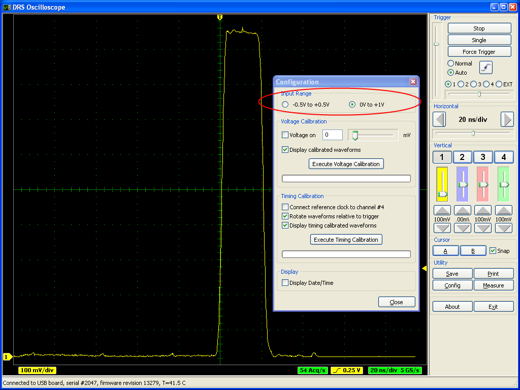
A board firmware update is not necessary for this. It was originally planned to have even a negative range -1V...0V, but this is not possible with the current board design. People who want to record negative pulses have to use an inverter to produce positive pulses. In a future version of the board it might be possible to include this functionality since this is determined by the analog front-end and not the DRS4 chip. |
|
Tue Sep 5 03:28:52 2023, Matias Henriquez, Input range switch added in Version 2.1.3
|
Hello,
It is not quite clear to me yet how the input range is only determined by the front end and not the DRS4 chip. According to the datasheet, the selection of ROFS determines whether the input differential range is -0.5V to 0.5V (ROFS=1.55V) or 0V to 1V (ROFS=1.05V) or -0.05V to 0.95V (ROFS=1.1V).
As far as I understand, the input differential voltage cannot go further below -0.55V since the maximum ROFS voltage is 1.6V according to the datasheet).
Also in the DRS4 evaluation board 5.1 design, the output of the differential amplifier is AC coupled to the DRS4 chip.
I'd appreciate a lot your help.
Regards,
Matias
| Stefan Ritt wrote: |
|
A new software verison for the DRS4 Evaluation Board has been has been released. Version 2.1.3 adds a switch for the input range of the DRS4 board. Once can choose between -0.5V...0.5V and 0V...1V:
A board firmware update is not necessary for this. It was originally planned to have even a negative range -1V...0V, but this is not possible with the current board design. People who want to record negative pulses have to use an inverter to produce positive pulses. In a future version of the board it might be possible to include this functionality since this is determined by the analog front-end and not the DRS4 chip.
|
|
|
Wed Sep 13 13:18:45 2023, Stefan Ritt, Input range switch added in Version 2.1.3
|
To achieve an input range of -1V to 0V, you need an external buffer which can shift this range into the DRS4 range of -0.5V to +0.5V. This external buffer has then to operate with bipolar power supplies, like -2.5V to +2.5V, which are not present on the evaluation board.
Best regards,
Stefan |
|
Fri Jun 9 04:11:40 2023, Javier Caravaca, Different sampling rates in multi-board configuration
|
Hello,
Is it possible to have different sampling rates in multi-board configuration? I tried using the scope application but I am unable to change the sampling rate independently.
Best,
Javier. |
|
Mon Jun 12 14:22:04 2023, Stefan Ritt, Different sampling rates in multi-board configuration
|
No, that's unfortunately not possible.
Stefan
| Javier Caravaca wrote: |
|
Hello,
Is it possible to have different sampling rates in multi-board configuration? I tried using the scope application but I am unable to change the sampling rate independently.
Best,
Javier.
|
|
|
Mon Oct 17 16:29:37 2022, Sebastian Infante, DRS4 installation via tar in ubuntu not working
|
Hello i cant install any the last versions that i downloaded from the dropbox, i can untar the file called drs-5.0.6 and when i type "make" while inside the extracted folder that starts working properly till a point and i get an error, its worth mention that i installed wxWidgets and could make a simple hello world that worked properly in wxWidgets.
The error that i get is the next one:
inlined from ‘bool ResponseCalibration::ReadCalibrationV4(unsigned int)’ at src/DRS.cpp:7224:35:
/usr/include/x86_64-linux-gnu/bits/string_fortified.h:95:34: warning: ‘char* __builtin___strncpy_chk(char*, const char*, long unsigned int, long unsigned int)’ specified bound depends on the length of the source argument [-Wstringop-truncation]
95 | return __builtin___strncpy_chk (__dest, __src, __len,
| ~~~~~~~~~~~~~~~~~~~~~~~~^~~~~~~~~~~~~~~~~~~~~~
96 | __glibc_objsize (__dest));
| ~~~~~~~~~~~~~~~~~~~~~~~~~
src/DRS.cpp: In member function ‘bool ResponseCalibration::ReadCalibrationV4(unsigned int)’:
src/DRS.cpp:4767:11: note: length computed here
4767 | strncpy(calibrationDirectoryPath, fCalibDirectory, strlen(fCalibDirectory));
| ~~~~~~~^~~~~~~~~~~~~~~~~~~~~~~~~~~~~~~~~~~~~~~~~~~~~~~~~~~~~~~~~~~~~~~~~~~~
In file included from /usr/include/string.h:535,
from /usr/local/include/wx-3.3/wx/string.h:30,
from /usr/local/include/wx-3.3/wx/memory.h:15,
from /usr/local/include/wx-3.3/wx/object.h:19,
from /usr/local/include/wx-3.3/wx/wx.h:15,
from src/DRS.cpp:15:
In function ‘char* strncpy(char*, const char*, size_t)’,
inlined from ‘void DRSBoard::GetCalibrationDirectory(char*)’ at src/DRS.cpp:4767:11,
inlined from ‘bool ResponseCalibration::ReadCalibrationV3(unsigned int)’ at src/DRS.cpp:7066:35:
/usr/include/x86_64-linux-gnu/bits/string_fortified.h:95:34: warning: ‘char* __builtin___strncpy_chk(char*, const char*, long unsigned int, long unsigned int)’ specified bound depends on the length of the source argument [-Wstringop-truncation]
95 | return __builtin___strncpy_chk (__dest, __src, __len,
| ~~~~~~~~~~~~~~~~~~~~~~~~^~~~~~~~~~~~~~~~~~~~~~
96 | __glibc_objsize (__dest));
| ~~~~~~~~~~~~~~~~~~~~~~~~~
src/DRS.cpp: In member function ‘bool ResponseCalibration::ReadCalibrationV3(unsigned int)’:
src/DRS.cpp:4767:11: note: length computed here
4767 | strncpy(calibrationDirectoryPath, fCalibDirectory, strlen(fCalibDirectory));
| ~~~~~~~^~~~~~~~~~~~~~~~~~~~~~~~~~~~~~~~~~~~~~~~~~~~~~~~~~~~~~~~~~~~~~~~~~~~
g++ -g -O2 -Wall -Wuninitialized -fno-strict-aliasing -Iinclude -I/usr/local/include -DOS_LINUX -DHAVE_USB -DHAVE_LIBUSB10 -DUSE_DRS_MUTEX -I/usr/local/lib/wx/include/gtk3-unicode-3.3 -I/usr/local/include/wx-3.3 -D_FILE_OFFSET_BITS=64 -DWXUSINGDLL -D__WXGTK__ -pthread -c src/averager.cpp
g++ -g -O2 -Wall -Wuninitialized -fno-strict-aliasing -Iinclude -I/usr/local/include -DOS_LINUX -DHAVE_USB -DHAVE_LIBUSB10 -DUSE_DRS_MUTEX -I/usr/local/lib/wx/include/gtk3-unicode-3.3 -I/usr/local/include/wx-3.3 -D_FILE_OFFSET_BITS=64 -DWXUSINGDLL -D__WXGTK__ -pthread -c src/ConfigDialog.cpp
In file included from include/DRSOscInc.h:25,
from src/ConfigDialog.cpp:7:
include/DOFrame.h: In member function ‘bool DOFrame::GetRefclk()’:
include/DOFrame.h:111:46: error: ordered comparison of pointer with integer zero (‘bool*’ and ‘int’)
111 | bool GetRefclk() { return m_refClk > 0; }
| ~~~~~~~~~^~~
make: *** [Makefile:81: ConfigDialog.o] Error 1
|
|
Mon Feb 6 13:28:28 2023, Stefan Ritt, DRS4 installation via tar in ubuntu not working
|
I fixed the described error. Can you try the new version from https://bitbucket.org/ritt/drs4eb/commits/80b3af753ed32eb365725f0f3244a4109347c01b
| Sebastian Infante wrote: |
|
Hello i cant install any the last versions that i downloaded from the dropbox, i can untar the file called drs-5.0.6 and when i type "make" while inside the extracted folder that starts working properly till a point and i get an error, its worth mention that i installed wxWidgets and could make a simple hello world that worked properly in wxWidgets.
The error that i get is the next one:
inlined from ‘bool ResponseCalibration::ReadCalibrationV4(unsigned int)’ at src/DRS.cpp:7224:35:
/usr/include/x86_64-linux-gnu/bits/string_fortified.h:95:34: warning: ‘char* __builtin___strncpy_chk(char*, const char*, long unsigned int, long unsigned int)’ specified bound depends on the length of the source argument [-Wstringop-truncation]
95 | return __builtin___strncpy_chk (__dest, __src, __len,
| ~~~~~~~~~~~~~~~~~~~~~~~~^~~~~~~~~~~~~~~~~~~~~~
96 | __glibc_objsize (__dest));
| ~~~~~~~~~~~~~~~~~~~~~~~~~
src/DRS.cpp: In member function ‘bool ResponseCalibration::ReadCalibrationV4(unsigned int)’:
src/DRS.cpp:4767:11: note: length computed here
4767 | strncpy(calibrationDirectoryPath, fCalibDirectory, strlen(fCalibDirectory));
| ~~~~~~~^~~~~~~~~~~~~~~~~~~~~~~~~~~~~~~~~~~~~~~~~~~~~~~~~~~~~~~~~~~~~~~~~~~~
In file included from /usr/include/string.h:535,
from /usr/local/include/wx-3.3/wx/string.h:30,
from /usr/local/include/wx-3.3/wx/memory.h:15,
from /usr/local/include/wx-3.3/wx/object.h:19,
from /usr/local/include/wx-3.3/wx/wx.h:15,
from src/DRS.cpp:15:
In function ‘char* strncpy(char*, const char*, size_t)’,
inlined from ‘void DRSBoard::GetCalibrationDirectory(char*)’ at src/DRS.cpp:4767:11,
inlined from ‘bool ResponseCalibration::ReadCalibrationV3(unsigned int)’ at src/DRS.cpp:7066:35:
/usr/include/x86_64-linux-gnu/bits/string_fortified.h:95:34: warning: ‘char* __builtin___strncpy_chk(char*, const char*, long unsigned int, long unsigned int)’ specified bound depends on the length of the source argument [-Wstringop-truncation]
95 | return __builtin___strncpy_chk (__dest, __src, __len,
| ~~~~~~~~~~~~~~~~~~~~~~~~^~~~~~~~~~~~~~~~~~~~~~
96 | __glibc_objsize (__dest));
| ~~~~~~~~~~~~~~~~~~~~~~~~~
src/DRS.cpp: In member function ‘bool ResponseCalibration::ReadCalibrationV3(unsigned int)’:
src/DRS.cpp:4767:11: note: length computed here
4767 | strncpy(calibrationDirectoryPath, fCalibDirectory, strlen(fCalibDirectory));
| ~~~~~~~^~~~~~~~~~~~~~~~~~~~~~~~~~~~~~~~~~~~~~~~~~~~~~~~~~~~~~~~~~~~~~~~~~~~
g++ -g -O2 -Wall -Wuninitialized -fno-strict-aliasing -Iinclude -I/usr/local/include -DOS_LINUX -DHAVE_USB -DHAVE_LIBUSB10 -DUSE_DRS_MUTEX -I/usr/local/lib/wx/include/gtk3-unicode-3.3 -I/usr/local/include/wx-3.3 -D_FILE_OFFSET_BITS=64 -DWXUSINGDLL -D__WXGTK__ -pthread -c src/averager.cpp
g++ -g -O2 -Wall -Wuninitialized -fno-strict-aliasing -Iinclude -I/usr/local/include -DOS_LINUX -DHAVE_USB -DHAVE_LIBUSB10 -DUSE_DRS_MUTEX -I/usr/local/lib/wx/include/gtk3-unicode-3.3 -I/usr/local/include/wx-3.3 -D_FILE_OFFSET_BITS=64 -DWXUSINGDLL -D__WXGTK__ -pthread -c src/ConfigDialog.cpp
In file included from include/DRSOscInc.h:25,
from src/ConfigDialog.cpp:7:
include/DOFrame.h: In member function ‘bool DOFrame::GetRefclk()’:
include/DOFrame.h:111:46: error: ordered comparison of pointer with integer zero (‘bool*’ and ‘int’)
111 | bool GetRefclk() { return m_refClk > 0; }
| ~~~~~~~~~^~~
make: *** [Makefile:81: ConfigDialog.o] Error 1
|
|
|
Sat Oct 22 13:24:20 2022, Phan Van Chuan, Channel Cascading Option in the 2048-bin
|
Dear Stefan,
We are using DRS4 evaluation board version 5.1 and firmware version 30000 (as the picture attached). Now, I am in need one channel with length 2048 bin. However, I can't find the resistors R99, ... ,R106 on the hardware of evaluation board; it seems my DRS4 evaluation board doesn't use 2048 bins per channel.
Our question is, can we repair this hardware to read 2048 bins/channel? if that is possible please let me know what to add on hardware/software of DRS4 evaluation.
Best regards.
Phan Van Chuan. |
|
Mon Oct 24 12:50:24 2022, Stefan Ritt, Channel Cascading Option in the 2048-bin
|
The board is delivered in one or the other mode and not meant to be changed by the user, since this requires very delicate soldering which is not easy. If you try anyhow, you loose the quarantee. You can send the board back to the manufacturer for the modification, but this costs quite some moeny.
Best regards,
Stefan
| Phan Van Chuan wrote: |
|
Dear Stefan,
We are using DRS4 evaluation board version 5.1 and firmware version 30000 (as the picture attached). Now, I am in need one channel with length 2048 bin. However, I can't find the resistors R99, ... ,R106 on the hardware of evaluation board; it seems my DRS4 evaluation board doesn't use 2048 bins per channel.
Our question is, can we repair this hardware to read 2048 bins/channel? if that is possible please let me know what to add on hardware/software of DRS4 evaluation.
Best regards.
Phan Van Chuan.
|
|
|
Tue Sep 27 10:17:58 2022, Kunal Shinde, Required Firmware for DRS4 Evaluation Board Version 2.0
|
Hi, I am working on an old DRS4 board Version "2.0" with firmware revision "13191", I was unable to find this specific firmware source files ("VHDL source code"), please help me where could I find this or send me the required.
Regards,
Kunal |
|
Tue Sep 27 10:37:11 2022, Stefan Ritt, Required Firmware for DRS4 Evaluation Board Version 2.0
|
You find each software version at the usual download location at
https://www.dropbox.com/home/drs/drs4/distribution/Download/Linux
The one you need is probably drs-2.1.3.tar.gz which was the last version for the 2.0 board which is now more than 10 years old.
Best,
Stefan
| Kunal Shinde wrote: |
|
Hi, I am working on an old DRS4 board Version "2.0" with firmware revision "13191", I was unable to find this specific firmware source files ("VHDL source code"), please help me where could I find this or send me the required.
Regards,
Kunal
|
|
|
Tue Sep 27 10:52:41 2022, Kunal Shinde, Required Firmware for DRS4 Evaluation Board Version 2.0
|
I checked the link you provided but it seems that the link doesnt exist please send me valid one.
Regards,
Kunal
| Stefan Ritt wrote: |
|
You find each software version at the usual download location at
https://www.dropbox.com/home/drs/drs4/distribution/Download/Linux
The one you need is probably drs-2.1.3.tar.gz which was the last version for the 2.0 board which is now more than 10 years old.
Best,
Stefan
| Kunal Shinde wrote: |
|
Hi, I am working on an old DRS4 board Version "2.0" with firmware revision "13191", I was unable to find this specific firmware source files ("VHDL source code"), please help me where could I find this or send me the required.
Regards,
Kunal
|
|
|
|
Tue Sep 27 15:20:55 2022, Stefan Ritt, Required Firmware for DRS4 Evaluation Board Version 2.0
|
Sorry, got the wrong link. Here the right one: https://www.dropbox.com/sh/clqo7ekr0ysbrip/AACoWJzrQAbf3WiBJHG89bGGa?dl=0
If you untar the archive, you will find a "firmware" subdirectory with all VHDL code.
Stefan
| Kunal Shinde wrote: |
|
I checked the link you provided but it seems that the link doesnt exist please send me valid one.
Regards,
Kunal
| Stefan Ritt wrote: |
|
You find each software version at the usual download location at
https://www.dropbox.com/home/drs/drs4/distribution/Download/Linux
The one you need is probably drs-2.1.3.tar.gz which was the last version for the 2.0 board which is now more than 10 years old.
Best,
Stefan
| Kunal Shinde wrote: |
|
Hi, I am working on an old DRS4 board Version "2.0" with firmware revision "13191", I was unable to find this specific firmware source files ("VHDL source code"), please help me where could I find this or send me the required.
Regards,
Kunal
|
|
|
|
|