| ID |
Date |
Author |
Subject |
|
823
|
Fri Apr 9 20:29:45 2021 |
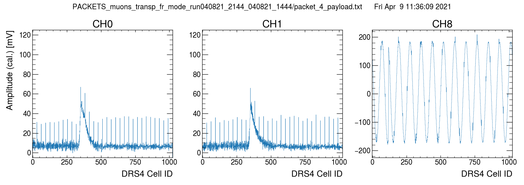
Sean Quinn | Spikes/noise sensitive to clock settings? | Dear DRS4 team,
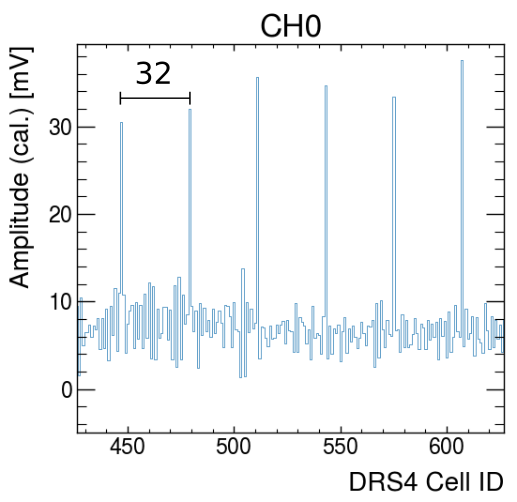
I'm trying to troubleshoot some odd spike behavior. If I run the ADC and SR CLK at 16 MHz (behavior also seen at 33 MHz) we get very noisy data (post-calibration) with periodic spikes.
In the below plot
- CH0 & CH1 are muon pulses from a scintillator + SiPM detector
- CH8 is a 25 MHz sinewave (in phase with all generated board clocks)
- Transparent mode = ON
- ROI = OFF, "full readout mode", first sample = cell 0
- DRS REFCLK = 1 MHz (2 GS/s)
- ADC & SR CLK = 16 MHz, 0 deg. offset
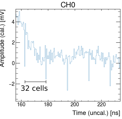
After I modify some clock settings, things seem to improve dramatically, and the spike behavior changes
- ADC and SR CLK = 15 MHz, 0 deg. offset
- Transparent mode = ON
- ROI = ON (just for testing purposes)
- Add 1.064 ns skew to DRS REF CLK
- NOTE: Unfortunately due to a design mishap, the ADC and FPGA clock use a phase-locked output pair on our clock synthesis chip, so we cannot fine-tune the skew for it.
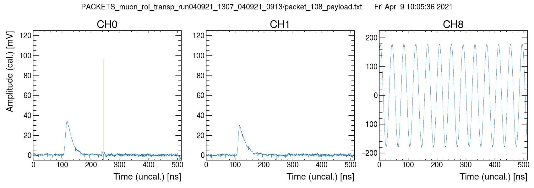
Observed differences
- Spike polarity seems inverted
- Spikes limited to smaller number of cells now?
- Spike amplitude reduced
- Overall baseline variance seems better
- New large positive spike artifact on CH0 that seems inverted on CH1
- CH8 seems unaffected by large spikes?
Artifacts seem related to clock configuration, but I am sort of in the dark on what might be happening from a first-principles point of view. Any tips?
Warm regards,
Sean |
|
825
|
Fri Apr 9 21:38:59 2021 |
Stefan Ritt | Spikes/noise sensitive to clock settings? | elog:824
| Sean Quinn wrote: |
|
Dear DRS4 team,
I'm trying to troubleshoot some odd spike behavior. If I run the ADC and SR CLK at 16 MHz (behavior also seen at 33 MHz) we get very noisy data (post-calibration) with periodic spikes.
In the below plot
- CH0 & CH1 are muon pulses from a scintillator + SiPM detector
- CH8 is a 25 MHz sinewave (in phase with all generated board clocks)
- Transparent mode = ON
- ROI = OFF, "full readout mode", first sample = cell 0
- DRS REFCLK = 1 MHz (2 GS/s)
- ADC & SR CLK = 16 MHz, 0 deg. offset
After I modify some clock settings, things seem to improve dramatically, and the spike behavior changes
- ADC and SR CLK = 15 MHz, 0 deg. offset
- Transparent mode = ON
- ROI = ON (just for testing purposes)
- Add 1.064 ns skew to DRS REF CLK
- NOTE: Unfortunately due to a design mishap, the ADC and FPGA clock use a phase-locked output pair on our clock synthesis chip, so we cannot fine-tune the skew for it.
Observed differences
- Spike polarity seems inverted
- Spikes limited to smaller number of cells now?
- Spike amplitude reduced
- Overall baseline variance seems better
- New large positive spike artifact on CH0 that seems inverted on CH1
- CH8 seems unaffected by large spikes?
Artifacts seem related to clock configuration, but I am sort of in the dark on what might be happening from a first-principles point of view. Any tips?
Warm regards,
Sean
|
|
|
885
|
Fri Jun 24 09:57:36 2022 |
LynseyShun | Spikes/noise sensitive to clock settings? | Hello, I now have periodic spikes in CH0 and CH1 output. How can I eliminate these spikes? I'm sorry I didn't understand your elimination method. Please explain the method in detail. Thank you very much
| Stefan Ritt wrote: |
|
elog:824
| Sean Quinn wrote: |
|
Dear DRS4 team,
I'm trying to troubleshoot some odd spike behavior. If I run the ADC and SR CLK at 16 MHz (behavior also seen at 33 MHz) we get very noisy data (post-calibration) with periodic spikes.
In the below plot
- CH0 & CH1 are muon pulses from a scintillator + SiPM detector
- CH8 is a 25 MHz sinewave (in phase with all generated board clocks)
- Transparent mode = ON
- ROI = OFF, "full readout mode", first sample = cell 0
- DRS REFCLK = 1 MHz (2 GS/s)
- ADC & SR CLK = 16 MHz, 0 deg. offset
After I modify some clock settings, things seem to improve dramatically, and the spike behavior changes
- ADC and SR CLK = 15 MHz, 0 deg. offset
- Transparent mode = ON
- ROI = ON (just for testing purposes)
- Add 1.064 ns skew to DRS REF CLK
- NOTE: Unfortunately due to a design mishap, the ADC and FPGA clock use a phase-locked output pair on our clock synthesis chip, so we cannot fine-tune the skew for it.
Observed differences
- Spike polarity seems inverted
- Spikes limited to smaller number of cells now?
- Spike amplitude reduced
- Overall baseline variance seems better
- New large positive spike artifact on CH0 that seems inverted on CH1
- CH8 seems unaffected by large spikes?
Artifacts seem related to clock configuration, but I am sort of in the dark on what might be happening from a first-principles point of view. Any tips?
Warm regards,
Sean
|
|
|
|
888
|
Fri Jul 29 17:23:43 2022 |
Stefan Ritt | Spikes/noise sensitive to clock settings? | Look at the DRS4 data sheet, Figure 12. You see there the rising SRCLK pulse which outputs the next analog value. You also see tSAMP which describes the sampling piont (strobe or clock sent to your ADC). The value of tSAMP must be such that the values is sampled at the point where it flattens out, just 2-3 ns BEFORE the next analog sample is clocked out, as written in the text. So you have to phase shift your clock going to SRCLK and the one going to your ADC against each other. This needs adjustment at the ns level, so you need a PLL with fine-valued taps, so you can shift it in fractions of a ns. What you see is that you sample at the BEGINNING of a new value to be output to the chip. Please also note that most ADCs have an internal delay of their clock (usually called 'aperture') which has to be taken into account. So if your SRCLK and your ADC clock come at the same time (not phase shifted), it might happen that the ADC internal aperture delay caues it to sample the analog signal at the BEGINNING of the new value.
Hope this is clearer now.
Best regards,
Stefan |
|
348
|
Tue May 27 13:46:18 2014 |
Dominik Neise | Spikes in DRS4 data on custom baord. | We see quite some spikes in our DRS4 sampled data in FACT. We see different types of spikes:
- single cell spikes, usually showing a large amplitude of 200mV
- double cell spikes, usually only in the order of 20mV.
- Even triple and quadro cell spikes are rarely seen.
The double cell spikes often occur as symmetrical double cell spikes mirrored at cell 512. quadro cell spikes seem to be nothing else, than connected symmetrical double cell spikes. For the triple cell spikes we have no idea.
Currently we use simple filters to get rid of these spikes, this workes rather well for the large single cell spikes, but with the occurance of tripples and quadros we started to worry about higher multiples and revived our DRS4 spike investigations.
Now I was told, that you Stefan know already where these spikes come from and even a paper exisits. Unfortunately so far I was unable to find it.
I wonder if it is possible to predict the occurance of these spikes, so one does not have to search for them anymore and can get rid of the filters.
Best regards
Dominik |
|
349
|
Tue May 27 16:07:17 2014 |
Stefan Ritt | Spikes in DRS4 data on custom baord. |
| Dominik Neise wrote: |
|
We see quite some spikes in our DRS4 sampled data in FACT. We see different types of spikes:
- single cell spikes, usually showing a large amplitude of 200mV
- double cell spikes, usually only in the order of 20mV.
- Even triple and quadro cell spikes are rarely seen.
The double cell spikes often occur as symmetrical double cell spikes mirrored at cell 512. quadro cell spikes seem to be nothing else, than connected symmetrical double cell spikes. For the triple cell spikes we have no idea.
Currently we use simple filters to get rid of these spikes, this workes rather well for the large single cell spikes, but with the occurance of tripples and quadros we started to worry about higher multiples and revived our DRS4 spike investigations.
Now I was told, that you Stefan know already where these spikes come from and even a paper exisits. Unfortunately so far I was unable to find it.
I wonder if it is possible to predict the occurance of these spikes, so one does not have to search for them anymore and can get rid of the filters.
Best regards
Dominik
|
All I know is that the "20mV" spikes are always symmetrical around cell #512, that they are typically 17.4 mV in height, and that they occur always in all 9 channels simultaneously. They cannot occur in all locations, but there only like 32 possible locations where they can occur. With this information it should be easy to fix them by filtering.
200 mV spikes are new to me. I do not see them in our boards, so it must be related to the board readout and not to the chip.
Best regards,
Stefan
|
|
289
|
Wed Aug 28 13:07:51 2013 |
Andrey Kuznetsov | Some bug fixes and questions | For http://www.psi.ch/drs/DocumentationEN/manual_rev20.pdf:
0 0x02 15..8 board_type 5 for DRS4 USB Evaluation Board 1.1 ---> should instead say Evaluation Board 2.0 ?
I've been reviewing DRS.cpp v4.0.1
1) if(i==100) should be if(i==1000) in function int DRSBoard::SetFrequency(double demand, bool wait)
Otherwise if PLL did not lock, i = 1000, and the if statement is evaluating it against 100, not 1000 so it never gets triggered and the error goes unnoticed.
if (wait) {
StartDomino();
for (i=0 ; i<1000 ; i++)
if (GetStatusReg() & BIT_PLL_LOCKED0)
break;
SoftTrigger();
if (i==100) {
printf("PLL did not lock for frequency %lf\n", demand);
return 0;
}
}
2) int DRSBoard::RegulateFrequency(double demand) does not seem to work at all, the frequency does not lock for either 2 or 5 GHz, tested using DRS4 v2.0 eval board with DRS v4.0.1 and v2.0.1 software's drscl tool.
3) In int DRSBoard::SetTriggerDelayPercent(int delay) and int DRSBoard::SetTriggerDelayNs(int delay), what is the purpose of Read and setting of "reg" if it's not being used or exported anywhere else outside of that function? Seems like Read and reg are called for nothing.
Read(T_CTRL, ®, REG_TRG_DELAY, 2);
reg = (reg & 0xFF00) | ticks;
Write(T_CTRL, REG_TRG_DELAY, &ticks, 2);
Also, I don't understand why in int DRSBoard::SetSyncDelay(int ticks), the code changes to Read(T_CTRL, ®, REG_TRG_DELAY, 2);
reg = (reg & 0xFF) | (ticks << 8);
Write(T_CTRL, REG_TRG_DELAY, ®, 2);
In particular, reg = (reg & 0xFF00) | ticks; and reg = (reg & 0xFF) | (ticks << 8); I'm not really sure but doesn't Read() with size 2 return a value that has a maximum value of 0xFF, or 8bits? But ticks << 8, since ticks == 255 max, makes 255 << 8 => 65280, which is now a 16bit value and size 4. No? I might be wrong here, and if I am then I don't understand what's going on. Can you please explain? In v2.0.1 the ticks were a maximum of 511 or 9bits, why did it change to 8bits?
4) A function is being called incorrectly in GetWave() in DRS.cpp
int DRSBoard::GetWave(unsigned int chipIndex, unsigned char channel, float *waveform)

{
   return GetWave(chipIndex, channel, waveform, true, fStopCell[chipIndex], false, 0, true);

}
The return is calling the following overloaded function:
int DRSBoard::GetWave(unsigned int chipIndex, unsigned char channel, float *waveform, bool responseCalib, int triggerCell, int wsr, bool adjustToClock, float threshold, bool offsetCalib)
the problem is that int wsr is not passed to the function and it thus causes implicit conversions where false is being cast into int, 0 into bool, and true into float.
I'll post more if I have any questions or spot any more bugs. |
|
290
|
Thu Sep 5 10:01:00 2013 |
Andrey Kuznetsov | Some bug fixes and questions | #11 0x080589de in DRSBoard::GetWave (this=0xb7456008, chipIndex=0, channel=0 '\000', waveform=0x40f24000, responseCalib=true, triggerCell=207, wsr=0, adjustToClock=false, threshold=1, offsetCalib=true) at src/DRS.cpp:3380
This is calling:
int GetWave(unsigned int chipIndex, unsigned char channel, float *waveform, bool responseCalib, int triggerCell = -1, int wsr = -1, bool adjustToClock = false, float threshold = 0, bool offsetCalib = true);
from DRS.cpp:
return GetWave(chipIndex, channel, waveform, true, fStopCell[chipIndex], false, 0, true);

false=0
true=1

As you can see offsetCalib ends up being defined by default, threshold set to 1 because of true, adjustToClock is false set by 0, wsr is 0 set by false, however threshold is never used with DRS4 eval board. So although it doesn't affect data retrieval, it's just dumb luck the function ends up being called with parameters that matter being exactly what they were meant to be.
|
|
291
|
Mon Sep 9 06:49:36 2013 |
Andrey Kuznetsov | Some bug fixes and questions | The DRSCallback *pcb is missing an if statement in the code when DRS Oscilloscope software isn't used when calibrating in function: int DRSBoard::CalibrateTiming(DRSCallback *pcb)
I had to add if (pcb != NULL) before each pcb call, like other functions are using so that the program doesn't segfault when the function is called like b->CalibrateTiming(NULL);
That's the only function that's missing this if statement for DRSCallback *pcb call, and there are 2 calls in this function to pcb that need fixing. |
|
325
|
Wed Jan 15 16:15:00 2014 |
Stefan Ritt | Some bug fixes and questions |
Type 5 is both for board V1.1 and V2. I consider V1.1 obsolete (nobody uses it). I added code 8 for V4 and 9 for V5
| Andrey Kuznetsov wrote: |
|
1) if(i==100) should be if(i==1000) in function int DRSBoard::SetFrequency(double demand, bool wait)
Otherwise if PLL did not lock, i = 1000, and the if statement is evaluating it against 100, not 1000 so it never gets triggered and the error goes unnoticed.
if (wait) {
StartDomino();
for (i=0 ; i<1000 ; i++)
if (GetStatusReg() & BIT_PLL_LOCKED0)
break;
SoftTrigger();
if (i==100) {
printf("PLL did not lock for frequency %lf\n", demand);
return 0;
}
}
|
Absolutely correct, I changed it in the current software.
| Andrey Kuznetsov wrote: |
|
2) int DRSBoard::RegulateFrequency(double demand) does not seem to work at all, the frequency does not lock for either 2 or 5 GHz, tested using DRS4 v2.0 eval board with DRS v4.0.1 and v2.0.1 software's drscl tool.
|
This function is for the old DRS2 chip back in 2003 or so. That chip did not have an on-chip PLL for frequency regulation, so this was done in the FPGA. Just don't us it (who told you to???).
| Andrey Kuznetsov wrote: |
|
3) In int DRSBoard::SetTriggerDelayPercent(int delay) and int DRSBoard::SetTriggerDelayNs(int delay), what is the purpose of Read and setting of "reg" if it's not being used or exported anywhere else outside of that function? Seems like Read and reg are called for nothing.
Read(T_CTRL, ®, REG_TRG_DELAY, 2);
reg = (reg & 0xFF00) | ticks;
Write(T_CTRL, REG_TRG_DELAY, &ticks, 2);
Also, I don't understand why in int DRSBoard::SetSyncDelay(int ticks), the code changes to Read(T_CTRL, ®, REG_TRG_DELAY, 2);
reg = (reg & 0xFF) | (ticks << 8);
Write(T_CTRL, REG_TRG_DELAY, ®, 2);
In particular, reg = (reg & 0xFF00) | ticks; and reg = (reg & 0xFF) | (ticks << 8); I'm not really sure but doesn't Read() with size 2 return a value that has a maximum value of 0xFF, or 8bits? But ticks << 8, since ticks == 255 max, makes 255 << 8 => 65280, which is now a 16bit value and size 4. No? I might be wrong here, and if I am then I don't understand what's going on. Can you please explain? In v2.0.1 the ticks were a maximum of 511 or 9bits, why did it change to 8bits?
|
The register REG_TRG_DELAY contains two 8-bit values, one for the trigger delay, one for the sync delay (which is currently not used). So to set one half of the register containing 16 bits, the register is read (16 bits are read with size 2, since these are two bytes), and the upper or lower 8 bits are replaced with the new value. Then the 16 bits are written back. The firmware in the FPGA does not allow to access only 8 bits of a 16-bit register.
| Andrey Kuznetsov wrote: |
|
4) A function is being called incorrectly in GetWave() in DRS.cpp
int DRSBoard::GetWave(unsigned int chipIndex, unsigned char channel, float *waveform)

{
               return GetWave(chipIndex, channel, waveform, true, fStopCell[chipIndex], false, 0, true);

}
The return is calling the following overloaded function:
int DRSBoard::GetWave(unsigned int chipIndex, unsigned char channel, float *waveform, bool responseCalib, int triggerCell, int wsr, bool adjustToClock, float threshold, bool offsetCalib)
            the problem is that int wsr is not passed to the function and it thus causes implicit conversions where false is being cast into int, 0 into bool, and true into float.
|
That's correct. Fortunately the wrong values for the wsr does not have any influence for "normal" users. It is only used for channel cascading which is not used in the evaluation board. I will fix it in the code anyhow. |
|
326
|
Wed Jan 15 17:02:58 2014 |
Stefan Ritt | Some bug fixes and questions |
| Andrey Kuznetsov wrote: |
|
So although it doesn't affect data retrieval, it's just dumb luck the function ends up being called with parameters that matter being exactly what they were meant to be.
|
Exactly. If I would not have had that dumb luck, I would have seen the problem and fixed it. So it was more like bad luck. |
|
327
|
Wed Jan 15 17:11:14 2014 |
Stefan Ritt | Some bug fixes and questions |
| Andrey Kuznetsov wrote: |
|
The DRSCallback *pcb is missing an if statement in the code when DRS Oscilloscope software isn't used when calibrating in function: int DRSBoard::CalibrateTiming(DRSCallback *pcb)
I had to add if (pcb != NULL) before each pcb call, like other functions are using so that the program doesn't segfault when the function is called like b->CalibrateTiming(NULL);
That's the only function that's missing this if statement for DRSCallback *pcb call, and there are 2 calls in this function to pcb that need fixing.
|
Acknowledged. Added it to the code. |
|
332
|
Wed Mar 5 21:54:13 2014 |
Hermann-Josef Mathes | Software drs-5.0.0 fails to compile (drsosc) | Hi,
the latest software drs-5.0.0.tar.gz fails to compile on my freshly installed SuSE 13.1 whereas the previous 4.0.1 is compiling out-of-the-box.
My system has the wxWidgets 2.8.12 which is probably together with gcc 4.8.1 the reason of the problem. I applied a number of corrections, mainly some sort of proper (?) typecasts, a patch file is attached.
Maybe you could consider to take them into account for the next patch release?
Thanks and best regards
Hermann-Josef
|
| Attachment 1: drs-5.patch
|
diff --git a/src/DOScreen.cpp b/src/DOScreen.cpp
index 0147c29..3f6b665 100644
--- a/src/DOScreen.cpp
+++ b/src/DOScreen.cpp
@@ -110,7 +110,7 @@ void DOScreen::OnPaint(wxPaintEvent& event)

    // Change "Save" button
    if (!m_frame->GetWFfd() && !m_frame->GetWFFile())
-      m_frame->SetSaveBtn("Save", "Save waveforms");
+      m_frame->SetSaveBtn(wxT("Save"), wxT("Save waveforms"));
 }

 /*------------------------------------------------------------------*/
@@ -347,7 +347,7 @@ void DOScreen::DrawScopeBottom(wxDC& dc, int board, int x1, int y1, int width, b
    }
    x_start = x_start - 15 - w;
    if (m_frame->GetNSaved()) {
-      wxst.Printf("%d saved", m_frame->GetNSaved());
+      wxst.Printf(wxT("%d saved"), m_frame->GetNSaved());
       dc.GetTextExtent(wxst, &w, &h);
       dc.DrawRoundedRectangle(x_start-20-w, y1+3, w+10, 15, 2);
       dc.DrawText(wxst, x_start-15-w, y1+3);
diff --git a/src/TriggerDialog.cpp b/src/TriggerDialog.cpp
index 7aeb33e..32b41fa 100644
--- a/src/TriggerDialog.cpp
+++ b/src/TriggerDialog.cpp
@@ -26,13 +26,13 @@ TriggerDialog_fb( parent )
    m_cbANDEXT->SetValue((tc & (1<<12))>0);

    wxString s;
-   s.Printf("%1.3lf", m_frame->GetTrgLevel(0));
+   s.Printf(wxT("%1.3lf"), m_frame->GetTrgLevel(0));
    m_tbLevel1->SetValue(s);
-   s.Printf("%1.3lf", m_frame->GetTrgLevel(1));
+   s.Printf(wxT("%1.3lf"), m_frame->GetTrgLevel(1));
    m_tbLevel2->SetValue(s);
-   s.Printf("%1.3lf", m_frame->GetTrgLevel(2));
+   s.Printf(wxT("%1.3lf"), m_frame->GetTrgLevel(2));
    m_tbLevel3->SetValue(s);
-   s.Printf("%1.3lf", m_frame->GetTrgLevel(3));
+   s.Printf(wxT("%1.3lf"), m_frame->GetTrgLevel(3));
    m_tbLevel4->SetValue(s);
 }

@@ -49,19 +49,19 @@ void TriggerDialog::OnButton( wxCommandEvent& event )
 void TriggerDialog::OnTriggerLevel( wxCommandEvent& event )
 {
    if (event.GetId() == ID_LEVEL1)
-      m_frame->SetTrgLevel(0, atof(m_tbLevel1->GetValue()));
+      m_frame->SetTrgLevel(0, atof(m_tbLevel1->GetValue().mb_str()));
    if (event.GetId() == ID_LEVEL2)
-      m_frame->SetTrgLevel(1, atof(m_tbLevel2->GetValue()));
+      m_frame->SetTrgLevel(1, atof(m_tbLevel2->GetValue().mb_str()));
    if (event.GetId() == ID_LEVEL3)
-      m_frame->SetTrgLevel(2, atof(m_tbLevel3->GetValue()));
+      m_frame->SetTrgLevel(2, atof(m_tbLevel3->GetValue().mb_str()));
    if (event.GetId() == ID_LEVEL4)
-      m_frame->SetTrgLevel(3, atof(m_tbLevel4->GetValue()));
+      m_frame->SetTrgLevel(3, atof(m_tbLevel4->GetValue().mb_str()));
 }

 void TriggerDialog::SetTriggerLevel(double level)
 {
    wxString s;
-   s.Printf("%1.3lf", level);
+   s.Printf(wxT("%1.3lf"), level);
    m_tbLevel1->SetValue(s);
    m_tbLevel2->SetValue(s);
    m_tbLevel3->SetValue(s);
|
|
333
|
Thu Mar 6 11:12:44 2014 |
Stefan Ritt | Software drs-5.0.0 fails to compile (drsosc) |
| Hermann-Josef Mathes wrote: |
|
Hi,
the latest software drs-5.0.0.tar.gz fails to compile on my freshly installed SuSE 13.1 whereas the previous 4.0.1 is compiling out-of-the-box.
My system has the wxWidgets 2.8.12 which is probably together with gcc 4.8.1 the reason of the problem. I applied a number of corrections, mainly some sort of proper (?) typecasts, a patch file is attached.
Maybe you could consider to take them into account for the next patch release?
Thanks and best regards
Hermann-Josef
|
Thank you very much for the corrections. I know it in principle, but neither my Mac OSX nor the Windows compiler complains, so I usually don't see this errors. It's fixed now.
/Stefan |
|
865
|
Wed Feb 16 14:06:45 2022 |
Dmitry Hits | Sliders missing in drsosc | Hi everyone,
Did anyone have a "missing sliders problem" in GUI (see attachment) accompanied by the following message in the terminal.
(drsosc:4611): Gtk-WARNING **: 14:05:11.249: Negative content width -4 (allocation 20, extents 12x12) while allocating gadget (node scale, owner GtkScale)
(drsosc:4611): Gtk-WARNING **: 14:05:11.249: Negative content width -2 (allocation 0, extents 1x1) while allocating gadget (node trough, owner GtkScale)
If yes, how did you solve it?
All ideas are appreciated!
Cheers,
Dmitry
|
| Attachment 1: Screen_Shot_2022-02-14_at_14.17.30.png
|

|
|
906
|
Thu Feb 22 01:21:11 2024 |
Rod McInnis | Simulation of FPGA | Hello:
A bit of background: I am working on a project that is utilizing the DRS4 Evaluation board as a prototype platform for a dedicated, special use capture. We will only be utilizing one channel of the ADC capture, and the 1024 samples is more than enough.
What I will need to do, however, is do some preprocessing on the incoming ADC data, running some calculation on the fly, possibly some filtering and other transformations before putting the data into the FPGA block memory for transfer to the host via the Cypress USB interface. I will be modifying the "drs4_eval5" VHDL file and doing a new FPGA build.
It will be essential that I be able to simulate this, from the ADC input to the data flow to the Cypress chip. I have "eval board files" which includes the VHDL source files, Xilinxe ISE project files and some very basic simulation testbenches.
Unfortunately, the simulation testbenches call out a "drs4_eval1" module while the Xilinx project uses a "drs4_eval5" module, and the module ports are a little different. I think I can work around that, however. I have run the simulatilon "drs4_eval1_tb", which does a simple write to a Control Register. I need to expand this simulation so that it will initiate a full capture and then transfer the data from the RAM to the Cypress chip.
What I am most confused about is how the Cypress chip sucks out the data from the FPGA block ram. I would expect it to use a burst mode data transfer rather than the cumbersom CSR read/write, but I haven't found any documentation on how this interface works.
Q1: Is there a simulation testbench file available that does the 1024 sample data transfer?
Q2: Is there a waveform diagram that shows the protocol / signal handshake between the FPGA and Cypress chip for this data transfer?
Thank you
Rod McInnis
|
|
907
|
Thu Feb 22 10:37:03 2024 |
Stefan Ritt | Simulation of FPGA | The Cypress has its own firmware, contained in the distribution under firmware/CY7C68013A/drs_eval.c. There you can see how the data is fetched. I kind of forgot how exactly it worked, since I wrote that code back in 2011. But most if the Cypress code is just the configuration of the USB, the communication with the FPGA is kind of straight forward in the Cypress implementation. But you have to read the manual of that chip to understand it.
Unfrtunately there is no full testbench for the firmware, since I didn't have a VHDL Model of the Cypress, so I implemente dit the "hard" way ;-)
Best,
Stefan
| Rod McInnis wrote: |
|
Hello:
A bit of background: I am working on a project that is utilizing the DRS4 Evaluation board as a prototype platform for a dedicated, special use capture. We will only be utilizing one channel of the ADC capture, and the 1024 samples is more than enough.
What I will need to do, however, is do some preprocessing on the incoming ADC data, running some calculation on the fly, possibly some filtering and other transformations before putting the data into the FPGA block memory for transfer to the host via the Cypress USB interface. I will be modifying the "drs4_eval5" VHDL file and doing a new FPGA build.
It will be essential that I be able to simulate this, from the ADC input to the data flow to the Cypress chip. I have "eval board files" which includes the VHDL source files, Xilinxe ISE project files and some very basic simulation testbenches.
Unfortunately, the simulation testbenches call out a "drs4_eval1" module while the Xilinx project uses a "drs4_eval5" module, and the module ports are a little different. I think I can work around that, however. I have run the simulatilon "drs4_eval1_tb", which does a simple write to a Control Register. I need to expand this simulation so that it will initiate a full capture and then transfer the data from the RAM to the Cypress chip.
What I am most confused about is how the Cypress chip sucks out the data from the FPGA block ram. I would expect it to use a burst mode data transfer rather than the cumbersom CSR read/write, but I haven't found any documentation on how this interface works.
Q1: Is there a simulation testbench file available that does the 1024 sample data transfer?
Q2: Is there a waveform diagram that shows the protocol / signal handshake between the FPGA and Cypress chip for this data transfer?
Thank you
Rod McInnis
|
|
|
7
|
Tue Apr 28 11:44:07 2009 |
Stefan Ritt | Simple example application to read a DRS evaluation board | Several people asked for s simple application to guide them in writing their own application to read out a DRS board. Such an application has been added in software revions 2.1.1 and is attached to this message. This example program drs_exam.cpp written in C++ does the following necessary steps to access a DRS board:
- Crate a "DRS" object and scan all USB devices
- Display found DRS boards
- Initialize the first found board and set the sampling frequency to 5 GSPS
- Enable internal trigger on channel #1 with 250 mV threshold
- Start acquisition and wait for a trigger
- Read two waveforms (both time and amplitude)
- Repeat this 10 times
I know that we are still missing a good documentation for the DRS API, but I have not yet found the time to do that. I hope the example program is enough for most people to start writing own programs. For Windows users (MS Visual C++ 8.0) there is a drs.sln project file, and for linux users there is a Makefile which can be used to compile this example program.
|
| Attachment 1: drs_exam.cpp
|
/********************************************************************\

  Name:         drs_exam.cpp
  Created by:   Stefan Ritt

  Contents:     Simple example application to read out a DRS4
                evaluation board

  $Id: drs_exam.cpp 13344 2009-04-28 07:34:45Z ritt@PSI.CH $

\********************************************************************/

#include <math.h>

#ifdef _MSC_VER

#include <windows.h>

#elif defined(OS_LINUX)

#define O_BINARY 0

#include <unistd.h>
#include <ctype.h>
#include <sys/ioctl.h>
#include <errno.h>

#define DIR_SEPARATOR '/'

#endif

#include <stdio.h>
#include <string.h>
#include <stdlib.h>

#include "strlcpy.h"
#include "DRS.h"

/*------------------------------------------------------------------*/

int main()
{
   int i, j, nBoards;
   DRS *drs;
   DRSBoard *b;
   float time_array[1024];
   float wave_array[8][1024];

   /* do initial scan */
   drs = new DRS();

   /* show any found board(s) */
   for (i=0 ; i<drs->GetNumberOfBoards() ; i++) {
      b = drs->GetBoard(i);
      printf("Found DRS4 evaluation board, serial #%d, firmware revision %d\n",
         b->GetBoardSerialNumber(), b->GetFirmwareVersion());
   }

   /* exit if no board found */
   nBoards = drs->GetNumberOfBoards();
   if (nBoards == 0) {
      printf("No DRS4 evaluation board found\n");
      return 0;
   }

   /* continue working with first board only */
   b = drs->GetBoard(0);

   /* initialize board */
   b->Init();

   /* set sampling frequency */
   b->SetFrequency(5);

   /* enable transparent mode needed for analog trigger */
   b->SetTranspMode(1);

   /* use following line to disable hardware trigger */
   //b->EnableTrigger(0, 0);

   /* use following line to enable external hardware trigger (Lemo) */
   //b->EnableTrigger(1, 0);

   /* use following lines to enable hardware trigger on CH1 at 250 mV positive edge */
   b->EnableTrigger(0, 1);              // lemo off, analog trigger on
   b->SetTriggerSource(0);              // use CH1 as source
   b->SetTriggerLevel(0.25, false, 0);  // 0.25 V, positive edge, zero delay

   /* repeat ten times */
   for (j=0 ; j<10 ; j++) {

      /* start board (activate domino wave) */
      b->StartDomino();

      /* wait for trigger */
      printf("Waiting for trigger...");
      while (b->IsBusy());

      /* read all waveforms */
      b->TransferWaves(0, 8);

      /* read time (X) array in ns */
      b->GetTime(0, time_array);

      /* decode waveform (Y) array first channel in mV */
      b->GetWave(0, 0, wave_array[0]);

      /* decode waveform (Y) array second channel in mV*/
      b->GetWave(0, 1, wave_array[1]);

      /* process waveform: add here some code to display or save waveform X=time[i], Y=wave_array[n][i] */

      /* print some progress indication */
      printf("\rEvent #%d read successfully\n", j);
   }

   /* delete DRS object -> close USB connection */
   delete drs;
}
|
|
8
|
Wed Apr 29 07:57:33 2009 |
Stefan Ritt | Simple example application to read a DRS evaluation board |
| Stefan Ritt wrote: |
|
Several people asked for s simple application to guide them in writing their own application to read out a DRS board. Such an application has been added in software revions 2.1.1 and is attached to this message. This example program drs_exam.cpp written in C++ does the following necessary steps to access a DRS board:
- Crate a "DRS" object and scan all USB devices
- Display found DRS boards
- Initialize the first found board and set the sampling frequency to 5 GSPS
- Enable internal trigger on channel #1 with 250 mV threshold
- Start acquisition and wait for a trigger
- Read two waveforms (both time and amplitude)
- Repeat this 10 times
I know that we are still missing a good documentation for the DRS API, but I have not yet found the time to do that. I hope the example program is enough for most people to start writing own programs. For Windows users (MS Visual C++ 8.0) there is a drs.sln project file, and for linux users there is a Makefile which can be used to compile this example program.
|
One note: The program drs_exam.cpp published in the previous message needs the current version of the DRS library in DRS.cpp and DRS.h. They are contained in the software release 2.1.1 which has to be downloaded. For simplicity, I attached the two files to this message. |
| Attachment 1: DRS.cpp
|
/********************************************************************

  Name:         DRS.cpp
  Created by:   Stefan Ritt, Matthias Schneebeli

  Contents:     Library functions for DRS mezzanine and USB boards

  $Id: DRS.cpp 13351 2009-04-28 11:12:54Z ritt@PSI.CH $

\********************************************************************/

#include <stdio.h>
#include <math.h>
#include <string.h>
#include <stdlib.h>
#include <time.h>
#include <assert.h>
#include <algorithm>
#include <sys/stat.h>
#include "strlcpy.h"

#ifdef _MSC_VER
#pragma warning(disable:4996)
#   include <windows.h>
#   include <direct.h>
#else
#   include <unistd.h>
#   include <sys/time.h>
inline void Sleep(useconds_t x)
{
   usleep(x * 1000);
}
#endif

#ifdef _MSC_VER
#include <conio.h>
#define drs_kbhit() kbhit()
#else
#include <sys/ioctl.h>
int drs_kbhit()
{
   int n;

   ioctl(0, FIONREAD, &n);
   return (n > 0);
}
static inline int getch()
{
   return getchar();
}
#endif

#include <DRS.h>

#ifdef _MSC_VER
extern "C" {
#endif

#include <mxml.h>

#ifdef _MSC_VER
}
#endif

/*---- minimal FPGA firmvare version required for this library -----*/
const int REQUIRED_FIRMWARE_VERSION_DRS2 = 5268;
const int REQUIRED_FIRMWARE_VERSION_DRS3 = 6981;
const int REQUIRED_FIRMWARE_VERSION_DRS4 = 13191;

/*---- VME addresses -----------------------------------------------*/
#ifdef HAVE_VME
/* assuming following DIP Switch settings:

   SW1-1: 1 (off)       use geographical addressing (1=left, 21=right)
   SW1-2: 1 (off)       \
   SW1-3: 1 (off)        >  VME_WINSIZE = 8MB, subwindow = 1MB
   SW1-4: 0 (on)        /
   SW1-5: 0 (on)        reserverd
   SW1-6: 0 (on)        reserverd
   SW1-7: 0 (on)        reserverd
   SW1-8: 0 (on)       \
                        |
   SW2-1: 0 (on)        |
   SW2-2: 0 (on)        |
   SW2-3: 0 (on)        |
   SW2-4: 0 (on)        > VME_ADDR_OFFSET = 0
   SW2-5: 0 (on)        |
   SW2-6: 0 (on)        |
   SW2-7: 0 (on)        |
   SW2-8: 0 (on)       /

   which gives
     VME base address = SlotNo * VME_WINSIZE + VME_ADDR_OFFSET
                      = SlotNo * 0x80'0000
*/
#define GEVPC_BASE_ADDR           0x00000000
#define GEVPC_WINSIZE               0x800000
#define GEVPC_USER_FPGA   (GEVPC_WINSIZE*2/8)
#define PMC1_OFFSET                  0x00000
#define PMC2_OFFSET                  0x80000
#define PMC_CTRL_OFFSET              0x00000    /* all registers 32 bit */
#define PMC_STATUS_OFFSET            0x10000
#define PMC_FIFO_OFFSET              0x20000
#define PMC_RAM_OFFSET               0x40000
#endif                          // HAVE_VME
/*---- USB addresses -----------------------------------------------*/
#define USB_TIMEOUT                     1000    // one second
#ifdef HAVE_USB
#define USB_CTRL_OFFSET                 0x00    /* all registers 32 bit */
#define USB_STATUS_OFFSET               0x40
#define USB_RAM_OFFSET                  0x80
#define USB_CMD_IDENT                      0    // Query identification
#define USB_CMD_ADDR                       1    // Address cycle
#define USB_CMD_READ                       2    // "VME" read <addr><size>
#define USB_CMD_WRITE                      3    // "VME" write <addr><size>
#define USB_CMD_READ12                     4    // 12-bit read <LSB><MSB>
#define USB_CMD_WRITE12                    5    // 12-bit write <LSB><MSB>

#define USB2_CMD_READ                      1
#define USB2_CMD_WRITE                     2
#define USB2_CTRL_OFFSET             0x00000    /* all registers 32 bit */
#define USB2_STATUS_OFFSET           0x10000
#define USB2_FIFO_OFFSET             0x20000
#define USB2_RAM_OFFSET              0x40000
#endif                          // HAVE_USB

/*---- Register addresses ------------------------------------------*/

#ifndef T_CTRL
#define T_CTRL                             1
#define T_STATUS                           2
#define T_RAM                              3
#define T_FIFO                             4
#endif

#define REG_CTRL                     0x00000    /* 32 bit control reg */
#define REG_DAC_OFS                  0x00004
#define REG_DAC0                     0x00004
#define REG_DAC1                     0x00006
#define REG_DAC2                     0x00008
#define REG_DAC3                     0x0000A
#define REG_DAC4                     0x0000C
#define REG_DAC5                     0x0000E
#define REG_DAC6                     0x00010
#define REG_DAC7                     0x00012
#define REG_CHANNEL_CONFIG           0x00014    // low byte
#define REG_CONFIG                   0x00014    // high byte
#define REG_CHANNEL_SPAN             0x00016
#define REG_FREQ_SET_HI              0x00018    // DRS2
#define REG_FREQ_SET_LO              0x0001A    // DRS2
#define REG_TRG_DELAY                0x00018    // DRS4
#define REG_FREQ_SET                 0x0001A    // DRS4
#define REG_TRIG_DELAY               0x0001C
#define REG_LMK_MSB                  0x0001C    // DRS4 Mezz
#define REG_CALIB_TIMING             0x0001E    // DRS2
#define REG_EEPROM_PAGE              0x0001E    // DRS4
#define REG_LMK_LSB                  0x0001E    // DRS4 Mezz

#define REG_MAGIC                    0x00000
#define REG_BOARD_TYPE               0x00002
#define REG_STATUS                   0x00004
#define REG_RDAC_OFS                 0x0000E
#define REG_RDAC0                    0x00008
#define REG_STOP_CELL0               0x00008
#define REG_RDAC1                    0x0000A
#define REG_STOP_CELL1               0x0000A
#define REG_RDAC2                    0x0000C
#define REG_STOP_CELL2               0x0000C
#define REG_RDAC3                    0x0000E
#define REG_STOP_CELL3               0x0000E
#define REG_RDAC4                    0x00000
#define REG_RDAC5                    0x00002
#define REG_RDAC6                    0x00014
#define REG_RDAC7                    0x00016
#define REG_EVENTS_IN_FIFO           0x00018
#define REG_EVENT_COUNT              0x0001A
#define REG_FREQ1                    0x0001C
#define REG_FREQ2                    0x0001E
#define REG_TEMPERATURE              0x00020
#define REG_TRIGGER_BUS              0x00022
#define REG_SERIAL_BOARD             0x00024
#define REG_VERSION_FW               0x00026

/*------------------------------------------------------------------*/

using namespace std;

#ifdef HAVE_USB
#define USB2_BUFFER_SIZE (1024*1024+10)
unsigned char static *usb2_buffer = NULL;
#endif

/*------------------------------------------------------------------*/

DRS::DRS()
:  fNumberOfBoards(0)
#ifdef HAVE_VME
    , fVmeInterface(0)
#endif
{
#ifdef HAVE_USB
   MUSB_INTERFACE *usb_interface;
#endif

#if defined(HAVE_VME) || defined(HAVE_USB)
   int index = 0, i = 0;
#endif

   memset(fError, 0, sizeof(fError));

#ifdef HAVE_VME
   unsigned short type, fw, magic, serial, temperature;
   mvme_addr_t addr;

   if (mvme_open(&fVmeInterface, 0) == MVME_SUCCESS) {

      mvme_set_am(fVmeInterface, MVME_AM_A32);
      mvme_set_dmode(fVmeInterface, MVME_DMODE_D16);

      /* check all VME slave slots */
      for (index = 2; index <= 21; index++) {

         /* check PMC1 */
         addr = GEVPC_BASE_ADDR + index * GEVPC_WINSIZE;        // VME board base address
         addr += GEVPC_USER_FPGA;       // UsrFPGA base address
         addr += PMC1_OFFSET;   // PMC1 offset

         mvme_set_dmode(fVmeInterface, MVME_DMODE_D16);
         i = mvme_read(fVmeInterface, &magic, addr + PMC_STATUS_OFFSET + REG_MAGIC, 2);
         if (i == 2) {
            if (magic != 0xC0DE) {
               printf("Found old firmware, please upgrade immediately!\n");
               fBoard[fNumberOfBoards] = new DRSBoard(fVmeInterface, addr, (index - 2) << 1);
               fNumberOfBoards++;
            } else {

               /* read board type */
               mvme_read(fVmeInterface, &type, addr + PMC_STATUS_OFFSET + REG_BOARD_TYPE, 2);
               type &= 0xFF;
               if (type == 2 || type == 3 || type == 4) {    // DRS2 or DRS3 or DRS4

                  /* read firmware number */
                  mvme_read(fVmeInterface, &fw, addr + PMC_STATUS_OFFSET + REG_VERSION_FW, 2);

                  /* read serial number */
                  mvme_read(fVmeInterface, &serial, addr + PMC_STATUS_OFFSET + REG_SERIAL_BOARD, 2);

                  /* read temperature register to see if CMC card is present */
                  mvme_read(fVmeInterface, &temperature, addr + PMC_STATUS_OFFSET + REG_TEMPERATURE, 2);

                  /* LED blinking */
#if 0
                  do {
                     data = 0x00040000;
                     mvme_write(fVmeInterface, addr + PMC_CTRL_OFFSET + REG_CTRL, &data, sizeof(data));
                     mvme_write(fVmeInterface, addr + PMC2_OFFSET + PMC_CTRL_OFFSET + REG_CTRL, &data,
                                sizeof(data));

                     Sleep(500);

                     data = 0x00000000;
                     mvme_write(fVmeInterface, addr + PMC_CTRL_OFFSET + REG_CTRL, &data, sizeof(data));
                     mvme_write(fVmeInterface, addr + PMC2_OFFSET + PMC_CTRL_OFFSET + REG_CTRL, data,
                                sizeof(data));

                     Sleep(500);

                  } while (1);
#endif

                  if (temperature == 0xFFFF) {
                     //printf("slot %d, fw %d, no CMC board in upper slot\n", index, fw);
                  } else {
                     //printf("slot %d, fw %d, CMC serial %d in upper slot\n", index, fw, serial);

                     fBoard[fNumberOfBoards] = new DRSBoard(fVmeInterface, addr, (index - 2) << 1);
                     if (fBoard[fNumberOfBoards]->HasCorrectFirmware())
                        fNumberOfBoards++;
                     else
                        sprintf(fError, "Wrong firmware version: board has %d, required is %d\n",
                                fBoard[fNumberOfBoards]->GetFirmwareVersion(),
                                fBoard[fNumberOfBoards]->GetRequiredFirmwareVersion());
                  }
               }
            }
         }

         /* check PMC2 */
         addr = GEVPC_BASE_ADDR + index * GEVPC_WINSIZE;        // VME board base address
         addr += GEVPC_USER_FPGA;       // UsrFPGA base address
         addr += PMC2_OFFSET;   // PMC2 offset

         mvme_set_dmode(fVmeInterface, MVME_DMODE_D16);
         i = mvme_read(fVmeInterface, &fw, addr + PMC_STATUS_OFFSET + REG_MAGIC, 2);
         if (i == 2) {
            if (magic != 0xC0DE) {
               printf("Found old firmware, please upgrade immediately!\n");
               fBoard[fNumberOfBoards] = new DRSBoard(fVmeInterface, addr, (index - 2) << 1 | 1);
               fNumberOfBoards++;
            } else {
... 5173 more lines ...
|
| Attachment 2: DRS.h
|
/********************************************************************
  DRS.h, S.Ritt, M. Schneebeli - PSI

  $Id: DRS.h 13347 2009-04-28 08:24:05Z ritt@PSI.CH $

********************************************************************/
#ifndef DRS_H
#define DRS_H
#include <stdio.h>
#include <string.h>

#ifdef HAVE_LIBUSB
#   ifndef HAVE_USB
#      define HAVE_USB
#   endif
#endif

#ifdef HAVE_USB
#   include <musbstd.h>
#endif                          // HAVE_USB

#ifdef HAVE_VME
#   include <mvmestd.h>
#endif                          // HAVE_VME

/* disable "deprecated" warning */
#ifdef _MSC_VER
#pragma warning(disable: 4996)
#endif

#ifndef NULL
#define NULL 0
#endif

/* transport mode */
#define TR_VME   1
#define TR_USB   2
#define TR_USB2  3

/* address types */
#define T_CTRL   1
#define T_STATUS 2
#define T_RAM    3
#define T_FIFO   4

/* control register bit definitions */
#define BIT_START_TRIG        (1<<0)    // write a "1" to start domino wave
#define BIT_REINIT_TRIG       (1<<1)    // write a "1" to stop & reset DRS
#define BIT_SOFT_TRIG         (1<<2)    // write a "1" to stop and read data to RAM
#define BIT_EEPROM_WRITE_TRIG (1<<3)    // write a "1" to write into serial EEPROM
#define BIT_EEPROM_READ_TRIG  (1<<4)    // write a "1" to read from serial EEPROM
#define BIT_AUTOSTART        (1<<16)
#define BIT_DMODE            (1<<17)    // (*DRS2*) 0: single shot, 1: circular
#define BIT_LED              (1<<18)    // 1=on, 0=blink during readout
#define BIT_TCAL_EN          (1<<19)    // switch on (1) / off (0) for 33 MHz calib signal
#define BIT_TCAL_SOURCE      (1<<20)
#define BIT_REFCLK_SOURCE    (1<<20)
#define BIT_FREQ_AUTO_ADJ    (1<<21)    // DRS2/3
#define BIT_TRANSP_MODE      (1<<21)    // DRS4
#define BIT_ENABLE_TRIGGER1  (1<<22)    // External LEMO/FP/TRBUS trigger
#define BIT_LONG_START_PULSE (1<<23)    // (*DRS2*) 0:short start pulse (>0.8GHz), 1:long start pulse (<0.8GHz)
#define BIT_READOUT_MODE     (1<<23)    // (*DRS3*) 0:start from first bin, 1:start from domino stop
#define BIT_DELAYED_START    (1<<24)    // DRS2: start domino wave 400ns after soft trigger, used for waveform
                                        // generator startup
#define BIT_NEG_TRIGGER      (1<<24)    // DRS4: use high-to-low trigger if set
#define BIT_ACAL_EN          (1<<25)    // connect DRS to inputs (0) or to DAC6 (1)
#define BIT_TRIGGER_DELAYED  (1<<26)    // select delayed trigger from trigger bus
#define BIT_DACTIVE          (1<<27)    // keep domino wave running during readout
#define BIT_STANDBY_MODE     (1<<28)    // put chip in standby mode
#define BIT_TR_SOURCE1       (1<<29)    // trigger source selection bits
#define BIT_TR_SOURCE2       (1<<30)    // trigger source selection bits
#define BIT_ENABLE_TRIGGER2  (1<<31)    // analog threshold (internal) trigger

/* status register bit definitions */
#define BIT_RUNNING           (1<<0)    // one if domino wave running or readout in progress
#define BIT_NEW_FREQ1         (1<<1)    // one if new frequency measurement available
#define BIT_NEW_FREQ2         (1<<2)
#define BIT_PLL_LOCKED0       (1<<1)    // 1 if PLL has locked (DRS4 evaluation board only)
#define BIT_PLL_LOCKED1       (1<<2)    // 1 if PLL DRS4 B has locked (DRS4 mezzanine board only)
#define BIT_PLL_LOCKED2       (1<<3)    // 1 if PLL DRS4 C has locked (DRS4 mezzanine board only)
#define BIT_PLL_LOCKED3       (1<<4)    // 1 if PLL DRS4 D has locked (DRS4 mezzanine board only)
#define BIT_EEPROM_BUSY       (1<<5)    // 1 if EEPROM operation in progress

/* configuration register bit definitions */
#define BIT_CONFIG_DMODE      (1<<8)    // 0: single shot, 1: circular
#define BIT_CONFIG_PLLEN      (1<<9)    // write a "1" to enable the internal PLL
#define BIT_CONFIG_WSRLOOP   (1<<10)    // write a "1" to connect WSROUT to WSRIN internally

enum DRSBoardConstants {
   kNumberOfChannelsV2          =   10,
   kNumberOfChannelsV4          =    9,
   kNumberOfCalibChannelsV3     =   10,
   kNumberOfCalibChannelsV4     =    9,
   kNumberOfBins                = 1024,
   kNumberOfChips               =    2,
   kFrequencyCacheSize          =   10,
   kBSplineOrder                =    4,
   kPreCaliculatedBSplines      = 1000,
   kPreCaliculatedBSplineGroups =    5,
   kNumberOfADCBins             = 4096,
   kBSplineXMinOffset           =   20,
   kMaxNumberOfClockCycles      =  100,
};

enum DRSErrorCodes {
   kSuccess                     =  0,
   kInvalidTriggerSignal        = -1,
   kWrongChannelOrChip          = -2,
   kInvalidTransport            = -3,
   kZeroSuppression             = -4,
   kWaveNotAvailable            = -5
};

/*---- callback class ----*/

class DRSCallback
{
public:
   virtual void Progress(int value) = 0;
   virtual ~DRSCallback() {};
};

/*------------------------*/

class DRSBoard;

class ResponseCalibration {
protected:

   class CalibrationData {
   public:
      class CalibrationDataChannel {
      public:
         unsigned char   fLimitGroup[kNumberOfBins];           //!
         float           fMin[kNumberOfBins];                  //!
         float           fRange[kNumberOfBins];                //!
         short           fOffset[kNumberOfBins];               //!
         short           fGain[kNumberOfBins];                 //!
         unsigned short  fOffsetADC[kNumberOfBins];            //!
         short          *fData[kNumberOfBins];                 //!
         unsigned char  *fLookUp[kNumberOfBins];               //!
         unsigned short  fLookUpOffset[kNumberOfBins];         //!
         unsigned char   fNumberOfLookUpPoints[kNumberOfBins]; //!
         float          *fTempData;                            //!

      private:
         CalibrationDataChannel(const CalibrationDataChannel &c);              // not implemented
         CalibrationDataChannel &operator=(const CalibrationDataChannel &rhs); // not implemented

      public:
         CalibrationDataChannel(int numberOfGridPoints)
         :fTempData(new float[numberOfGridPoints]) {
            int i;
            for (i = 0; i < kNumberOfBins; i++) {
               fData[i] = new short[numberOfGridPoints];
            }
            memset(fLimitGroup,           0, sizeof(fLimitGroup));
            memset(fMin,                  0, sizeof(fMin));
            memset(fRange,                0, sizeof(fRange));
            memset(fOffset,               0, sizeof(fOffset));
            memset(fGain,                 0, sizeof(fGain));
            memset(fOffsetADC,            0, sizeof(fOffsetADC));
            memset(fLookUp,               0, sizeof(fLookUp));
            memset(fLookUpOffset,         0, sizeof(fLookUpOffset));
            memset(fNumberOfLookUpPoints, 0, sizeof(fNumberOfLookUpPoints));
         }
         ~CalibrationDataChannel() {
            int i;
            delete fTempData;
            for (i = 0; i < kNumberOfBins; i++) {
               delete fData[i];
               delete fLookUp[i];
            }
         }
      };

      bool                    fRead;                                  //!
      CalibrationDataChannel *fChannel[10];                           //!
      unsigned char           fNumberOfGridPoints;                    //!
      int                     fHasOffsetCalibration;                  //!
      float                   fStartTemperature;                      //!
      float                   fEndTemperature;                        //!
      int                    *fBSplineOffsetLookUp[kNumberOfADCBins]; //!
      float                 **fBSplineLookUp[kNumberOfADCBins];       //!
      float                   fMin;                                   //!
      float                   fMax;                                   //!
      unsigned char           fNumberOfLimitGroups;                   //!
      static float            fIntRevers[2 * kBSplineOrder - 2];

   private:
      CalibrationData(const CalibrationData &c);              // not implemented
      CalibrationData &operator=(const CalibrationData &rhs); // not implemented

   public:
      CalibrationData(int numberOfGridPoints);
      ~CalibrationData();
      static int CalculateBSpline(int nGrid, float value, float *bsplines);
      void       PreCalculateBSpline();
      void       DeletePreCalculatedBSpline();
   };

   // General Fields
   DRSBoard        *fBoard;

   double           fPrecision;

   // Fields for creating the Calibration
   bool             fInitialized;
   bool             fRecorded;
   bool             fFitted;
   bool             fOffset;
   bool             fCalibrationValid[2];

   int              fNumberOfPointsLowVolt;
   int              fNumberOfPoints;
   int              fNumberOfMode2Bins;
   int              fNumberOfSamples;
   int              fNumberOfGridPoints;
   int              fNumberOfXConstPoints;
   int              fNumberOfXConstGridPoints;
   double           fTriggerFrequency;
   int              fShowStatistics;
   FILE            *fCalibFile;

   int              fCurrentLowVoltPoint;
   int              fCurrentPoint;
   int              fCurrentSample;
   int              fCurrentFitChannel;
   int              fCurrentFitBin;

   float           *fResponseX[10][kNumberOfBins];
   float           *fResponseY;
   unsigned short **fWaveFormMode3[10];
   unsigned short **fWaveFormMode2[10];
   unsigned short **fWaveFormOffset[10];
   unsigned short **fWaveFormOffsetADC[10];
   unsigned short  *fSamples;
   int             *fSampleUsed;

   float           *fPntX[2];
   float           *fPntY[2];
   float           *fUValues[2];
   float           *fRes[kNumberOfBins];
   float           *fResX[kNumberOfBins];

   double          *fXXFit;
   double          *fYYFit;
   double          *fWWFit;
   double          *fYYFitRes;
   double          *fYYSave;
   double          *fXXSave;
   double          fGainMin;
   double          fGainMax;

   float          **fStatisticsApprox;
   float          **fStatisticsApproxExt;

   // Fields for applying the Calibration
   CalibrationData *fCalibrationData[kNumberOfChips];

private:
         ResponseCalibration(const ResponseCalibration &c);              // not implemented
         ResponseCalibration &operator=(const ResponseCalibration &rhs); // not implemented

public:
   ResponseCalibration(DRSBoard* board);
   ~ResponseCalibration();

   void   SetCalibrationParameters(int numberOfPointsLowVolt, int numberOfPoints, int numberOfMode2Bins,
                                   int numberOfSamples, int numberOfGridPoints, int numberOfXConstPoints,
                                   int numberOfXConstGridPoints, double triggerFrequency, int showStatistics = 0);
   void   ResetCalibration();
   bool   RecordCalibrationPoints(int chipNumber);
   bool   RecordCalibrationPointsV3(int chipNumber);
   bool   RecordCalibrationPointsV4(int chipNumber);
   bool   FitCalibrationPoints(int chipNumber);
   bool   FitCalibrationPointsV3(int chipNumber);
   bool   FitCalibrationPointsV4(int chipNumber);
   bool   OffsetCalibration(int chipNumber);
   bool   OffsetCalibrationV3(int chipNumber);
   bool   OffsetCalibrationV4(int chipNumber);
   double GetTemperature(unsigned int chipIndex);

   bool   WriteCalibration(unsigned int chipIndex);
   bool   WriteCalibrationV3(unsigned int chipIndex);
   bool   WriteCalibrationV4(unsigned int chipIndex);
   bool   ReadCalibration(unsigned int chipIndex);
   bool   ReadCalibrationV3(unsigned int chipIndex);
   bool   ReadCalibrationV4(unsigned int chipIndex);
   bool   Calibrate(unsigned int chipIndex, unsigned int channel, float *adcWaveform,
                    float *uWaveform, float threshold, bool offsetCalib);
   bool   Calibrate(unsigned int chipIndex, unsigned int channel, unsigned short *adcWaveform, unsigned short *uWaveform,
                    int triggerCell, float threshold, bool offsetCalib);
   bool   SubtractADCOffset(unsigned int chipIndex, unsigned int channel, unsigned short *adcWaveform,
                            unsigned short *adcCalibratedWaveform, unsigned short newBaseLevel);
   bool   IsRead(int chipIndex) const { return fCalibrationValid[chipIndex]; }
   double GetPrecision() const { return fPrecision; };

   double GetOffsetAt(int chip,int chn,int bin) const { return fCalibrationData[chip]->fChannel[chn]->fOffset[bin]; };
   double GetGainAt(int chip,int chn,int bin) const { return fCalibrationData[chip]->fChannel[chn]->fGain[bin]; };
... 336 more lines ...
|
|
61
|
Mon Apr 5 17:57:41 2010 |
Heejong Kim | Simple example application to read a DRS evaluation board |
| Stefan Ritt wrote: |
|
Several people asked for s simple application to guide them in writing their own application to read out a DRS board. Such an application has been added in software revions 2.1.1 and is attached to this message. This example program drs_exam.cpp written in C++ does the following necessary steps to access a DRS board:
- Crate a "DRS" object and scan all USB devices
- Display found DRS boards
- Initialize the first found board and set the sampling frequency to 5 GSPS
- Enable internal trigger on channel #1 with 250 mV threshold
- Start acquisition and wait for a trigger
- Read two waveforms (both time and amplitude)
- Repeat this 10 times
I know that we are still missing a good documentation for the DRS API, but I have not yet found the time to do that. I hope the example program is enough for most people to start writing own programs. For Windows users (MS Visual C++ 8.0) there is a drs.sln project file, and for linux users there is a Makefile which can be used to compile this example program.
|
Hi, Stefan,
drs_exam.cpp is working good to read-out one board.
Now I would like to read-out two boards at the same time using the same trigger( external or internal).
I'm trying to understand and modify the original code for control two board.
Meantime, it would be very appreciated if you give any tips for this.
Thanks,
Heejong |
|