| ID |
Date |
Author |
Subject |
|
704
|
Tue Jun 19 10:05:50 2018 |
Stefan Ritt | The data acquisition speed | How do you tigger the board? In your code below you start the board (StartDomino()) and then wait for a trigger. Setting the trigger level to zero (via SetTriggerLevel(0)) is certainly wrong. Please have a look at drs_exam.cpp in the distribution and use the same functions used there. If you want to trigger the board, you need some external pulser with high enough rate (more than 500 Hz or course). You can also "software" trigger the board with a call to SoftTrigger() just after StartDomino(). This is then like the "auto" trigger on an oscilloscope.
Stefan
| Phan Van Chuan wrote: |
|
Dear Stefan,
We are using an DRS4 board V5.1 for building a metering system for the scintillator detector by a Labview program. The program was built based on the functions in DRS.cpp and it reads data from channel 0 very well (Fig 1). Now, I am having a problem with the data acquisition from DRS4 board. The data acquisition speed on this program is only about 30-50 Acq / s, while using the DRS Oscilloscope that of about 300-400 Acq / s.
When the program was installed with fDominoMode = 0 and fDominoActive = 0, the data acquisition speed was about 300-400 Acq / s. However, the waveform is inaccurate.
I do not know if I installed the wrong function! Can you show me how to solve this problem?
In the Labview program, functions (corresponding to functions in DRS.cpp) are called with the following parameters:
InitFPGA();
SetMultiBuffer(0);
fROFS = 1.6; // differential input range -0.5V ... +0.5V
fRange = 0;
SetDAC(fDAC_ROFS_1, fROFS);
fCommonMode = 0.8; // 0.8V +- 0.5V inside NMOS range
SetDAC(fDAC_CALP, fCommonMode);
SetDAC(fDAC_CALN, fCommonMode);
SetDAC(fDAC_BIAS, 0.70);
/* set default number of channels per chip */
SetChannelConfig(0, fNumberOfReadoutChannels - 1, 8);
// set ADC clock phase
fADCClkPhase = 0;
fADCClkInvert = 0;
// default settings
fMultiBuffer = 0;
fNMultiBuffer = 0;
fDominoMode = 1;
fReadoutMode = 1;
fReadPointer = 0;
fTriggerEnable1 = 1;
fTriggerEnable2 = 0;
fTriggerSource = 0;
fTriggerDelay = 0;
fTriggerDelayNs = 0;
fSyncDelay = 0;
fNominalFrequency = 1;
fDominoActive = 1;
// load calibration from EEPROM
ReadCalibration();
...
SetDominoMode(fDominoMode);
SetReadoutMode(fReadoutMode);
EnableTrigger(fTriggerEnable1, fTriggerEnable2);
SetTriggerSource(fTriggerSource);
SetTriggerDelayPercent(0);
SetSyncDelay(fSyncDelay);
SetDominoActive(fDominoActive);
SetFrequency(fNominalFrequency, true);
SetInputRange(fRange);
SelectClockSource(0); // FPGA clock
// disable calibration signals
EnableAcal(0, 0);
SetCalibTiming(0, 0);
EnableTcal(0);
// got to idle state
Reinit();
////////
SetFrequency (1,false);
settranspmode (1);
setinputrange(0);
EnableTcal (0,-,-);
EnableTrigger(1, 0);
SetTriggerSource(0);
SetTriggerLevel(0);
SetTriggerPolarity(false);
SetTriggerDelayNs(512);
// in loop of read data from DRS4:
{
StartDomino();
while (b->IsBusy());
TransferWaves(0, 8);
GetTime(0, 0, b->GetTriggerCell(0), time_array[0]);
GetWave(0, 0, wave_array[0]);
}
Thank you very much!
Best Regards,
Chuan
|
|
|
705
|
Tue Jun 19 12:54:51 2018 |
Phan Van Chuan | The data acquisition speed | Thank Stefan Ritt, I added the SoftTrigger() just after StartDomino(), so now, The data acquisition speed the same speed as in the DRS oscilloscope. I have misunderstood the "auto" trigger on an oscilloscope as setting SetTriggerLevel (0).
Thank so much!
Phan Van Chuan
| Phan Van Chuan wrote: |
|
Dear Stefan,
We are using an DRS4 board V5.1 for building a metering system for the scintillator detector by a Labview program. The program was built based on the functions in DRS.cpp and it reads data from channel 0 very well (Fig 1). Now, I am having a problem with the data acquisition from DRS4 board. The data acquisition speed on this program is only about 30-50 Acq / s, while using the DRS Oscilloscope that of about 300-400 Acq / s.
When the program was installed with fDominoMode = 0 and fDominoActive = 0, the data acquisition speed was about 300-400 Acq / s. However, the waveform is inaccurate.
I do not know if I installed the wrong function! Can you show me how to solve this problem?
In the Labview program, functions (corresponding to functions in DRS.cpp) are called with the following parameters:
InitFPGA();
SetMultiBuffer(0);
fROFS = 1.6; // differential input range -0.5V ... +0.5V
fRange = 0;
SetDAC(fDAC_ROFS_1, fROFS);
fCommonMode = 0.8; // 0.8V +- 0.5V inside NMOS range
SetDAC(fDAC_CALP, fCommonMode);
SetDAC(fDAC_CALN, fCommonMode);
SetDAC(fDAC_BIAS, 0.70);
/* set default number of channels per chip */
SetChannelConfig(0, fNumberOfReadoutChannels - 1, 8);
// set ADC clock phase
fADCClkPhase = 0;
fADCClkInvert = 0;
// default settings
fMultiBuffer = 0;
fNMultiBuffer = 0;
fDominoMode = 1;
fReadoutMode = 1;
fReadPointer = 0;
fTriggerEnable1 = 1;
fTriggerEnable2 = 0;
fTriggerSource = 0;
fTriggerDelay = 0;
fTriggerDelayNs = 0;
fSyncDelay = 0;
fNominalFrequency = 1;
fDominoActive = 1;
// load calibration from EEPROM
ReadCalibration();
...
SetDominoMode(fDominoMode);
SetReadoutMode(fReadoutMode);
EnableTrigger(fTriggerEnable1, fTriggerEnable2);
SetTriggerSource(fTriggerSource);
SetTriggerDelayPercent(0);
SetSyncDelay(fSyncDelay);
SetDominoActive(fDominoActive);
SetFrequency(fNominalFrequency, true);
SetInputRange(fRange);
SelectClockSource(0); // FPGA clock
// disable calibration signals
EnableAcal(0, 0);
SetCalibTiming(0, 0);
EnableTcal(0);
// got to idle state
Reinit();
////////
SetFrequency (1,false);
settranspmode (1);
setinputrange(0);
EnableTcal (0,-,-);
EnableTrigger(1, 0);
SetTriggerSource(0);
SetTriggerLevel(0);
SetTriggerPolarity(false);
SetTriggerDelayNs(512);
// in loop of read data from DRS4:
{
StartDomino();
while (b->IsBusy());
TransferWaves(0, 8);
GetTime(0, 0, b->GetTriggerCell(0), time_array[0]);
GetWave(0, 0, wave_array[0]);
}
Thank you very much!
Best Regards,
Chuan
|
|
|
140
|
Wed Dec 14 00:44:37 2011 |
Hao Huan | Synchronization Delay in the Firmware for 8051 Controller | Hi Stefan,
I have a question regarding the DRS 4 evaluation board firmware for the 8051 controller embedded in the CY7C68013 USB chip: on the board the controller is running at 12 MHz and the FIFO interface of the USB chip is running at 30 MHz, so the number of delay cycles for synchronization as defined in fx2sdly.h should be (3*12000+5*30000-1)/(2*30000)=3, but the actual number used in drs_eval.c is (3*12000+5*48000-1)/(2*48000)=2, so there is a mismatch between the IFCLK frequency used in this calculation and the actual IFCLK frequency configured. Am I misunderstanding something or is there an explanation for that?
Thanks,
Hao Huan |
|
141
|
Wed Dec 14 08:55:29 2011 |
Stefan Ritt | Synchronization Delay in the Firmware for 8051 Controller |
| Hao Huan wrote: |
|
Hi Stefan,
I have a question regarding the DRS 4 evaluation board firmware for the 8051 controller embedded in the CY7C68013 USB chip: on the board the controller is running at 12 MHz and the FIFO interface of the USB chip is running at 30 MHz, so the number of delay cycles for synchronization as defined in fx2sdly.h should be (3*12000+5*30000-1)/(2*30000)=3, but the actual number used in drs_eval.c is (3*12000+5*48000-1)/(2*48000)=2, so there is a mismatch between the IFCLK frequency used in this calculation and the actual IFCLK frequency configured. Am I misunderstanding something or is there an explanation for that?
Thanks,
Hao Huan
|
You are right. The SYNCDELAY should contain three wait cycles. I kind of remember that this delay is not very critical. That might be the reason why the system works even with the wrong delay reliably. |
|
600
|
Thu Apr 13 16:42:21 2017 |
Christian Farina | Stand-alone Time Calibration for PSI Board | Hello everybody,
I was trying to create a stand-alone program that would perform a time calibration on the board. My goal would be the following.
- acquire about 10k sinus waveforms
- write them to disk (also for later reanalysis)
- run the time calibration on the recorded data
- store the clibration results in a file / database
Being not an expert, my question here is the following. Would it be easier to try to isolate the time calibration part from the DRS.cpp source code or re-write entirely the code from scratch?
Thanks. |
|
601
|
Thu Apr 13 16:50:18 2017 |
Stefan Ritt | Stand-alone Time Calibration for PSI Board | Hard to say. Timing calibration is quite delicate. If you start from scratch, better read this paper: https://arxiv.org/abs/1405.4975
If you try to extract the code from DRS.cpp, better read the paper, too. Probably it will not be possible to develop or extract the code without knowing how it works.
Best,
Stefan
| Christian Farina wrote: |
|
Hello everybody,
I was trying to create a stand-alone program that would perform a time calibration on the board. My goal would be the following.
- acquire about 10k sinus waveforms
- write them to disk (also for later reanalysis)
- run the time calibration on the recorded data
- store the clibration results in a file / database
Being not an expert, my question here is the following. Would it be easier to try to isolate the time calibration part from the DRS.cpp source code or re-write entirely the code from scratch?
Thanks.
|
|
|
602
|
Thu Apr 13 16:54:32 2017 |
Christian Farina | Stand-alone Time Calibration for PSI Board | Hi Stefan,
Thank you for your reply. I have read the paper already. I looked through the code and I understand that the LTC and GTC are performed by the AnalyzeSlope and AnalyzePeriod functions, respectively, correct? It seems to me to be a complicated business to re-write that part from scratch, at least for an inexperienced programmer like me. It made more sense to try to isolate that part from the original DRS.cpp. Ideally, I would like to have a stand-alone program that would work on any SCA without references to the drs hardware specifics.
| Stefan Ritt wrote: |
|
Hard to say. Timing calibration is quite delicate. If you start from scratch, better read this paper: https://arxiv.org/abs/1405.4975
If you try to extract the code from DRS.cpp, better read the paper, too. Probably it will not be possible to develop or extract the code without knowing how it works.
Best,
Stefan
| Christian Farina wrote: |
|
Hello everybody,
I was trying to create a stand-alone program that would perform a time calibration on the board. My goal would be the following.
- acquire about 10k sinus waveforms
- write them to disk (also for later reanalysis)
- run the time calibration on the recorded data
- store the clibration results in a file / database
Being not an expert, my question here is the following. Would it be easier to try to isolate the time calibration part from the DRS.cpp source code or re-write entirely the code from scratch?
Thanks.
|
|
|
|
603
|
Thu Apr 13 17:02:01 2017 |
Stefan Ritt | Stand-alone Time Calibration for PSI Board | Than you can try to isolate the code. Note that different SCAs might work differently. Like the DRS4 has a channel-to-channel jitter which others might not. But you will see.
Stefan
| Christian Farina wrote: |
|
Hi Stefan,
Thank you for your reply. I have read the paper already. I looked through the code and I understand that the LTC and GTC are performed by the AnalyzeSlope and AnalyzePeriod functions, respectively, correct? It seems to me to be a complicated business to re-write that part from scratch, at least for an inexperienced programmer like me. It made more sense to try to isolate that part from the original DRS.cpp. Ideally, I would like to have a stand-alone program that would work on any SCA without references to the drs hardware specifics.
| Stefan Ritt wrote: |
|
Hard to say. Timing calibration is quite delicate. If you start from scratch, better read this paper: https://arxiv.org/abs/1405.4975
If you try to extract the code from DRS.cpp, better read the paper, too. Probably it will not be possible to develop or extract the code without knowing how it works.
Best,
Stefan
| Christian Farina wrote: |
|
Hello everybody,
I was trying to create a stand-alone program that would perform a time calibration on the board. My goal would be the following.
- acquire about 10k sinus waveforms
- write them to disk (also for later reanalysis)
- run the time calibration on the recorded data
- store the clibration results in a file / database
Being not an expert, my question here is the following. Would it be easier to try to isolate the time calibration part from the DRS.cpp source code or re-write entirely the code from scratch?
Thanks.
|
|
|
|
|
604
|
Thu Apr 13 17:10:58 2017 |
Christian Farina | Stand-alone Time Calibration for PSI Board | Thank you for your help Stefan. I will try to get the TC part isolated.
| Stefan Ritt wrote: |
|
Than you can try to isolate the code. Note that different SCAs might work differently. Like the DRS4 has a channel-to-channel jitter which others might not. But you will see.
Stefan
| Christian Farina wrote: |
|
Hi Stefan,
Thank you for your reply. I have read the paper already. I looked through the code and I understand that the LTC and GTC are performed by the AnalyzeSlope and AnalyzePeriod functions, respectively, correct? It seems to me to be a complicated business to re-write that part from scratch, at least for an inexperienced programmer like me. It made more sense to try to isolate that part from the original DRS.cpp. Ideally, I would like to have a stand-alone program that would work on any SCA without references to the drs hardware specifics.
| Stefan Ritt wrote: |
|
Hard to say. Timing calibration is quite delicate. If you start from scratch, better read this paper: https://arxiv.org/abs/1405.4975
If you try to extract the code from DRS.cpp, better read the paper, too. Probably it will not be possible to develop or extract the code without knowing how it works.
Best,
Stefan
| Christian Farina wrote: |
|
Hello everybody,
I was trying to create a stand-alone program that would perform a time calibration on the board. My goal would be the following.
- acquire about 10k sinus waveforms
- write them to disk (also for later reanalysis)
- run the time calibration on the recorded data
- store the clibration results in a file / database
Being not an expert, my question here is the following. Would it be easier to try to isolate the time calibration part from the DRS.cpp source code or re-write entirely the code from scratch?
Thanks.
|
|
|
|
|
|
823
|
Fri Apr 9 20:29:45 2021 |
Sean Quinn | Spikes/noise sensitive to clock settings? | Dear DRS4 team,
I'm trying to troubleshoot some odd spike behavior. If I run the ADC and SR CLK at 16 MHz (behavior also seen at 33 MHz) we get very noisy data (post-calibration) with periodic spikes.
In the below plot
- CH0 & CH1 are muon pulses from a scintillator + SiPM detector
- CH8 is a 25 MHz sinewave (in phase with all generated board clocks)
- Transparent mode = ON
- ROI = OFF, "full readout mode", first sample = cell 0
- DRS REFCLK = 1 MHz (2 GS/s)
- ADC & SR CLK = 16 MHz, 0 deg. offset
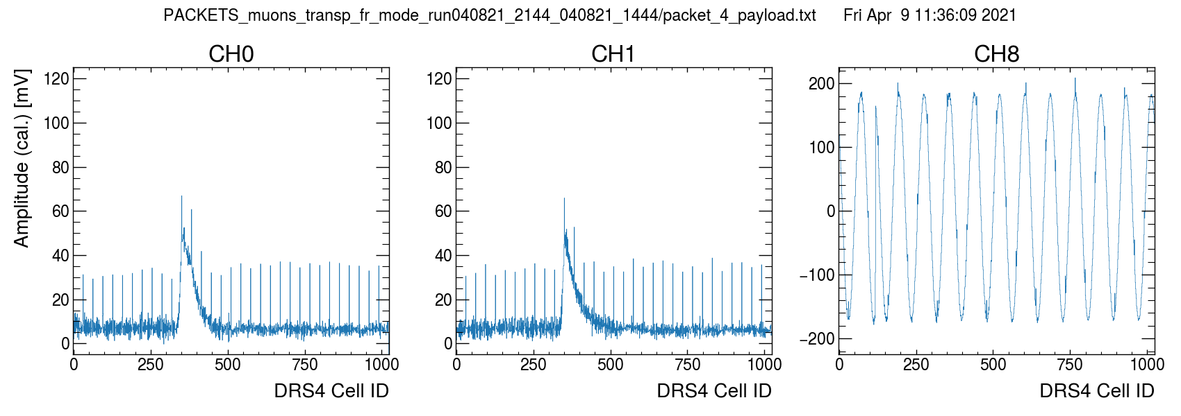
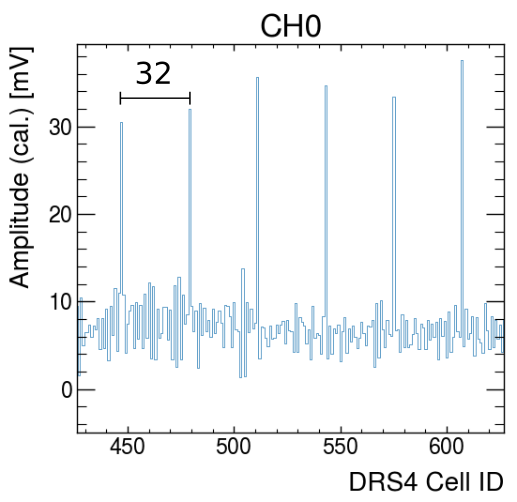
After I modify some clock settings, things seem to improve dramatically, and the spike behavior changes
- ADC and SR CLK = 15 MHz, 0 deg. offset
- Transparent mode = ON
- ROI = ON (just for testing purposes)
- Add 1.064 ns skew to DRS REF CLK
- NOTE: Unfortunately due to a design mishap, the ADC and FPGA clock use a phase-locked output pair on our clock synthesis chip, so we cannot fine-tune the skew for it.
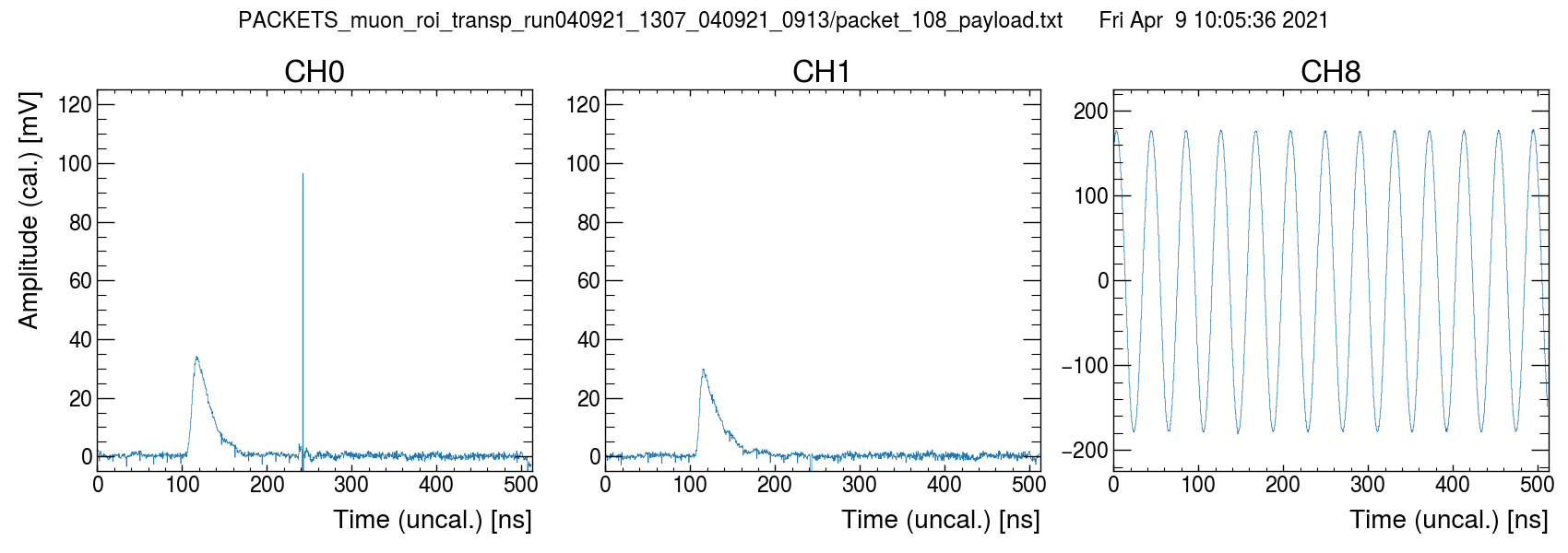
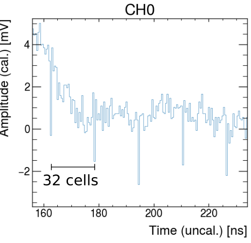
Observed differences
- Spike polarity seems inverted
- Spikes limited to smaller number of cells now?
- Spike amplitude reduced
- Overall baseline variance seems better
- New large positive spike artifact on CH0 that seems inverted on CH1
- CH8 seems unaffected by large spikes?
Artifacts seem related to clock configuration, but I am sort of in the dark on what might be happening from a first-principles point of view. Any tips?
Warm regards,
Sean |
|
825
|
Fri Apr 9 21:38:59 2021 |
Stefan Ritt | Spikes/noise sensitive to clock settings? | elog:824
| Sean Quinn wrote: |
|
Dear DRS4 team,
I'm trying to troubleshoot some odd spike behavior. If I run the ADC and SR CLK at 16 MHz (behavior also seen at 33 MHz) we get very noisy data (post-calibration) with periodic spikes.
In the below plot
- CH0 & CH1 are muon pulses from a scintillator + SiPM detector
- CH8 is a 25 MHz sinewave (in phase with all generated board clocks)
- Transparent mode = ON
- ROI = OFF, "full readout mode", first sample = cell 0
- DRS REFCLK = 1 MHz (2 GS/s)
- ADC & SR CLK = 16 MHz, 0 deg. offset


After I modify some clock settings, things seem to improve dramatically, and the spike behavior changes
- ADC and SR CLK = 15 MHz, 0 deg. offset
- Transparent mode = ON
- ROI = ON (just for testing purposes)
- Add 1.064 ns skew to DRS REF CLK
- NOTE: Unfortunately due to a design mishap, the ADC and FPGA clock use a phase-locked output pair on our clock synthesis chip, so we cannot fine-tune the skew for it.


Observed differences
- Spike polarity seems inverted
- Spikes limited to smaller number of cells now?
- Spike amplitude reduced
- Overall baseline variance seems better
- New large positive spike artifact on CH0 that seems inverted on CH1
- CH8 seems unaffected by large spikes?
Artifacts seem related to clock configuration, but I am sort of in the dark on what might be happening from a first-principles point of view. Any tips?
Warm regards,
Sean
|
|
|
885
|
Fri Jun 24 09:57:36 2022 |
LynseyShun | Spikes/noise sensitive to clock settings? | Hello, I now have periodic spikes in CH0 and CH1 output. How can I eliminate these spikes? I'm sorry I didn't understand your elimination method. Please explain the method in detail. Thank you very much
| Stefan Ritt wrote: |
|
elog:824
| Sean Quinn wrote: |
|
Dear DRS4 team,
I'm trying to troubleshoot some odd spike behavior. If I run the ADC and SR CLK at 16 MHz (behavior also seen at 33 MHz) we get very noisy data (post-calibration) with periodic spikes.
In the below plot
- CH0 & CH1 are muon pulses from a scintillator + SiPM detector
- CH8 is a 25 MHz sinewave (in phase with all generated board clocks)
- Transparent mode = ON
- ROI = OFF, "full readout mode", first sample = cell 0
- DRS REFCLK = 1 MHz (2 GS/s)
- ADC & SR CLK = 16 MHz, 0 deg. offset


After I modify some clock settings, things seem to improve dramatically, and the spike behavior changes
- ADC and SR CLK = 15 MHz, 0 deg. offset
- Transparent mode = ON
- ROI = ON (just for testing purposes)
- Add 1.064 ns skew to DRS REF CLK
- NOTE: Unfortunately due to a design mishap, the ADC and FPGA clock use a phase-locked output pair on our clock synthesis chip, so we cannot fine-tune the skew for it.


Observed differences
- Spike polarity seems inverted
- Spikes limited to smaller number of cells now?
- Spike amplitude reduced
- Overall baseline variance seems better
- New large positive spike artifact on CH0 that seems inverted on CH1
- CH8 seems unaffected by large spikes?
Artifacts seem related to clock configuration, but I am sort of in the dark on what might be happening from a first-principles point of view. Any tips?
Warm regards,
Sean
|
|
|
|
888
|
Fri Jul 29 17:23:43 2022 |
Stefan Ritt | Spikes/noise sensitive to clock settings? | Look at the DRS4 data sheet, Figure 12. You see there the rising SRCLK pulse which outputs the next analog value. You also see tSAMP which describes the sampling piont (strobe or clock sent to your ADC). The value of tSAMP must be such that the values is sampled at the point where it flattens out, just 2-3 ns BEFORE the next analog sample is clocked out, as written in the text. So you have to phase shift your clock going to SRCLK and the one going to your ADC against each other. This needs adjustment at the ns level, so you need a PLL with fine-valued taps, so you can shift it in fractions of a ns. What you see is that you sample at the BEGINNING of a new value to be output to the chip. Please also note that most ADCs have an internal delay of their clock (usually called 'aperture') which has to be taken into account. So if your SRCLK and your ADC clock come at the same time (not phase shifted), it might happen that the ADC internal aperture delay caues it to sample the analog signal at the BEGINNING of the new value.
Hope this is clearer now.
Best regards,
Stefan |
|
348
|
Tue May 27 13:46:18 2014 |
Dominik Neise | Spikes in DRS4 data on custom baord. | We see quite some spikes in our DRS4 sampled data in FACT. We see different types of spikes:
- single cell spikes, usually showing a large amplitude of 200mV
- double cell spikes, usually only in the order of 20mV.
- Even triple and quadro cell spikes are rarely seen.
The double cell spikes often occur as symmetrical double cell spikes mirrored at cell 512. quadro cell spikes seem to be nothing else, than connected symmetrical double cell spikes. For the triple cell spikes we have no idea.
Currently we use simple filters to get rid of these spikes, this workes rather well for the large single cell spikes, but with the occurance of tripples and quadros we started to worry about higher multiples and revived our DRS4 spike investigations.
Now I was told, that you Stefan know already where these spikes come from and even a paper exisits. Unfortunately so far I was unable to find it.
I wonder if it is possible to predict the occurance of these spikes, so one does not have to search for them anymore and can get rid of the filters.
Best regards
Dominik |
|
349
|
Tue May 27 16:07:17 2014 |
Stefan Ritt | Spikes in DRS4 data on custom baord. |
| Dominik Neise wrote: |
|
We see quite some spikes in our DRS4 sampled data in FACT. We see different types of spikes:
- single cell spikes, usually showing a large amplitude of 200mV
- double cell spikes, usually only in the order of 20mV.
- Even triple and quadro cell spikes are rarely seen.
The double cell spikes often occur as symmetrical double cell spikes mirrored at cell 512. quadro cell spikes seem to be nothing else, than connected symmetrical double cell spikes. For the triple cell spikes we have no idea.
Currently we use simple filters to get rid of these spikes, this workes rather well for the large single cell spikes, but with the occurance of tripples and quadros we started to worry about higher multiples and revived our DRS4 spike investigations.
Now I was told, that you Stefan know already where these spikes come from and even a paper exisits. Unfortunately so far I was unable to find it.
I wonder if it is possible to predict the occurance of these spikes, so one does not have to search for them anymore and can get rid of the filters.
Best regards
Dominik
|
All I know is that the "20mV" spikes are always symmetrical around cell #512, that they are typically 17.4 mV in height, and that they occur always in all 9 channels simultaneously. They cannot occur in all locations, but there only like 32 possible locations where they can occur. With this information it should be easy to fix them by filtering.
200 mV spikes are new to me. I do not see them in our boards, so it must be related to the board readout and not to the chip.
Best regards,
Stefan
|
|
289
|
Wed Aug 28 13:07:51 2013 |
Andrey Kuznetsov | Some bug fixes and questions | For http://www.psi.ch/drs/DocumentationEN/manual_rev20.pdf:
0 0x02 15..8 board_type 5 for DRS4 USB Evaluation Board 1.1 ---> should instead say Evaluation Board 2.0 ?
I've been reviewing DRS.cpp v4.0.1
1) if(i==100) should be if(i==1000) in function int DRSBoard::SetFrequency(double demand, bool wait)
Otherwise if PLL did not lock, i = 1000, and the if statement is evaluating it against 100, not 1000 so it never gets triggered and the error goes unnoticed.
if (wait) {
StartDomino();
for (i=0 ; i<1000 ; i++)
if (GetStatusReg() & BIT_PLL_LOCKED0)
break;
SoftTrigger();
if (i==100) {
printf("PLL did not lock for frequency %lf\n", demand);
return 0;
}
}
2) int DRSBoard::RegulateFrequency(double demand) does not seem to work at all, the frequency does not lock for either 2 or 5 GHz, tested using DRS4 v2.0 eval board with DRS v4.0.1 and v2.0.1 software's drscl tool.
3) In int DRSBoard::SetTriggerDelayPercent(int delay) and int DRSBoard::SetTriggerDelayNs(int delay), what is the purpose of Read and setting of "reg" if it's not being used or exported anywhere else outside of that function? Seems like Read and reg are called for nothing.
Read(T_CTRL, ®, REG_TRG_DELAY, 2);
reg = (reg & 0xFF00) | ticks;
Write(T_CTRL, REG_TRG_DELAY, &ticks, 2);
Also, I don't understand why in int DRSBoard::SetSyncDelay(int ticks), the code changes to Read(T_CTRL, ®, REG_TRG_DELAY, 2);
reg = (reg & 0xFF) | (ticks << 8);
Write(T_CTRL, REG_TRG_DELAY, ®, 2);
In particular, reg = (reg & 0xFF00) | ticks; and reg = (reg & 0xFF) | (ticks << 8); I'm not really sure but doesn't Read() with size 2 return a value that has a maximum value of 0xFF, or 8bits? But ticks << 8, since ticks == 255 max, makes 255 << 8 => 65280, which is now a 16bit value and size 4. No? I might be wrong here, and if I am then I don't understand what's going on. Can you please explain? In v2.0.1 the ticks were a maximum of 511 or 9bits, why did it change to 8bits?
4) A function is being called incorrectly in GetWave() in DRS.cpp
int DRSBoard::GetWave(unsigned int chipIndex, unsigned char channel, float *waveform)

{
   return GetWave(chipIndex, channel, waveform, true, fStopCell[chipIndex], false, 0, true);

}
The return is calling the following overloaded function:
int DRSBoard::GetWave(unsigned int chipIndex, unsigned char channel, float *waveform, bool responseCalib, int triggerCell, int wsr, bool adjustToClock, float threshold, bool offsetCalib)
the problem is that int wsr is not passed to the function and it thus causes implicit conversions where false is being cast into int, 0 into bool, and true into float.
I'll post more if I have any questions or spot any more bugs. |
|
290
|
Thu Sep 5 10:01:00 2013 |
Andrey Kuznetsov | Some bug fixes and questions | #11 0x080589de in DRSBoard::GetWave (this=0xb7456008, chipIndex=0, channel=0 '\000', waveform=0x40f24000, responseCalib=true, triggerCell=207, wsr=0, adjustToClock=false, threshold=1, offsetCalib=true) at src/DRS.cpp:3380
This is calling:
int GetWave(unsigned int chipIndex, unsigned char channel, float *waveform, bool responseCalib, int triggerCell = -1, int wsr = -1, bool adjustToClock = false, float threshold = 0, bool offsetCalib = true);
from DRS.cpp:
return GetWave(chipIndex, channel, waveform, true, fStopCell[chipIndex], false, 0, true);

false=0
true=1

As you can see offsetCalib ends up being defined by default, threshold set to 1 because of true, adjustToClock is false set by 0, wsr is 0 set by false, however threshold is never used with DRS4 eval board. So although it doesn't affect data retrieval, it's just dumb luck the function ends up being called with parameters that matter being exactly what they were meant to be.
|
|
291
|
Mon Sep 9 06:49:36 2013 |
Andrey Kuznetsov | Some bug fixes and questions | The DRSCallback *pcb is missing an if statement in the code when DRS Oscilloscope software isn't used when calibrating in function: int DRSBoard::CalibrateTiming(DRSCallback *pcb)
I had to add if (pcb != NULL) before each pcb call, like other functions are using so that the program doesn't segfault when the function is called like b->CalibrateTiming(NULL);
That's the only function that's missing this if statement for DRSCallback *pcb call, and there are 2 calls in this function to pcb that need fixing. |
|
325
|
Wed Jan 15 16:15:00 2014 |
Stefan Ritt | Some bug fixes and questions |
Type 5 is both for board V1.1 and V2. I consider V1.1 obsolete (nobody uses it). I added code 8 for V4 and 9 for V5
| Andrey Kuznetsov wrote: |
|
1) if(i==100) should be if(i==1000) in function int DRSBoard::SetFrequency(double demand, bool wait)
Otherwise if PLL did not lock, i = 1000, and the if statement is evaluating it against 100, not 1000 so it never gets triggered and the error goes unnoticed.
if (wait) {
StartDomino();
for (i=0 ; i<1000 ; i++)
if (GetStatusReg() & BIT_PLL_LOCKED0)
break;
SoftTrigger();
if (i==100) {
printf("PLL did not lock for frequency %lf\n", demand);
return 0;
}
}
|
Absolutely correct, I changed it in the current software.
| Andrey Kuznetsov wrote: |
|
2) int DRSBoard::RegulateFrequency(double demand) does not seem to work at all, the frequency does not lock for either 2 or 5 GHz, tested using DRS4 v2.0 eval board with DRS v4.0.1 and v2.0.1 software's drscl tool.
|
This function is for the old DRS2 chip back in 2003 or so. That chip did not have an on-chip PLL for frequency regulation, so this was done in the FPGA. Just don't us it (who told you to???).
| Andrey Kuznetsov wrote: |
|
3) In int DRSBoard::SetTriggerDelayPercent(int delay) and int DRSBoard::SetTriggerDelayNs(int delay), what is the purpose of Read and setting of "reg" if it's not being used or exported anywhere else outside of that function? Seems like Read and reg are called for nothing.
Read(T_CTRL, ®, REG_TRG_DELAY, 2);
reg = (reg & 0xFF00) | ticks;
Write(T_CTRL, REG_TRG_DELAY, &ticks, 2);
Also, I don't understand why in int DRSBoard::SetSyncDelay(int ticks), the code changes to Read(T_CTRL, ®, REG_TRG_DELAY, 2);
reg = (reg & 0xFF) | (ticks << 8);
Write(T_CTRL, REG_TRG_DELAY, ®, 2);
In particular, reg = (reg & 0xFF00) | ticks; and reg = (reg & 0xFF) | (ticks << 8); I'm not really sure but doesn't Read() with size 2 return a value that has a maximum value of 0xFF, or 8bits? But ticks << 8, since ticks == 255 max, makes 255 << 8 => 65280, which is now a 16bit value and size 4. No? I might be wrong here, and if I am then I don't understand what's going on. Can you please explain? In v2.0.1 the ticks were a maximum of 511 or 9bits, why did it change to 8bits?
|
The register REG_TRG_DELAY contains two 8-bit values, one for the trigger delay, one for the sync delay (which is currently not used). So to set one half of the register containing 16 bits, the register is read (16 bits are read with size 2, since these are two bytes), and the upper or lower 8 bits are replaced with the new value. Then the 16 bits are written back. The firmware in the FPGA does not allow to access only 8 bits of a 16-bit register.
| Andrey Kuznetsov wrote: |
|
4) A function is being called incorrectly in GetWave() in DRS.cpp
int DRSBoard::GetWave(unsigned int chipIndex, unsigned char channel, float *waveform)

{
               return GetWave(chipIndex, channel, waveform, true, fStopCell[chipIndex], false, 0, true);

}
The return is calling the following overloaded function:
int DRSBoard::GetWave(unsigned int chipIndex, unsigned char channel, float *waveform, bool responseCalib, int triggerCell, int wsr, bool adjustToClock, float threshold, bool offsetCalib)
            the problem is that int wsr is not passed to the function and it thus causes implicit conversions where false is being cast into int, 0 into bool, and true into float.
|
That's correct. Fortunately the wrong values for the wsr does not have any influence for "normal" users. It is only used for channel cascading which is not used in the evaluation board. I will fix it in the code anyhow. |
|
326
|
Wed Jan 15 17:02:58 2014 |
Stefan Ritt | Some bug fixes and questions |
| Andrey Kuznetsov wrote: |
|
So although it doesn't affect data retrieval, it's just dumb luck the function ends up being called with parameters that matter being exactly what they were meant to be.
|
Exactly. If I would not have had that dumb luck, I would have seen the problem and fixed it. So it was more like bad luck. |
|