| ID |
Date |
Author |
Subject |
|
880
|
Mon Mar 14 08:59:51 2022 |
Stefan Ritt | Time calibration and the C++ API | Looks like you have the some time calibration, not sure if it's the correct one. Sample the sine wave from the calibration clock, once with and once without the timing calibration, then you will see if all points lie on a smooth line. Left: without timing calibration, right: with proper timing calibration:
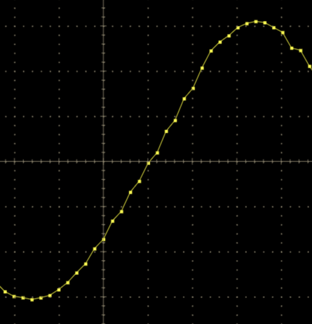 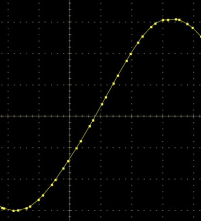
If your points do not lie on a smooth line, you might habe a problem such as the wrong channel for calibration, an offset of 1 in the index of the time array or some other software bug. Measure the same signal with the DRSOsc application and then your code. If the results differ, you have a software problem on your side.
Stefan
|
|
883
|
Tue Apr 12 10:49:27 2022 |
Stefan Ritt | | A3-A0 = 1001 should be all you need to activate OUT0-OUT7. It works in our designs. Maybe double check the address lines with an oscilloscope.
Stefan
| LynseyShun wrote: |
|
Hello, I am Lynsey. now I set A3-A0 to 1001 in ROI mode, but only OUT0 has output, and the other seven channels(OUT1-OUT7) do not output corresponding waveforms.
In ROI mode, can OUT0-OUT7 output sampled waveforms at the same time?
thank you very much
|
|
|
887
|
Fri Jul 29 14:09:35 2022 |
Stefan Ritt | Increase event rate, use ROI mode, and install sw from source in Mac | The firmware from the website always reads 1024 bins. You have to modify it to stop before that, like reading only 128 samples or so. For compiling under MacOSX, this should work, since I do it myself.
Regards,
Stefan
| Jingyu Zhang wrote: |
|
Dear experts,
We are trying to increase the event rate of the DRS4. We looked into the ROI but couldn’t figure out how to run in ROI mode. We are wondering if there is pre-existing firmware for this? We also tried to download and build the software from source on MacOS 12.4 but we were not successful. Can you kindly help us with these?
Best regards,
Jingyu
|
|
|
888
|
Fri Jul 29 17:23:43 2022 |
Stefan Ritt | Spikes/noise sensitive to clock settings? | Look at the DRS4 data sheet, Figure 12. You see there the rising SRCLK pulse which outputs the next analog value. You also see tSAMP which describes the sampling piont (strobe or clock sent to your ADC). The value of tSAMP must be such that the values is sampled at the point where it flattens out, just 2-3 ns BEFORE the next analog sample is clocked out, as written in the text. So you have to phase shift your clock going to SRCLK and the one going to your ADC against each other. This needs adjustment at the ns level, so you need a PLL with fine-valued taps, so you can shift it in fractions of a ns. What you see is that you sample at the BEGINNING of a new value to be output to the chip. Please also note that most ADCs have an internal delay of their clock (usually called 'aperture') which has to be taken into account. So if your SRCLK and your ADC clock come at the same time (not phase shifted), it might happen that the ADC internal aperture delay caues it to sample the analog signal at the BEGINNING of the new value.
Hope this is clearer now.
Best regards,
Stefan |
|
891
|
Tue Sep 27 10:37:11 2022 |
Stefan Ritt | Required Firmware for DRS4 Evaluation Board Version 2.0 | You find each software version at the usual download location at
https://www.dropbox.com/home/drs/drs4/distribution/Download/Linux
The one you need is probably drs-2.1.3.tar.gz which was the last version for the 2.0 board which is now more than 10 years old.
Best,
Stefan
| Kunal Shinde wrote: |
|
Hi, I am working on an old DRS4 board Version "2.0" with firmware revision "13191", I was unable to find this specific firmware source files ("VHDL source code"), please help me where could I find this or send me the required.
Regards,
Kunal
|
|
|
893
|
Tue Sep 27 15:20:55 2022 |
Stefan Ritt | Required Firmware for DRS4 Evaluation Board Version 2.0 | Sorry, got the wrong link. Here the right one: https://www.dropbox.com/sh/clqo7ekr0ysbrip/AACoWJzrQAbf3WiBJHG89bGGa?dl=0
If you untar the archive, you will find a "firmware" subdirectory with all VHDL code.
Stefan
| Kunal Shinde wrote: |
|
I checked the link you provided but it seems that the link doesnt exist please send me valid one.
Regards,
Kunal
| Stefan Ritt wrote: |
|
You find each software version at the usual download location at
https://www.dropbox.com/home/drs/drs4/distribution/Download/Linux
The one you need is probably drs-2.1.3.tar.gz which was the last version for the 2.0 board which is now more than 10 years old.
Best,
Stefan
| Kunal Shinde wrote: |
|
Hi, I am working on an old DRS4 board Version "2.0" with firmware revision "13191", I was unable to find this specific firmware source files ("VHDL source code"), please help me where could I find this or send me the required.
Regards,
Kunal
|
|
|
|
|
896
|
Mon Oct 24 12:50:24 2022 |
Stefan Ritt | Channel Cascading Option in the 2048-bin | The board is delivered in one or the other mode and not meant to be changed by the user, since this requires very delicate soldering which is not easy. If you try anyhow, you loose the quarantee. You can send the board back to the manufacturer for the modification, but this costs quite some moeny.
Best regards,
Stefan
| Phan Van Chuan wrote: |
|
Dear Stefan,
We are using DRS4 evaluation board version 5.1 and firmware version 30000 (as the picture attached). Now, I am in need one channel with length 2048 bin. However, I can't find the resistors R99, ... ,R106 on the hardware of evaluation board; it seems my DRS4 evaluation board doesn't use 2048 bins per channel.
Our question is, can we repair this hardware to read 2048 bins/channel? if that is possible please let me know what to add on hardware/software of DRS4 evaluation.
Best regards.
Phan Van Chuan.
|
|
|
897
|
Mon Feb 6 13:28:28 2023 |
Stefan Ritt | DRS4 installation via tar in ubuntu not working | I fixed the described error. Can you try the new version from https://bitbucket.org/ritt/drs4eb/commits/80b3af753ed32eb365725f0f3244a4109347c01b
| Sebastian Infante wrote: |
|
Hello i cant install any the last versions that i downloaded from the dropbox, i can untar the file called drs-5.0.6 and when i type "make" while inside the extracted folder that starts working properly till a point and i get an error, its worth mention that i installed wxWidgets and could make a simple hello world that worked properly in wxWidgets.
The error that i get is the next one:
inlined from ‘bool ResponseCalibration::ReadCalibrationV4(unsigned int)’ at src/DRS.cpp:7224:35:
/usr/include/x86_64-linux-gnu/bits/string_fortified.h:95:34: warning: ‘char* __builtin___strncpy_chk(char*, const char*, long unsigned int, long unsigned int)’ specified bound depends on the length of the source argument [-Wstringop-truncation]
95 | return __builtin___strncpy_chk (__dest, __src, __len,
| ~~~~~~~~~~~~~~~~~~~~~~~~^~~~~~~~~~~~~~~~~~~~~~
96 | __glibc_objsize (__dest));
| ~~~~~~~~~~~~~~~~~~~~~~~~~
src/DRS.cpp: In member function ‘bool ResponseCalibration::ReadCalibrationV4(unsigned int)’:
src/DRS.cpp:4767:11: note: length computed here
4767 | strncpy(calibrationDirectoryPath, fCalibDirectory, strlen(fCalibDirectory));
| ~~~~~~~^~~~~~~~~~~~~~~~~~~~~~~~~~~~~~~~~~~~~~~~~~~~~~~~~~~~~~~~~~~~~~~~~~~~
In file included from /usr/include/string.h:535,
from /usr/local/include/wx-3.3/wx/string.h:30,
from /usr/local/include/wx-3.3/wx/memory.h:15,
from /usr/local/include/wx-3.3/wx/object.h:19,
from /usr/local/include/wx-3.3/wx/wx.h:15,
from src/DRS.cpp:15:
In function ‘char* strncpy(char*, const char*, size_t)’,
inlined from ‘void DRSBoard::GetCalibrationDirectory(char*)’ at src/DRS.cpp:4767:11,
inlined from ‘bool ResponseCalibration::ReadCalibrationV3(unsigned int)’ at src/DRS.cpp:7066:35:
/usr/include/x86_64-linux-gnu/bits/string_fortified.h:95:34: warning: ‘char* __builtin___strncpy_chk(char*, const char*, long unsigned int, long unsigned int)’ specified bound depends on the length of the source argument [-Wstringop-truncation]
95 | return __builtin___strncpy_chk (__dest, __src, __len,
| ~~~~~~~~~~~~~~~~~~~~~~~~^~~~~~~~~~~~~~~~~~~~~~
96 | __glibc_objsize (__dest));
| ~~~~~~~~~~~~~~~~~~~~~~~~~
src/DRS.cpp: In member function ‘bool ResponseCalibration::ReadCalibrationV3(unsigned int)’:
src/DRS.cpp:4767:11: note: length computed here
4767 | strncpy(calibrationDirectoryPath, fCalibDirectory, strlen(fCalibDirectory));
| ~~~~~~~^~~~~~~~~~~~~~~~~~~~~~~~~~~~~~~~~~~~~~~~~~~~~~~~~~~~~~~~~~~~~~~~~~~~
g++ -g -O2 -Wall -Wuninitialized -fno-strict-aliasing -Iinclude -I/usr/local/include -DOS_LINUX -DHAVE_USB -DHAVE_LIBUSB10 -DUSE_DRS_MUTEX -I/usr/local/lib/wx/include/gtk3-unicode-3.3 -I/usr/local/include/wx-3.3 -D_FILE_OFFSET_BITS=64 -DWXUSINGDLL -D__WXGTK__ -pthread -c src/averager.cpp
g++ -g -O2 -Wall -Wuninitialized -fno-strict-aliasing -Iinclude -I/usr/local/include -DOS_LINUX -DHAVE_USB -DHAVE_LIBUSB10 -DUSE_DRS_MUTEX -I/usr/local/lib/wx/include/gtk3-unicode-3.3 -I/usr/local/include/wx-3.3 -D_FILE_OFFSET_BITS=64 -DWXUSINGDLL -D__WXGTK__ -pthread -c src/ConfigDialog.cpp
In file included from include/DRSOscInc.h:25,
from src/ConfigDialog.cpp:7:
include/DOFrame.h: In member function ‘bool DOFrame::GetRefclk()’:
include/DOFrame.h:111:46: error: ordered comparison of pointer with integer zero (‘bool*’ and ‘int’)
111 | bool GetRefclk() { return m_refClk > 0; }
| ~~~~~~~~~^~~
make: *** [Makefile:81: ConfigDialog.o] Error 1
|
|
|
899
|
Mon Jun 12 14:22:04 2023 |
Stefan Ritt | Different sampling rates in multi-board configuration | No, that's unfortunately not possible.
Stefan
| Javier Caravaca wrote: |
|
Hello,
Is it possible to have different sampling rates in multi-board configuration? I tried using the scope application but I am unable to change the sampling rate independently.
Best,
Javier.
|
|
|
902
|
Wed Sep 13 13:18:45 2023 |
Stefan Ritt | Input range switch added in Version 2.1.3 | To achieve an input range of -1V to 0V, you need an external buffer which can shift this range into the DRS4 range of -0.5V to +0.5V. This external buffer has then to operate with bipolar power supplies, like -2.5V to +2.5V, which are not present on the evaluation board.
Best regards,
Stefan |
|
904
|
Wed Oct 25 19:47:23 2023 |
Stefan Ritt | WaveDREAM Design | No. This is a proprietary design.
Best,
Stefan |
|
907
|
Thu Feb 22 10:37:03 2024 |
Stefan Ritt | Simulation of FPGA | The Cypress has its own firmware, contained in the distribution under firmware/CY7C68013A/drs_eval.c. There you can see how the data is fetched. I kind of forgot how exactly it worked, since I wrote that code back in 2011. But most if the Cypress code is just the configuration of the USB, the communication with the FPGA is kind of straight forward in the Cypress implementation. But you have to read the manual of that chip to understand it.
Unfrtunately there is no full testbench for the firmware, since I didn't have a VHDL Model of the Cypress, so I implemente dit the "hard" way ;-)
Best,
Stefan
| Rod McInnis wrote: |
|
Hello:
A bit of background: I am working on a project that is utilizing the DRS4 Evaluation board as a prototype platform for a dedicated, special use capture. We will only be utilizing one channel of the ADC capture, and the 1024 samples is more than enough.
What I will need to do, however, is do some preprocessing on the incoming ADC data, running some calculation on the fly, possibly some filtering and other transformations before putting the data into the FPGA block memory for transfer to the host via the Cypress USB interface. I will be modifying the "drs4_eval5" VHDL file and doing a new FPGA build.
It will be essential that I be able to simulate this, from the ADC input to the data flow to the Cypress chip. I have "eval board files" which includes the VHDL source files, Xilinxe ISE project files and some very basic simulation testbenches.
Unfortunately, the simulation testbenches call out a "drs4_eval1" module while the Xilinx project uses a "drs4_eval5" module, and the module ports are a little different. I think I can work around that, however. I have run the simulatilon "drs4_eval1_tb", which does a simple write to a Control Register. I need to expand this simulation so that it will initiate a full capture and then transfer the data from the RAM to the Cypress chip.
What I am most confused about is how the Cypress chip sucks out the data from the FPGA block ram. I would expect it to use a burst mode data transfer rather than the cumbersom CSR read/write, but I haven't found any documentation on how this interface works.
Q1: Is there a simulation testbench file available that does the 1024 sample data transfer?
Q2: Is there a waveform diagram that shows the protocol / signal handshake between the FPGA and Cypress chip for this data transfer?
Thank you
Rod McInnis
|
|
|
913
|
Mon Jan 6 12:52:23 2025 |
Stefan Ritt | Problem with C++ script to use DRS4 evaluation board. Not taking data. | 1. Transparent mode is not needed for the hardware trigger, no idea why the code is there. You can probably remove it.
2. EnableTCal is only for the sake of having some waveforms at the input. Indeed you have to disable it to sample real signals.
3. EnableTrigger() is there to enable the hardware trigger. The flag2 is ther for historical reasons (used in older versions of the board).
4. You figured that out already yourself.
5. The functions CalibrateVolt() and CalibrateTiming() are the ones which get called if you click on volt and time calibration in the DRSOsc application. The calibration is store on the evaluation board, so you do not have to call them in your program.
| Matias Henriquez wrote: |
|
Hello, some updates:
4. I was able to capture correct waveforms using c++ code. I needed to use the function SetTriggerDelayNs() to properly capture my waveforms.
5. I noticed that the drsosc program source code uses the functions: CalibrateVolt() and CalibrateTiming() for performing calibration. For these to work, is it necessary to use EnableAcal() and EnableTcal() functions right?
I'd appreciate if you can still give some insights about 1,2 and 3. Thank you!
| Matias Henriquez wrote: |
|
Hello,
I need to write a script in C++ to take data using the DRS4 evaluation board v4. For that, I used the drs_exam.cpp example as a reference. This is my code (see attachement 2), which is very similar to the provided example, however the difference is that I need to trigger on CH1 OR CH2. In the next version I will need to trigger with an OR in all channels.
The problem is, my code gets stuck in waiting for trigger or only 1 event occurs (event 0). I read that event and it doesn't even go above 30mV, which was the threshold I set. There are some questions I have:
- Why Transparent mode is activated for Hardware Trigger?
- Why EnableTCal is activated? is the drs4_exam example based acquires the 100MHz reference just for the sake of the example? or is just a time calibration routine?
- Can someone explain the function EnableTrigger(flag1,flag2) in boardType 8? it si not clear to me how the trigger is enabled.
- To check that my input signals are correct, I run the drsosc application and I can see the signals with no problem (see attachement 1). However I noticed that I had to configure the trigger delay in the drsosc application, and I don't do that in my c++ code. I will try that later.
- How do I perform voltage calibration and time calibration using the c++ functions?
Thank you so much for your help.
|
|
|
|
915
|
Wed Mar 26 08:42:08 2025 |
Stefan Ritt | drs_exam.cpp not compile | You have to link against the DRS.cpp library, plus usblib, plus ... Note there is both a Makefile and a CMakeLists.txt for it. Google how to use "make" or "cmake".
Stefan |
|
920
|
Fri May 9 08:17:50 2025 |
Stefan Ritt | Handling of Write Shift Register and Write Config Register | This is correct. Setting A0-A3 to 0b1101 multiplexes the Shift Write Register to SROUT, so you will either a "0" or a "1" depending on which of the two channels was written last.
Your segmented capture does unfortunately not work. Due to a bug in the silicon, the first (e.g. even) written channel gets half overwritten when you start sampling the second (odd) channel. I should remove that from the documentation.
Furthermore, reading the chip while writing on the "other side" introduces quite some additional noise. The recommended way to do simultaneous reading and writing is therefore to use two separate DRS4 chips and split the input signals to both chips, then read from one chip while writing to the other chip. This keeps the crosstalk at a minimum and both chips run at full performance.
Stefan
| Jonathan Bradshaw wrote: |
|
Hi all
We're building a product which will use two different operating modes; firstly a long capcture using channel daisy chaining (2048 samples) and secondly a segmented capture (2 separate captures of 1024 samples each).
For the long capture, I'm looking to capture 2048 samples for 4 channels. Therefore I configure the Write Shift Register to 0b01010101 and the Write Config Register to 0b11111111. During capture with DWRITE=1 the Write Shift Register will update. Am I correct that once the capture is done and DWRITE=0, I can set A3..0 to 0b1101 and simply read the value of WSROUT to tell the difference?
For the segmented capture, I'm looking to capture 1024 samples for 4 channels on a first tirgger pulse, followed by 1024 samples for 4 channels on a second pulse. Therefore I configure the Write Shift Register to 0b11111111 and the Write Config Register to 0b01010101 and set DWRITE=0 to capture. After the first trigger I set DWRITE=0 and need to update the Write Config Register. Do I need to write in a whole 8 bits to the Write Config Register (i.e. 0b10101010), or can I just shift in a single new bit (value 0b0)?
|
|
|
921
|
Fri May 9 08:26:17 2025 |
Stefan Ritt | Clarification of full channel readout | The full readout mode is not really recommended since you have to pull out the stop position separately. Just do the ROI readout using the RSRLOAD signal, and then do 1024 samples, which also gives you the full waveform, but also the stop position in a single readout cyclce. The "full readout mode" is more there for "historical reasons", but nobody really uses it any more.
If you are interested in all details of the control signals, I propose you have a look at the VHDL code which comes with the software distribution. It's contained in the "firmware" subdirectoy and called drs4_eval5_app.vhd
Stefan
| Jonathan Bradshaw wrote: |
|
Hi all
We're working on a new product using the DRS4 IC, and want to do a full readout from cell 0 (not just Region of Interest). I have a couple of questions I hope you can help me with:
- We plan to do a full readout sequence, starting at cell 0. Part of that sequence includes pulsing RSRLOAD and reading out the stop position as shown in v0.9 datasheet Figure 15. What should the DRS4 address bits A3..0 be set to for reading out the stop position? (I’m assuming it’s 1011 ‘Address Read Shift Register’)
- What is the output delay from the falling edge of SRCLK to valid data at SROUT?
- For channel readout, we pulse SRCLK to advance the read shift register. The diagram shown in v0.9 datasheet Figure 12 appears to show that the analog output is updated on the rising edge of SRCLK. Is this correct or have I misread the diagram? (Other shift register transfers are clocked on the falling edge
- The DRS4 v0.9 datasheet Figure 7 shows that the Configuration register is clocked on the falling edge of SRCLK. Just below that is the text “The new register content becomes immediately active at the eighth rising edge of the SRCLK signal.” Should that perhaps read ‘… the eighth falling edge of the SRCLK signal’?
|
|
|
923
|
Tue May 13 08:51:34 2025 |
Stefan Ritt | Handling of Write Shift Register and Write Config Register | Yes this is correct. Anyhow, even if it would be working, you would not be happy with it. After having designed ~10 boards with the DRS4 chip, I learned the hard way that any digital activity on the board during the sampling phase is strictly forbidden. You see crosstalk up to 100's of mV in some cases (with a preamplifier on the board, 10-20mV without preamp). So rule #1 is to keep the board as "quite" as possible when sampling the input. If you would readout the odd channels of the DRS4 during sampling of the even channels, you would probably get so much crosstalk that the samples are almost unusable. Even if you would do this with two DRS4 chips next to each other, you have to make sure to put proper grounding between the two chips, and operate them completely independent (like each one has it's onw contol lines going to the FPGA). Designing such boards is not so easy and takes lots of experience from the layouter.
Stefan
| Jonathan Bradshaw wrote: |
|
Hi Stefan
Just so I'm 100% clear; is there no reliable way to perform 2 segmented captures with a single DRS4 IC?
While not a showstopper, this is a bit disappointing.
| Stefan Ritt wrote: |
|
This is correct. Setting A0-A3 to 0b1101 multiplexes the Shift Write Register to SROUT, so you will either a "0" or a "1" depending on which of the two channels was written last.
Your segmented capture does unfortunately not work. Due to a bug in the silicon, the first (e.g. even) written channel gets half overwritten when you start sampling the second (odd) channel. I should remove that from the documentation.
Furthermore, reading the chip while writing on the "other side" introduces quite some additional noise. The recommended way to do simultaneous reading and writing is therefore to use two separate DRS4 chips and split the input signals to both chips, then read from one chip while writing to the other chip. This keeps the crosstalk at a minimum and both chips run at full performance.
Stefan
| Jonathan Bradshaw wrote: |
|
Hi all
We're building a product which will use two different operating modes; firstly a long capcture using channel daisy chaining (2048 samples) and secondly a segmented capture (2 separate captures of 1024 samples each).
For the long capture, I'm looking to capture 2048 samples for 4 channels. Therefore I configure the Write Shift Register to 0b01010101 and the Write Config Register to 0b11111111. During capture with DWRITE=1 the Write Shift Register will update. Am I correct that once the capture is done and DWRITE=0, I can set A3..0 to 0b1101 and simply read the value of WSROUT to tell the difference?
For the segmented capture, I'm looking to capture 1024 samples for 4 channels on a first tirgger pulse, followed by 1024 samples for 4 channels on a second pulse. Therefore I configure the Write Shift Register to 0b11111111 and the Write Config Register to 0b01010101 and set DWRITE=0 to capture. After the first trigger I set DWRITE=0 and need to update the Write Config Register. Do I need to write in a whole 8 bits to the Write Config Register (i.e. 0b10101010), or can I just shift in a single new bit (value 0b0)?
|
|
|
|
|
298
|
Mon Oct 21 14:43:21 2013 |
Stephane Debieux | DRS4 analog outputs - interfacing DRS4 to AD9222 ADC | Hi,
I wish to interface the DRS4 with the 8-channel ADC AD9222 (or AD9637).
I'm reading from the DRS4 datasheet that "the analog output of the DRS4 chip has been designed to match directly the input of the AD9222". OUT+ output of DRS4 is in the range from 0.8V to 1.8V and OUT- output is shifted by the voltage applied to the O-OFS pin.
The span of the AD9222 ADC core is defined by REFT and REFB which are resp. 1.4V and 0.4V in a typical case (AVDD=1.8V, VREF=1V). My understanding is that the ADC analog inputs must be within the voltage range defined by REFT and REFB and so I don't quite see how this matches the DRS4 outputs.
Can we use the full-scale range indeed? Do we have to use AC-coupling with mid-supply bias? What is the point I missed?
Thank you for your help.
|
|
377
|
Tue Oct 7 14:09:02 2014 |
Stephane Debieux | USB Microcontroller firmware | Hi,
I'm trying to recompile the USB microcontroller firmware starting from the drs_eval.c file but I'm not able to get a .iic file close to the one provided with the eval board. It seems to me that this drs_eval.iic file does not match the drs_eval.c and drs_eval.hex files or that I'm doing something wrong. Could you please help or give me an explanation.
Thank you.
Stephane
|
|
379
|
Mon Oct 13 17:08:40 2014 |
Stephane Debieux | USB Microcontroller firmware |
| Stefan Ritt wrote: |
|
| Stephane Debieux wrote: |
|
Hi,
I'm trying to recompile the USB microcontroller firmware starting from the drs_eval.c file but I'm not able to get a .iic file close to the one provided with the eval board. It seems to me that this drs_eval.iic file does not match the drs_eval.c and drs_eval.hex files or that I'm doing something wrong. Could you please help or give me an explanation.
Thank you.
Stephane
|
I did not touch the firmware since a couple of years, but I can confirm that the drs_eval.iic is the correct firmware file, since we use this one on all of our boards. To program it, you need the Cypress USB Console. You remove the jumper (to detach the EEPROM), then power the board (which then boots from the internal memory), connect to the board via the Cypress console, the put back the jumper while the board is running, then program the file into the EEPROM.
Best,
Stefan
|
Thank you Stefan.
Would that be possible to get the corresponding drs_eval.c source file since I'm assuming the one provided with the eval board is not the right one?
Thank you.
Stephane |
|