ID |
Date |
Author |
Subject |
|
107
|
Wed Jul 21 10:58:20 2010 |
Stefan Ritt | ENOB of DRS |
| Jinhong Wang wrote: |
|
Hi, Stefan, I see in your ppt "Design and performance of 6 GSPS waveform digitizing chip DRS4" , you define DRS4 ENOB as 1Vpp/0.35mv(RMS) = 11.5bit, where, 1Vpp is the linearity input range, and 0.35mv is the rms voltage after offset correction. What I understand is that 0.35mV is obtained from DC offset Correction, hence 11.5 bit is for DC input, am i right? If true, what about ENOB for AC input in the whole analog bandwidth? thanks~
|
The expression ENOB for 1Vpp/0.35mV(RMS) is wrong, but I learned this later. Now I call it SNR. The ENOB is calculated in a more complicated way, see for example http://en.wikipedia.org/wiki/ENOB. If you measure the ENOB without timing correction, it's pretty poor (in the order of 7-8 bits). This is because without timing calibration, a sine input has huge side bands, and the ENOB involves the power of your signal over the power of the side bands. If you do a proper timing calibration, you spectrum gets "sharper", and hence the ENOB increases. But I have to admit that I never measured it carefully, since we are still optimizing the timing calibration. Once we have a perfect timing calibration, I will do it and update the data sheet. |
|
110
|
Tue Oct 12 03:53:37 2010 |
Jinhong Wang | Reference design for DRS4 active input buffer |
| Stefan Ritt wrote: |
|
The design of high frequency differential input stages with the DRS4 is a challenge, since the chip draws quite some current at the input (up to 1 mA at 5 GSPS), which must be sourced by the input buffer. A simple transformer as used in the DRS4 Evaluation Board 2.0 limits the bandwidth to 220 MHz. In meantime two active input stages have been worked out and successfully been tested, both utilizing the THS4508 differential amplifier. The first design is AC-coupled and uses less power, the second design is DC-coupled and uses more power with the benefit of delivering a higher bandwidth.
Both designs use a clamping diode at the input as a protection against high voltage spikes at the input. We used a RCLAMP0502B diode from SEMTECH, but any fast voltage suppressor diode will do the job.
The CMOFS input to the THS4508 set the common mode of the differential amplifier. In the AC version the level is set to mid-rail (2.5V), in the DC version it's set to 1.8V to match the input range of the DRS4.
The CAL+ and CAL- signals are used to bias the inputs to a well-defined DC level and can also be used to calibrate the chip. For bipolar inputs, they are both set to 0.8V. A positive 0.5V input pulse then drives DRS_IN+ to (0.8+0.25)V = 1.05V and DRS_IN- to (0.8-0.25)V = 0.55V. A negative 0.5V pulse then drives then DRS_IN+ to 0.55V and DRS_IN- to 1.05V. With ROFS=1.6V, the full dynamic range of the DRS4 is then used. Note that the THS4508 has a gain of 2, and the input has a -6dB voltage divider to compensate for that. To use other input ranges, such as -1V...0V, the CAL+ and CAL- signals can be adjusted accordingly. Note that the inputs of the DRS4 must always be between 0.1V and 1.5V.
AC-coupled version
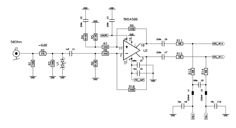
(click to enlarge)
Power supply: +5 V 40 mA
Bandwidth (-3dB): 600 MHz
CMOFS: 2.5 V
Transfer function:
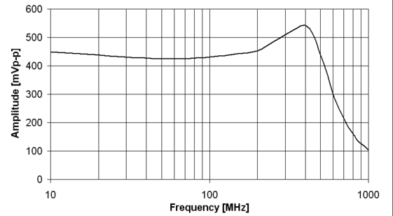
(click to enlarge)
The transfer function was measured by applying a fixed amplitude sine wave to the input, and measuring the peak-to-peak value of the read out waveform with the DRSOsc application.
DC-coupled Version
The DC-coupled version has a slightly higher power consumption since there is a constant current flowing through the output into the DRS4 chip. On the other hand, the bandwidth is a bit higher and the peaking around 400 MHz is a bit smaller. The input is still AC-coupled, so both positive and negative pulses can be accepted.
(click to enlarge)
Power supply: +5 V 115 mA
Bandwidth (-3dB): 800 MHz
CMOFS: 1.8 V
Transfer function:
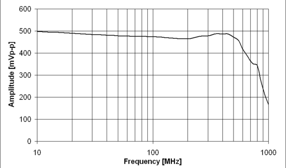
(click to enlarge)
Achievable performance
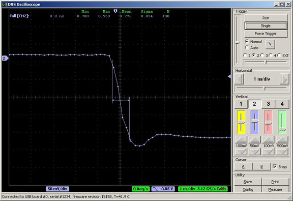
With the active input stage, much faster rise- and fall times can be achieved. Following picture shows a signal from a external clock having a fall time of about 300 ps being recorded with the AC-coupled version of the active input stage. The fall time of the recorded signal is about 800 ps, which is about the minimum which can be achieved with the AC-coupled version. The DC-coupled version achieves about 700ps.
|
Hi, stefan,
In the DC coupled version of the analog drivers for DRS4 input in Eval. Board V3, you mentioned that CMOFS of THS4508 was set to 1.8V to match the input range of DRS4, however, will this clash with the requirements of DRS4 input voltage between 0.1 V ~1.5V ? The output of THS4508 can easily rise beyond 1.5V for CMOFS=1.8V. I also noticed the resister paris R13/R15, R14/R16 was added among the output of THS4508 and the inputs of DRS4, were these resister pairs were used to attenuate the level of THS4508 output signal (a half ? ) to match the input requirements of DRS4? Maybe I have some misunderstanding about it.
|
|
111
|
Tue Nov 16 16:38:06 2010 |
Stefan Ritt | Reference design for DRS4 active input buffer |
| Jinhong Wang wrote: |
|
Hi, stefan,
In the DC coupled version of the analog drivers for DRS4 input in Eval. Board V3, you mentioned that CMOFS of THS4508 was set to 1.8V to match the input range of DRS4, however, will this clash with the requirements of DRS4 input voltage between 0.1 V ~1.5V ? The output of THS4508 can easily rise beyond 1.5V for CMOFS=1.8V. I also noticed the resister paris R13/R15, R14/R16 was added among the output of THS4508 and the inputs of DRS4, were these resister pairs were used to attenuate the level of THS4508 output signal (a half ? ) to match the input requirements of DRS4? Maybe I have some misunderstanding about it.
|
No you are right about that. The THS4508 has a gain of +2, and by using the resistor pairs we do
1) Reduce the gain back to unity
2) Reduce the input DC level from 1.8V to 0.9V to match the input range
3) Terminate the signals at the input of the DRS chip to minimize reflections
I know this is not so obvious from the schematic, so thanks for asking.
- Stefan |
|
112
|
Sat Feb 19 17:25:29 2011 |
S S Upadhya | how to synchronize Sampling frequency of two evaluation boards | Dear sir,
We have two evaluation boards of DRS4. We would like to use 8 inputs to be recorded on a trigger and we would like to find the relative time difference of inputs. So is it possible to synchronize the sampling frequency of the two evaluation boards.
with best regards
S S Upadhya |
|
113
|
Sat Feb 19 22:46:35 2011 |
Stefan Ritt | how to synchronize Sampling frequency of two evaluation boards |
| S S Upadhya wrote: |
|
Dear sir,
We have two evaluation boards of DRS4. We would like to use 8 inputs to be recorded on a trigger and we would like to find the relative time difference of inputs. So is it possible to synchronize the sampling frequency of the two evaluation boards.
with best regards
S S Upadhya
|
No, not in this version. We plan a future version of the evaluation board with clock synchronization, but that board will not be ready before 2-3 months. Anyhow the board is more meant as an evaluation board, to test the chip and develop own electronics, and not to build a complete DAQ system. Note that CAEN distributes now a VME board containing the four DRS4 chips and 32 channels on a board. |
|
114
|
Mon Feb 21 08:10:31 2011 |
Stefan Ritt | how to synchronize Sampling frequency of two evaluation boards |
| Stefan Ritt wrote: |
|
| S S Upadhya wrote: |
|
Dear sir,
We have two evaluation boards of DRS4. We would like to use 8 inputs to be recorded on a trigger and we would like to find the relative time difference of inputs. So is it possible to synchronize the sampling frequency of the two evaluation boards.
with best regards
S S Upadhya
|
No, not in this version. We plan a future version of the evaluation board with clock synchronization, but that board will not be ready before 2-3 months. Anyhow the board is more meant as an evaluation board, to test the chip and develop own electronics, and not to build a complete DAQ system. Note that CAEN distributes now a VME board containing the four DRS4 chips and 32 channels on a board.
|
Well, one thing you can do is to generate an external trigger and send it to the external trigger input of both cards. Then you can determine the time in respect to the trigger point in both boards. But since the trigger cell jitters by 2-3 cells in each chip, the accuracy is limited to about 1-2 ns when running at 2 GS/s. |
|
115
|
Mon Feb 21 12:42:33 2011 |
S S Upadhya | how to synchronize Sampling frequency of two evaluation boards |
| Stefan Ritt wrote: |
|
| Stefan Ritt wrote: |
|
| S S Upadhya wrote: |
|
Dear sir,
We have two evaluation boards of DRS4. We would like to use 8 inputs to be recorded on a trigger and we would like to find the relative time difference of inputs. So is it possible to synchronize the sampling frequency of the two evaluation boards.
with best regards
S S Upadhya
|
No, not in this version. We plan a future version of the evaluation board with clock synchronization, but that board will not be ready before 2-3 months. Anyhow the board is more meant as an evaluation board, to test the chip and develop own electronics, and not to build a complete DAQ system. Note that CAEN distributes now a VME board containing the four DRS4 chips and 32 channels on a board.
|
Well, one thing you can do is to generate an external trigger and send it to the external trigger input of both cards. Then you can determine the time in respect to the trigger point in both boards. But since the trigger cell jitters by 2-3 cells in each chip, the accuracy is limited to about 1-2 ns when running at 2 GS/s.
|
Dear Stefan,
Thanks for the second suggestion. I wanted to do feasibility study of DRS4 application to our requirement in the experiment
Thank you again sir,
Upadhya |
|
116
|
Fri Feb 25 10:13:51 2011 |
Stefan Ritt | Announcement digital pulse processing workshop | Dear colleague,
if you live not so far from Zurich, you might be interested in this workshop:
http://www.xtronix.ch/hep/psi_workshop.htm
This is a combined PSI-CAEN presentation of digitizer hardware including the new V1742 board based on the DRS4 chip. The workshop will also show how digital pulse processing can be used to effectively extract time and energy from detector signals, and thus replace more and more traditional analog electronics. Please register at the above site if you are interested.
Best regards,
Stefan Ritt |
|
117
|
Thu Apr 14 18:23:53 2011 |
Bob Hirosky | Fixes to DOScreen.cpp for recent built on linux | Hello,
I was just building version 3.1.0 and ran into some problems in DOScreen.cpp. Basically the conversions from
char* to wxString were generating "ambiguous overload" errors (in gcc 4.4.3, wx-2.8)
The simple fix is given in the following diff output.
Cheers,
Bob
diff drs-3.1.0_o/src/DOScreen.cpp drs-3.1.0/src
237c237
< wxst = wxString(m_frame->GetOsci()->GetDebugMsg(),wxConvUTF8); //BH
---
> wxst = m_frame->GetOsci()->GetDebugMsg();
246c246
< wxst = wxString(m_debugMsg,wxConvUTF8); //BH
---
> wxst = m_debugMsg;
477c477
< wxst = wxString("AUTO",wxConvUTF8); //BH
---
> wxst = "AUTO";
479c479
< wxst = wxString("TRIG?",wxConvUTF8); //BH
---
> wxst = "TRIG?";
|
|
118
|
Fri Apr 15 08:28:54 2011 |
Stefan Ritt | Fixes to DOScreen.cpp for recent built on linux | > Hello,
>
> I was just building version 3.1.0 and ran into some problems in DOScreen.cpp. Basically the conversions from
> char* to wxString were generating "ambiguous overload" errors (in gcc 4.4.3, wx-2.8)
>
> The simple fix is given in the following diff output.
>
> Cheers,
>
> Bob
>
> diff drs-3.1.0_o/src/DOScreen.cpp drs-3.1.0/src
> 237c237
> < wxst = wxString(m_frame->GetOsci()->GetDebugMsg(),wxConvUTF8); //BH
> ---
> > wxst = m_frame->GetOsci()->GetDebugMsg();
> 246c246
> < wxst = wxString(m_debugMsg,wxConvUTF8); //BH
> ---
> > wxst = m_debugMsg;
> 477c477
> < wxst = wxString("AUTO",wxConvUTF8); //BH
> ---
> > wxst = "AUTO";
> 479c479
> < wxst = wxString("TRIG?",wxConvUTF8); //BH
> ---
> > wxst = "TRIG?";
>
Thanks for mentioning this. I always overlook this because I develop under Windows where this warning does not show
up. I fixed that in the current version. Usually I just use _T() instead wxString() because this is shorter and
recommended by the developers.
Cheers, Stefan. |
|
119
|
Wed Jun 1 09:57:43 2011 |
Martin Petriska | Removing spikes | I have DSR4 eval board. Found that there are spikes in channels. Procedure Osc::RemoveSpikes to remove them looks litlle dificult. There is simple way, if you doesnt need to measure all 4 channels.Spikes are in all channels, and it looks like they are same in time and value between channels. To remove them, if you are not using one channel, substract that unused channel with spikes from used channel and your data will be without spikes. If you need all 4 inputs, then may be channel 9 could be substracted. |
|
120
|
Thu Jun 2 21:01:29 2011 |
Stefan Ritt | Removing spikes |
| Martin Petriska wrote: |
|
I have DSR4 eval board. Found that there are spikes in channels. Procedure Osc::RemoveSpikes to remove them looks litlle dificult. There is simple way, if you doesnt need to measure all 4 channels.Spikes are in all channels, and it looks like they are same in time and value between channels. To remove them, if you are not using one channel, substract that unused channel with spikes from used channel and your data will be without spikes. If you need all 4 inputs, then may be channel 9 could be substracted.
|
Indeed that's what I had before. If you don't need the 9th channels, you can use it to identify the spikes. But we have applications where we need all 9 channels. That's why I made Osc::RemoveSpikes a bit more complicated, so it will still work when all 9 channels are used. This new version is release 3.1.0. If you just blindly subtract the 9th channel, your noise could increase by a sqrt(2). |
|
121
|
Mon Jul 4 05:06:00 2011 |
Jinhong Wang | Fixed Patter Timing Jitter |
| Stefan Ritt wrote: |
|
| Jinhong Wang wrote: |
|
Hi Stefan, can you give some suggestions on determination of fixed pattern timing jitter of DRS4? Thanks~
|
I will prepare some more detailed description of how to do this in the near future, but we are still learning ourselves constantly how to do that better.
So for the moment I only can recommend you to read the function DRSBoard::CalibrateTiming() and AnalyzeWF(). What you basically do is to define an array of "effective" bin widths t[i]. You start with the nominal bin width (let's say 500ps at 2 GSPS). Now you measure a periodic signal, and look for the zero crossings. If you have a 100 MHz clock, the time between two positive transitions (low-to-high) is 10.000ns. Now you measure the width as seen by the DRS chip, assuming the effective bin widths. The exact zero crossing you interpolate between two samples to improve the accuracy. Now you measure something different, let's say 10.1ns. So you know the ~20 bins between the zero crossings are "too wide", but you don't know which one of them is too wide. So you distribute the "too wide" equally between all bins, that is you decrease the effective width of these bins from 500ps to 500-0.1ns/20=499.995 ps. Then you do this iteratively, that is for all cycles in the waveform, and for many (1000's) of recorded waveforms. It is important that the phase of you measured clock is random, so that all bins are covered equally. Then you realize that the solution oscillates, which you can reduce by using a damping factor (called "damping" in my C code). So you do not correct to 499.995ps, but maybe to 499.999ps. If you iterate often enough, the solution kind of stabilizes.
The attached picture shows the result of such a calibration. Green is the effective bin width which in the end only slightly deviates from 500ps. But the "integral temporal nonlinearity" shows a typical shape for the DRS chip. It's defined as
n
Ti[n] = Sum (t[i]-500ps)
i=0
where t[i] is the effective bin width. So Ti[0] is zero by definition, but the deviation around bin 450 can go up to 1ns at 2 GSPS.
Now you can test you calibration, by measuring again the period of your clock. If you do everything correctly and have a low jitter external clock and no noise on your DRS4 power supply voltages, you should see a residual jitter of about 40ps.
Hope this explanation helps a bit. Let me know if I was not clear enough at some points.
- Stefan
|
Hi, Stefan,
I noticed other groups of SCA reported the technique to histogram the zero crossings of a sine wave, and use the bin occupancy to derive the effective aperture width. Recently , I tried this technique to DRS4. In my test, the frequency of the sine wave was selected uncorrelated to the domino frequency.The results were discouraging. Large variations of the domino tap delay was observed. Besides, I also tried to induce an external trigger, which is uncorrelated to the domino frequency, and histogram the stop positions. Unfortunately, large variations were obtained again. I knew there must be something wrong. Do you have any suggestions?
The attachment is the histogram of the stop positions (the vertical axis is the bin count, the horizontal axis is the bin number). First, I calculate the ration of each bin count to the total counts, supposed the total count is 10000, count of bin 37 is 12, so the corresponding ratio is 12/10000=0.0012. The bin delay is derived by multiplying its ratio to the whole domino period (1024*1/FSamp, eg., for 5 GSP/s, this period is 200ps *1024). (The bin delay i observed was with an variation of about 30 ps). If the external trigger is uncorrelated to the domino frequency, so, the stop positions are supposed to distribute equally to all bins? If this is true, can i calculate the bin delay via the histogram ?
thank you~
Wang Jinhong |
| Attachment 1: hist_stoppos.jpg
|

|
|
122
|
Tue Jul 5 10:09:43 2011 |
Stefan Ritt | Fixed Patter Timing Jitter |
| Jinhong Wang wrote: |
|
| Stefan Ritt wrote: |
|
| Jinhong Wang wrote: |
|
Hi Stefan, can you give some suggestions on determination of fixed pattern timing jitter of DRS4? Thanks~
|
I will prepare some more detailed description of how to do this in the near future, but we are still learning ourselves constantly how to do that better.
So for the moment I only can recommend you to read the function DRSBoard::CalibrateTiming() and AnalyzeWF(). What you basically do is to define an array of "effective" bin widths t[i]. You start with the nominal bin width (let's say 500ps at 2 GSPS). Now you measure a periodic signal, and look for the zero crossings. If you have a 100 MHz clock, the time between two positive transitions (low-to-high) is 10.000ns. Now you measure the width as seen by the DRS chip, assuming the effective bin widths. The exact zero crossing you interpolate between two samples to improve the accuracy. Now you measure something different, let's say 10.1ns. So you know the ~20 bins between the zero crossings are "too wide", but you don't know which one of them is too wide. So you distribute the "too wide" equally between all bins, that is you decrease the effective width of these bins from 500ps to 500-0.1ns/20=499.995 ps. Then you do this iteratively, that is for all cycles in the waveform, and for many (1000's) of recorded waveforms. It is important that the phase of you measured clock is random, so that all bins are covered equally. Then you realize that the solution oscillates, which you can reduce by using a damping factor (called "damping" in my C code). So you do not correct to 499.995ps, but maybe to 499.999ps. If you iterate often enough, the solution kind of stabilizes.
The attached picture shows the result of such a calibration. Green is the effective bin width which in the end only slightly deviates from 500ps. But the "integral temporal nonlinearity" shows a typical shape for the DRS chip. It's defined as
n
Ti[n] = Sum (t[i]-500ps)
i=0
where t[i] is the effective bin width. So Ti[0] is zero by definition, but the deviation around bin 450 can go up to 1ns at 2 GSPS.
Now you can test you calibration, by measuring again the period of your clock. If you do everything correctly and have a low jitter external clock and no noise on your DRS4 power supply voltages, you should see a residual jitter of about 40ps.
Hope this explanation helps a bit. Let me know if I was not clear enough at some points.
- Stefan
|
Hi, Stefan,
I noticed other groups of SCA reported the technique to histogram the zero crossings of a sine wave, and use the bin occupancy to derive the effective aperture width. Recently , I tried this technique to DRS4. In my test, the frequency of the sine wave was selected uncorrelated to the domino frequency.The results were discouraging. Large variations of the domino tap delay was observed. Besides, I also tried to induce an external trigger, which is uncorrelated to the domino frequency, and histogram the stop positions. Unfortunately, large variations were obtained again. I knew there must be something wrong. Do you have any suggestions?
The attachment is the histogram of the stop positions (the vertical axis is the bin count, the horizontal axis is the bin number). First, I calculate the ration of each bin count to the total counts, supposed the total count is 10000, count of bin 37 is 12, so the corresponding ratio is 12/10000=0.0012. The bin delay is derived by multiplying its ratio to the whole domino period (1024*1/FSamp, eg., for 5 GSP/s, this period is 200ps *1024). (The bin delay i observed was with an variation of about 30 ps). If the external trigger is uncorrelated to the domino frequency, so, the stop positions are supposed to distribute equally to all bins? If this is true, can i calculate the bin delay via the histogram ?
thank you~
Wang Jinhong
|
One obvious problem in your method is your statistics. If you have n hits in a bin of the histogram, the error of n is sqrt(n). So if you measure 100 hits, this is more like 100+-10 hits. If you want a better precision, you need much higher statistics. I myself never used this method, but I attach a typical nonlinearity curve running at 2 GSPS, sot hat you know what you should expect. I do some smoothing between neighbor bins so that they do not scatter too much. As you can see, the integral nonlinearity goes almost up to +-2 ns. This value is smaller at higher sampling speeds.
- Stefan |
| Attachment 1: nonlinearity.png
|

|
|
123
|
Tue Jul 12 09:49:08 2011 |
Jinhong Wang | Fixed Patter Timing Jitter |
| Stefan Ritt wrote: |
|
| Jinhong Wang wrote: |
|
| Stefan Ritt wrote: |
|
| Jinhong Wang wrote: |
|
Hi Stefan, can you give some suggestions on determination of fixed pattern timing jitter of DRS4? Thanks~
|
I will prepare some more detailed description of how to do this in the near future, but we are still learning ourselves constantly how to do that better.
So for the moment I only can recommend you to read the function DRSBoard::CalibrateTiming() and AnalyzeWF(). What you basically do is to define an array of "effective" bin widths t[i]. You start with the nominal bin width (let's say 500ps at 2 GSPS). Now you measure a periodic signal, and look for the zero crossings. If you have a 100 MHz clock, the time between two positive transitions (low-to-high) is 10.000ns. Now you measure the width as seen by the DRS chip, assuming the effective bin widths. The exact zero crossing you interpolate between two samples to improve the accuracy. Now you measure something different, let's say 10.1ns. So you know the ~20 bins between the zero crossings are "too wide", but you don't know which one of them is too wide. So you distribute the "too wide" equally between all bins, that is you decrease the effective width of these bins from 500ps to 500-0.1ns/20=499.995 ps. Then you do this iteratively, that is for all cycles in the waveform, and for many (1000's) of recorded waveforms. It is important that the phase of you measured clock is random, so that all bins are covered equally. Then you realize that the solution oscillates, which you can reduce by using a damping factor (called "damping" in my C code). So you do not correct to 499.995ps, but maybe to 499.999ps. If you iterate often enough, the solution kind of stabilizes.
The attached picture shows the result of such a calibration. Green is the effective bin width which in the end only slightly deviates from 500ps. But the "integral temporal nonlinearity" shows a typical shape for the DRS chip. It's defined as
n
Ti[n] = Sum (t[i]-500ps)
i=0
where t[i] is the effective bin width. So Ti[0] is zero by definition, but the deviation around bin 450 can go up to 1ns at 2 GSPS.
Now you can test you calibration, by measuring again the period of your clock. If you do everything correctly and have a low jitter external clock and no noise on your DRS4 power supply voltages, you should see a residual jitter of about 40ps.
Hope this explanation helps a bit. Let me know if I was not clear enough at some points.
- Stefan
|
Hi, Stefan,
I noticed other groups of SCA reported the technique to histogram the zero crossings of a sine wave, and use the bin occupancy to derive the effective aperture width. Recently , I tried this technique to DRS4. In my test, the frequency of the sine wave was selected uncorrelated to the domino frequency.The results were discouraging. Large variations of the domino tap delay was observed. Besides, I also tried to induce an external trigger, which is uncorrelated to the domino frequency, and histogram the stop positions. Unfortunately, large variations were obtained again. I knew there must be something wrong. Do you have any suggestions?
The attachment is the histogram of the stop positions (the vertical axis is the bin count, the horizontal axis is the bin number). First, I calculate the ration of each bin count to the total counts, supposed the total count is 10000, count of bin 37 is 12, so the corresponding ratio is 12/10000=0.0012. The bin delay is derived by multiplying its ratio to the whole domino period (1024*1/FSamp, eg., for 5 GSP/s, this period is 200ps *1024). (The bin delay i observed was with an variation of about 30 ps). If the external trigger is uncorrelated to the domino frequency, so, the stop positions are supposed to distribute equally to all bins? If this is true, can i calculate the bin delay via the histogram ?
thank you~
Wang Jinhong
|
One obvious problem in your method is your statistics. If you have n hits in a bin of the histogram, the error of n is sqrt(n). So if you measure 100 hits, this is more like 100+-10 hits. If you want a better precision, you need much higher statistics. I myself never used this method, but I attach a typical nonlinearity curve running at 2 GSPS, sot hat you know what you should expect. I do some smoothing between neighbor bins so that they do not scatter too much. As you can see, the integral nonlinearity goes almost up to +-2 ns. This value is smaller at higher sampling speeds.
- Stefan
|
Thank you, Stefan. It is really kind of you to offer suggestions or comments on our concern.
Recently, we input a sine wave to our DRS board. DRS works at about 5 GS/s. The frequency varies from 131 MHz to 231MHz. The attached picture shows the reconstructed points of sine wave (vertical is the amplitude, horizontal axis is the point numbers). We noticed that the variation of the length of the zero crossing segments is very large. The max. length is perhaps two times the length of the min. I marked in blue color in the picture. It means the corresponding sampling interval of the max. is two times of that of the min. If this is true, DNL of the DRS sampling interval would be very large. We know, for uniform sampling, the length of the zero crossing segments are assumed to be uniform. Do you have any comments? Thank you~ |
| Attachment 1: 131MHz.jpg
|

|
|
124
|
Wed Jul 13 04:26:52 2011 |
Stefan Ritt | Fixed Patter Timing Jitter |
| Jinhong Wang wrote: |
|
| Stefan Ritt wrote: |
|
| Jinhong Wang wrote: |
|
| Stefan Ritt wrote: |
|
| Jinhong Wang wrote: |
|
Hi Stefan, can you give some suggestions on determination of fixed pattern timing jitter of DRS4? Thanks~
|
I will prepare some more detailed description of how to do this in the near future, but we are still learning ourselves constantly how to do that better.
So for the moment I only can recommend you to read the function DRSBoard::CalibrateTiming() and AnalyzeWF(). What you basically do is to define an array of "effective" bin widths t[i]. You start with the nominal bin width (let's say 500ps at 2 GSPS). Now you measure a periodic signal, and look for the zero crossings. If you have a 100 MHz clock, the time between two positive transitions (low-to-high) is 10.000ns. Now you measure the width as seen by the DRS chip, assuming the effective bin widths. The exact zero crossing you interpolate between two samples to improve the accuracy. Now you measure something different, let's say 10.1ns. So you know the ~20 bins between the zero crossings are "too wide", but you don't know which one of them is too wide. So you distribute the "too wide" equally between all bins, that is you decrease the effective width of these bins from 500ps to 500-0.1ns/20=499.995 ps. Then you do this iteratively, that is for all cycles in the waveform, and for many (1000's) of recorded waveforms. It is important that the phase of you measured clock is random, so that all bins are covered equally. Then you realize that the solution oscillates, which you can reduce by using a damping factor (called "damping" in my C code). So you do not correct to 499.995ps, but maybe to 499.999ps. If you iterate often enough, the solution kind of stabilizes.
The attached picture shows the result of such a calibration. Green is the effective bin width which in the end only slightly deviates from 500ps. But the "integral temporal nonlinearity" shows a typical shape for the DRS chip. It's defined as
n
Ti[n] = Sum (t[i]-500ps)
i=0
where t[i] is the effective bin width. So Ti[0] is zero by definition, but the deviation around bin 450 can go up to 1ns at 2 GSPS.
Now you can test you calibration, by measuring again the period of your clock. If you do everything correctly and have a low jitter external clock and no noise on your DRS4 power supply voltages, you should see a residual jitter of about 40ps.
Hope this explanation helps a bit. Let me know if I was not clear enough at some points.
- Stefan
|
Hi, Stefan,
I noticed other groups of SCA reported the technique to histogram the zero crossings of a sine wave, and use the bin occupancy to derive the effective aperture width. Recently , I tried this technique to DRS4. In my test, the frequency of the sine wave was selected uncorrelated to the domino frequency.The results were discouraging. Large variations of the domino tap delay was observed. Besides, I also tried to induce an external trigger, which is uncorrelated to the domino frequency, and histogram the stop positions. Unfortunately, large variations were obtained again. I knew there must be something wrong. Do you have any suggestions?
The attachment is the histogram of the stop positions (the vertical axis is the bin count, the horizontal axis is the bin number). First, I calculate the ration of each bin count to the total counts, supposed the total count is 10000, count of bin 37 is 12, so the corresponding ratio is 12/10000=0.0012. The bin delay is derived by multiplying its ratio to the whole domino period (1024*1/FSamp, eg., for 5 GSP/s, this period is 200ps *1024). (The bin delay i observed was with an variation of about 30 ps). If the external trigger is uncorrelated to the domino frequency, so, the stop positions are supposed to distribute equally to all bins? If this is true, can i calculate the bin delay via the histogram ?
thank you~
Wang Jinhong
|
One obvious problem in your method is your statistics. If you have n hits in a bin of the histogram, the error of n is sqrt(n). So if you measure 100 hits, this is more like 100+-10 hits. If you want a better precision, you need much higher statistics. I myself never used this method, but I attach a typical nonlinearity curve running at 2 GSPS, sot hat you know what you should expect. I do some smoothing between neighbor bins so that they do not scatter too much. As you can see, the integral nonlinearity goes almost up to +-2 ns. This value is smaller at higher sampling speeds.
- Stefan
|
Thank you, Stefan. It is really kind of you to offer suggestions or comments on our concern.
Recently, we input a sine wave to our DRS board. DRS works at about 5 GS/s. The frequency varies from 131 MHz to 231MHz. The attached picture shows the reconstructed points of sine wave (vertical is the amplitude, horizontal axis is the point numbers). We noticed that the variation of the length of the zero crossing segments is very large. The max. length is perhaps two times the length of the min. I marked in blue color in the picture. It means the corresponding sampling interval of the max. is two times of that of the min. If this is true, DNL of the DRS sampling interval would be very large. We know, for uniform sampling, the length of the zero crossing segments are assumed to be uniform. Do you have any comments? Thank you~
|
The length of the segments is a combination of the sampling jitter and the voltage noise. If you signal contains some noise (and all signals do) it will translate to timing jitter. The DNL of the DRS sampling interval shows a variation from the mean of typically 30%. After you correct for it, it will of course become much smaller. As I said, some people measured 10 ps timing with the DRS4 after careful timing calibration. |
|
125
|
Wed Sep 7 16:45:17 2011 |
Guillaume Blanchard | DRS4 and AD9222 | |
Hello,
I am designing a DAQ board with both DRS4 + AD9222 and a FPGA to monitor.
Do I have to change the default value of O-OFS ?
Does a simple low-pass filter (series resistor + capacitor) on each AD9222 input is enough to limit the noise ?
I am planning to use the (DRS4,AD9222,FPGA) group as both a trigger and digitizing system (as shown in the DRS4 datasheet). The DRS4 will be working at 5Ghz with 8 active channels.
So each channel will have a time depth of 1/5Ghz x 1024 = 204.8ns. So, in order to miss nothing, the ADC latency + the trigger decision must be inferior to 204.8ns, am I correct ?
This leads me to implement on my board the 65Mhz version of the AD9222 as this converter has a 8 clock period latency, i.e. 123ns and it left me 81ns to perform a trigger decision ?
Cordially,
G.Blanchard |
|
126
|
Wed Sep 7 16:56:43 2011 |
Stefan Ritt | DRS4 and AD9222 |
| Guillaume Blanchard wrote: |
|
Hello,
I am designing a DAQ board with both DRS4 + AD9222 and a FPGA to monitor.
Do I have to change the default value of O-OFS ?
Does a simple low-pass filter (series resistor + capacitor) on each AD9222 input is enough to limit the noise ?
I am planning to use the (DRS4,AD9222,FPGA) group as both a trigger and digitizing system (as shown in the DRS4 datasheet). The DRS4 will be working at 5Ghz with 8 active channels.
So each channel will have a time depth of 1/5Ghz x 1024 = 204.8ns. So, in order to miss nothing, the ADC latency + the trigger decision must be inferior to 204.8ns, am I correct ?
This leads me to implement on my board the 65Mhz version of the AD9222 as this converter has a 8 clock period latency, i.e. 123ns and it left me 81ns to perform a trigger decision ?
Cordially,
G.Blanchard
|
I'm not so sure about the temperature stability of the default (DRS4 internal O-OFS) value, that's why I used a precision DAC in my design. But actually I never tried without. Probably the default internal value is good enough if you calibrate each chip (which you do anyhow).
Most designs use no filter between DRS4 and AD9222. Since the DRS4 output is BW limited at around 50 MHz, there is not much you win if you put a 32.5 MHz low pass there. And the PCS gets just so much simpler.
You are right with the latency of the AD9222, this is an issue. From the remaining 81 ns you loose a few going out of the FPGA, you need one or two FPGA clock cycles to make the decision, the DRS4 has also some stopping latency (maybe 10 ns). So you are at the edge. Some people use hardware comparators which are faster than the AD9222, one guy uses even directly an LVDS input of the FPGA "mis-used" as a comparator, where the comparator level (=LVDS negative input) comes from a DAC.
- Stefan |
|
127
|
Wed Sep 7 17:28:25 2011 |
Hannes Friederich | DRS4 and AD9222 |
| Guillaume Blanchard wrote: |
|
Hello,
I am designing a DAQ board with both DRS4 + AD9222 and a FPGA to monitor.
Do I have to change the default value of O-OFS ?
Does a simple low-pass filter (series resistor + capacitor) on each AD9222 input is enough to limit the noise ?
I am planning to use the (DRS4,AD9222,FPGA) group as both a trigger and digitizing system (as shown in the DRS4 datasheet). The DRS4 will be working at 5Ghz with 8 active channels.
So each channel will have a time depth of 1/5Ghz x 1024 = 204.8ns. So, in order to miss nothing, the ADC latency + the trigger decision must be inferior to 204.8ns, am I correct ?
This leads me to implement on my board the 65Mhz version of the AD9222 as this converter has a 8 clock period latency, i.e. 123ns and it left me 81ns to perform a trigger decision ?
Cordially,
G.Blanchard
|
Like Stefan pointed out, your time constraints are quite tight. In those 81 ns, you also need to deserialize the AD9222 output. Unless you implement some really fancy input comparison logic, this will consume another 1-2 ADC clock cycles. Perhaps you should first verify that your FPGA design actually can do its job within those 81 ns. In our system, we sample at only 1-2 GHz and have enough margin to implement really complex triggers in FPGA. But the total latency (ADC + FPGA deserialization) takes 250 ns.
Depending on the application, you do need a low-pass filter. Not only because of the noise, but also in order to be able to trigger reliably. Using fast PMTs for example, you will not be able to see all pulses in full size if the bandwidth is 50 MHz and you're only sampling at 65 MSPS.
Hannes |
|
128
|
Fri Sep 9 09:28:57 2011 |
Guillaume Blanchard | DRS4 and AD9222 | Thank you for your answers,
Another question : Have you ever tried to split the differential signal at the output of the DRS4 chip ? For example to feed both an AD9222 and a diff. amplifier (followed by discriminators) ?
|
|