| ID |
Date |
Author |
Subject |
|
78
|
Wed May 12 11:47:39 2010 |
Jinhong Wang | DRS4 chip model |
| Stefan Ritt wrote: |
|
| Ignacio Diéguez Estremera wrote: |
|
So i guess i won't be able to include drs4 in my simulations :-(. Any other suggestions? Maybe the S-params model you where working on? Anything is better than nothing :-)
|
Please find attached the S-parameters.
|
Hi, we plan to do a time interpolating among the eight channels on a single chip to obtain a maximum 40 GSPS (or, maybe 30 GSPS ) sampling rate. Hence RF behavior of the anlog input is very important for us.
Will you give us some advice on the modeling of the anlog input circuit of the chip? Perhaps just the Spice model of the analog input?
The attached S parameters I found here is for fs =1 GSPS, what about fs=5GSPS?
thanks in advance,
Jinhong Wang (wangjinh@mail.ustc.edu.cn ; alleyor.wang@gmail.com) |
|
91
|
Fri Jun 18 11:31:20 2010 |
Jinhong Wang | DVDD Problem of DRS 4 |
| Stefan Ritt wrote: |
|
| Hao Huan wrote: |
|
| Stefan Ritt wrote: |
|
| Hao Huan wrote: |
|
| Stefan Ritt wrote: |
|
| Hao Huan wrote: |
|
Hi Stefan,
on our board some DRS chips draw a lot of current through DVDD after power-up and heat up significantly--it is true that our board doesn't have weak pull-down resistors at DENABLE and DWRITE output pins of FPGA, so this problem might have been caused by that, but a reinitialization of the Domino circuit doesn't help either. We tried different capacitors at DVDD and it seemed the larger the capacitance, the better the result--with a capacitor larger than 10nF some of the DRS chips could work happily in the normal way while if the capacitor is only 4.7nF all of them got very hot. Would you please provide some suggestions why there should be such a problem?
Thanks a lot!
|
I found that sometimes even a reinitialization fails if the pull-down resistors are missing. So instead playing with capacitors at DVDD, I would just solder two resistors on the board which should fix the problem completely.
|
Thanks! After adding pull-down resistors the voltages come back to normal.
However there is another weird problem that arises: a reset pulse seems unable to set the internal shift registers to default values. For example, after reset without addressing the Config Register the PLL will not try to lock with external reference clock. Even if I explicitly address the Config Register after reset and have the PLL locked, some channels of the chip will give null output during readout while other channels work normally. Could it be that some channels are not initiated properly with the Domino circuit?
|
Something is wrong. I have 800 chips, and they all start up fine. Check with your scope the RESET, DSPEED, DENABLE and DTAP signals. When RESET is applied, DSPEED should go to 2.5 V. When DENABLE goes high, the domino wave is started and you should see DTAP toggle. DSPEED is then lowered by the PLL until DTAP matches your external reference clock. I usually keep DENABLE high all the time after initialization, so the domino wave just continues running.
Another problem could however be the chip readout. If some channel gives null output, it could be that your readout has a problem. Do you use RSRLOAD to initialize the readout sequence?
|
Yes; I used RSRLOAD to trigger readout of all channels in parallel so the asymmetry between channels of the same chip is really a big puzzle. Also during reset DSPEED indeed goes to 2.5V, but after reset the PLL will not try to lock with the external reference clock and lower DSPEED. Instead the Domino circuit just oscillates at the highest frequency by itself.
A more confusing discovery is that the SRIN level before starting the Domino wave could affect the behavior of the PLL. I mean the level of SRIN when the chip is at A="1111" or "1010". Is SRIN supposed to influence the chip even in these standby or transparent modes?
|
Just some ideas:
- Is DENABLE really kept high all the time?
- Is DRESET only applied once during initialization, after that it should stay high
- Does REFCLK+/REFCLK- really toggle at the required sampling speed / 2048?
- Is the REFCLK really a good differential signal? Note that it must be biased properly since the DRS4 inputs are high impedance
- Is the Bit1 in the Config Register really at "1" to enable the PLL?
The only way the SRIN level could affect the PLL is if you address the Config Register (A="1100") and you clock in a few bits with SRCLK.
Have you thought about 'crazy' things such as:
- Defining the DRS4 chip wronly in your CAD software so that the pins are different from what you think?
- Some soldering problem of the DRS4 chips (we had this in the past) so that some pins are not connected at all and others have shorts
I guess you checked most of the things, so I'm just wildly guessing in order to stimulate some thoughts.
The ultimate check would be to get one of the evaluation boards (I sent a few to Jean-Francois Genat some time ago...) and compare the DRS4 signals pin by pin.
|
Hi Stefan
I designed the evaluation board for our experiment. On our boards, I encountered the similar problem when working on the PLL of DRS4. I compared the following two configuration process, which on with PLL locked, the other not,
Process1:
step 1: Set DEnable and DWrite low,
Step2 : Reset DRS4 with a negative pulse of about 900 ns
Step3: Set DEnable high, thus do nothing but wait
I found DRS4 PLL working and locked.
Process 2:
Step 1: Set DEnable and DWrite low,
Step2 : Reset DRS4 with a negative pulse of about 900 ns
Step3: Set Config. Register( "11111111" .of course, this step was not necessary, just to see whether SPI was working properly from DTAP when set to "11111110")
Step4: Set The read shift Register ( full read out mode)
Step5: Set DEnable high,
Step6: Set DWrite high , thus low it , and prepare to read the waveform.
Well, I found in this case, the PLL was not locked, I am sure there was no problem with my SPI configuration process of DRS4.
toggle from DTAP could be viewed, but not stable.
Any Suggestions ?
thanks. |
|
93
|
Sat Jun 19 10:09:18 2010 |
Jinhong Wang | DVDD Problem of DRS 4 |
| Stefan Ritt wrote: |
|
| Jinhong Wang wrote: |
|
Hi Stefan
I designed the evaluation board for our experiment. On our boards, I encountered the similar problem when working on the PLL of DRS4. I compared the following two configuration process, which on with PLL locked, the other not,
Process1:
step 1: Set DEnable and DWrite low,
Step2 : Reset DRS4 with a negative pulse of about 900 ns
Step3: Set DEnable high, thus do nothing but wait
I found DRS4 PLL working and locked.
Process 2:
Step 1: Set DEnable and DWrite low,
Step2 : Reset DRS4 with a negative pulse of about 900 ns
Step3: Set Config. Register( "11111111" .of course, this step was not necessary, just to see whether SPI was working properly from DTAP when set to "11111110")
Step4: Set The read shift Register ( full read out mode)
Step5: Set DEnable high,
Step6: Set DWrite high , thus low it , and prepare to read the waveform.
Well, I found in this case, the PLL was not locked, I am sure there was no problem with my SPI configuration process of DRS4.
toggle from DTAP could be viewed, but not stable.
Any Suggestions ?
thanks.
|
So the main difference, if I understand correctly, is the setting of the Config Register. Actually I never tried that, I always went with the default settings (all "1"). What happens if you write "00000000"? You know Bit1 controls the PLL, maybe there is a bug and the signal needs to be inverted.
|
Hi, Stefan,
The problem was fixed by setting Reg_addr "1001" instead of "1111" when in idle state, I was confused. |
|
94
|
Tue Jun 22 10:50:19 2010 |
Jinhong Wang | Reset of DRS4 | Hi Stefan,
I found DRS draw a lot of current when applied Reset after power on, and the PLL does not work properly. I believe there was something that I misunderstood. So, what will happen when Reset is applied more than once after power on? . Though the chip worked well without a Reset, i want to try to find out what was wrong, for a better understanding of DRS.
best regards!
Jinhong |
|
96
|
Tue Jun 22 11:29:26 2010 |
Jinhong Wang | Reset of DRS4 |
| Stefan Ritt wrote: |
|
| Jinhong Wang wrote: |
|
Hi Stefan,
I found DRS draw a lot of current when applied Reset after power on, and the PLL does not work properly. I believe there was something that I misunderstood. So, what will happen when Reset is applied more than once after power on? . Though the chip worked well without a Reset, i want to try to find out what was wrong, for a better understanding of DRS.
best regards!
Jinhong
|
Have you made sure that DENABLE and DWRITE stays low during the reset?
|
Yes, they are stay low until Reset goes high. the process is as following
Step1: Reset ='1', DEnable ='0', DWrite ='0', Reg_addr ="1111", Rsload='0', Srin ='0'
Step2: Reset='0', the others do not change, the low of the pulse is longer than 10 ns.
Step3: Reset='1', the others do not change, wait for some time
Step4: DEnable ='1' to start the domino. |
|
98
|
Tue Jun 22 11:37:42 2010 |
Jinhong Wang | Reset of DRS4 |
| Stefan Ritt wrote: |
|
| Jinhong Wang wrote: |
|
| Stefan Ritt wrote: |
|
| Jinhong Wang wrote: |
|
Hi Stefan,
I found DRS draw a lot of current when applied Reset after power on, and the PLL does not work properly. I believe there was something that I misunderstood. So, what will happen when Reset is applied more than once after power on? . Though the chip worked well without a Reset, i want to try to find out what was wrong, for a better understanding of DRS.
best regards!
Jinhong
|
Have you made sure that DENABLE and DWRITE stays low during the reset?
|
Yes, they are stay low until Reset goes high. the process is as following
Step1: Reset ='1', DEnable ='0', DWrite ='0', Reg_addr ="1111", Rsload='0', Srin ='0'
Step2: Reset='0', the others do not change, the low of the pulse is longer than 10 ns.
Step3: Reset='1', the others do not change, wait for some time
Step4: DEnable ='1' to start the domino.
|
Ok, then I have no idea. I never tried several reset pulses (actually this is not needed), so I have to reproduce the problem myself and investigate it. Actually in all my designs the reset input is just left open, since the internal initial reset is enough, so I have to modify my design first...
|
Ok ,thank you. |
|
104
|
Mon Jul 19 12:07:04 2010 |
Jinhong Wang | Fixed Patter Timing Jitter | Hi Stefan, can you give some suggestions on determination of fixed pattern timing jitter of DRS4? Thanks~ |
|
106
|
Wed Jul 21 10:46:32 2010 |
Jinhong Wang | ENOB of DRS | Hi, Stefan, I see in your ppt "Design and performance of 6 GSPS waveform digitizing chip DRS4" , you define DRS4 ENOB as 1Vpp/0.35mv(RMS) = 11.5bit, where, 1Vpp is the linearity input range, and 0.35mv is the rms voltage after offset correction. What I understand is that 0.35mV is obtained from DC offset Correction, hence 11.5 bit is for DC input, am i right? If true, what about ENOB for AC input in the whole analog bandwidth? thanks~ |
|
110
|
Tue Oct 12 03:53:37 2010 |
Jinhong Wang | Reference design for DRS4 active input buffer |
| Stefan Ritt wrote: |
|
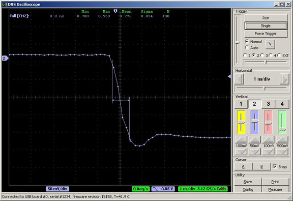
The design of high frequency differential input stages with the DRS4 is a challenge, since the chip draws quite some current at the input (up to 1 mA at 5 GSPS), which must be sourced by the input buffer. A simple transformer as used in the DRS4 Evaluation Board 2.0 limits the bandwidth to 220 MHz. In meantime two active input stages have been worked out and successfully been tested, both utilizing the THS4508 differential amplifier. The first design is AC-coupled and uses less power, the second design is DC-coupled and uses more power with the benefit of delivering a higher bandwidth.
Both designs use a clamping diode at the input as a protection against high voltage spikes at the input. We used a RCLAMP0502B diode from SEMTECH, but any fast voltage suppressor diode will do the job.
The CMOFS input to the THS4508 set the common mode of the differential amplifier. In the AC version the level is set to mid-rail (2.5V), in the DC version it's set to 1.8V to match the input range of the DRS4.
The CAL+ and CAL- signals are used to bias the inputs to a well-defined DC level and can also be used to calibrate the chip. For bipolar inputs, they are both set to 0.8V. A positive 0.5V input pulse then drives DRS_IN+ to (0.8+0.25)V = 1.05V and DRS_IN- to (0.8-0.25)V = 0.55V. A negative 0.5V pulse then drives then DRS_IN+ to 0.55V and DRS_IN- to 1.05V. With ROFS=1.6V, the full dynamic range of the DRS4 is then used. Note that the THS4508 has a gain of 2, and the input has a -6dB voltage divider to compensate for that. To use other input ranges, such as -1V...0V, the CAL+ and CAL- signals can be adjusted accordingly. Note that the inputs of the DRS4 must always be between 0.1V and 1.5V.
AC-coupled version
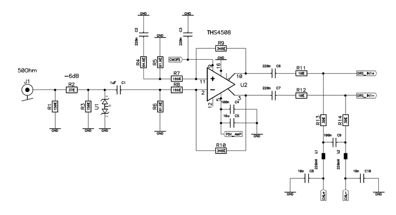
(click to enlarge)
Power supply: +5 V 40 mA
Bandwidth (-3dB): 600 MHz
CMOFS: 2.5 V
Transfer function:
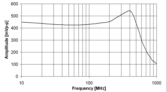
(click to enlarge)
The transfer function was measured by applying a fixed amplitude sine wave to the input, and measuring the peak-to-peak value of the read out waveform with the DRSOsc application.
DC-coupled Version
The DC-coupled version has a slightly higher power consumption since there is a constant current flowing through the output into the DRS4 chip. On the other hand, the bandwidth is a bit higher and the peaking around 400 MHz is a bit smaller. The input is still AC-coupled, so both positive and negative pulses can be accepted.
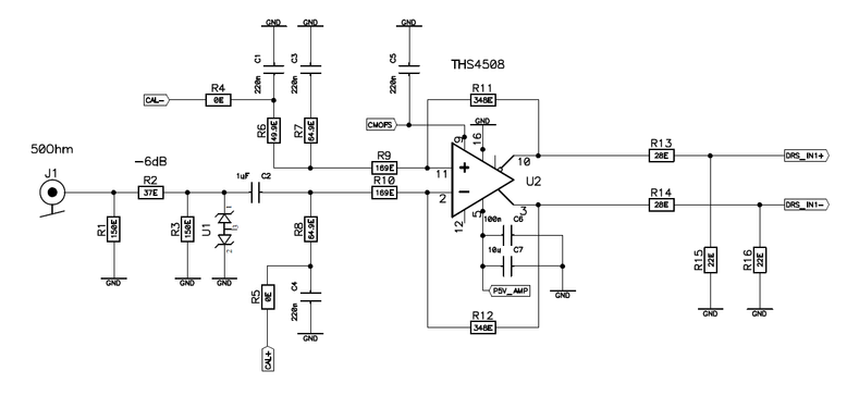
(click to enlarge)
Power supply: +5 V 115 mA
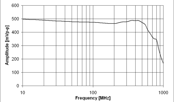
Bandwidth (-3dB): 800 MHz
CMOFS: 1.8 V
Transfer function:
(click to enlarge)
Achievable performance
With the active input stage, much faster rise- and fall times can be achieved. Following picture shows a signal from a external clock having a fall time of about 300 ps being recorded with the AC-coupled version of the active input stage. The fall time of the recorded signal is about 800 ps, which is about the minimum which can be achieved with the AC-coupled version. The DC-coupled version achieves about 700ps.
|
Hi, stefan,
In the DC coupled version of the analog drivers for DRS4 input in Eval. Board V3, you mentioned that CMOFS of THS4508 was set to 1.8V to match the input range of DRS4, however, will this clash with the requirements of DRS4 input voltage between 0.1 V ~1.5V ? The output of THS4508 can easily rise beyond 1.5V for CMOFS=1.8V. I also noticed the resister paris R13/R15, R14/R16 was added among the output of THS4508 and the inputs of DRS4, were these resister pairs were used to attenuate the level of THS4508 output signal (a half ? ) to match the input requirements of DRS4? Maybe I have some misunderstanding about it.
|
|
121
|
Mon Jul 4 05:06:00 2011 |
Jinhong Wang | Fixed Patter Timing Jitter |
| Stefan Ritt wrote: |
|
| Jinhong Wang wrote: |
|
Hi Stefan, can you give some suggestions on determination of fixed pattern timing jitter of DRS4? Thanks~
|
I will prepare some more detailed description of how to do this in the near future, but we are still learning ourselves constantly how to do that better.
So for the moment I only can recommend you to read the function DRSBoard::CalibrateTiming() and AnalyzeWF(). What you basically do is to define an array of "effective" bin widths t[i]. You start with the nominal bin width (let's say 500ps at 2 GSPS). Now you measure a periodic signal, and look for the zero crossings. If you have a 100 MHz clock, the time between two positive transitions (low-to-high) is 10.000ns. Now you measure the width as seen by the DRS chip, assuming the effective bin widths. The exact zero crossing you interpolate between two samples to improve the accuracy. Now you measure something different, let's say 10.1ns. So you know the ~20 bins between the zero crossings are "too wide", but you don't know which one of them is too wide. So you distribute the "too wide" equally between all bins, that is you decrease the effective width of these bins from 500ps to 500-0.1ns/20=499.995 ps. Then you do this iteratively, that is for all cycles in the waveform, and for many (1000's) of recorded waveforms. It is important that the phase of you measured clock is random, so that all bins are covered equally. Then you realize that the solution oscillates, which you can reduce by using a damping factor (called "damping" in my C code). So you do not correct to 499.995ps, but maybe to 499.999ps. If you iterate often enough, the solution kind of stabilizes.
The attached picture shows the result of such a calibration. Green is the effective bin width which in the end only slightly deviates from 500ps. But the "integral temporal nonlinearity" shows a typical shape for the DRS chip. It's defined as
n
Ti[n] = Sum (t[i]-500ps)
i=0
where t[i] is the effective bin width. So Ti[0] is zero by definition, but the deviation around bin 450 can go up to 1ns at 2 GSPS.
Now you can test you calibration, by measuring again the period of your clock. If you do everything correctly and have a low jitter external clock and no noise on your DRS4 power supply voltages, you should see a residual jitter of about 40ps.
Hope this explanation helps a bit. Let me know if I was not clear enough at some points.
- Stefan
|
Hi, Stefan,
I noticed other groups of SCA reported the technique to histogram the zero crossings of a sine wave, and use the bin occupancy to derive the effective aperture width. Recently , I tried this technique to DRS4. In my test, the frequency of the sine wave was selected uncorrelated to the domino frequency.The results were discouraging. Large variations of the domino tap delay was observed. Besides, I also tried to induce an external trigger, which is uncorrelated to the domino frequency, and histogram the stop positions. Unfortunately, large variations were obtained again. I knew there must be something wrong. Do you have any suggestions?
The attachment is the histogram of the stop positions (the vertical axis is the bin count, the horizontal axis is the bin number). First, I calculate the ration of each bin count to the total counts, supposed the total count is 10000, count of bin 37 is 12, so the corresponding ratio is 12/10000=0.0012. The bin delay is derived by multiplying its ratio to the whole domino period (1024*1/FSamp, eg., for 5 GSP/s, this period is 200ps *1024). (The bin delay i observed was with an variation of about 30 ps). If the external trigger is uncorrelated to the domino frequency, so, the stop positions are supposed to distribute equally to all bins? If this is true, can i calculate the bin delay via the histogram ?
thank you~
Wang Jinhong |
| Attachment 1: hist_stoppos.jpg
|

|
|
123
|
Tue Jul 12 09:49:08 2011 |
Jinhong Wang | Fixed Patter Timing Jitter |
| Stefan Ritt wrote: |
|
| Jinhong Wang wrote: |
|
| Stefan Ritt wrote: |
|
| Jinhong Wang wrote: |
|
Hi Stefan, can you give some suggestions on determination of fixed pattern timing jitter of DRS4? Thanks~
|
I will prepare some more detailed description of how to do this in the near future, but we are still learning ourselves constantly how to do that better.
So for the moment I only can recommend you to read the function DRSBoard::CalibrateTiming() and AnalyzeWF(). What you basically do is to define an array of "effective" bin widths t[i]. You start with the nominal bin width (let's say 500ps at 2 GSPS). Now you measure a periodic signal, and look for the zero crossings. If you have a 100 MHz clock, the time between two positive transitions (low-to-high) is 10.000ns. Now you measure the width as seen by the DRS chip, assuming the effective bin widths. The exact zero crossing you interpolate between two samples to improve the accuracy. Now you measure something different, let's say 10.1ns. So you know the ~20 bins between the zero crossings are "too wide", but you don't know which one of them is too wide. So you distribute the "too wide" equally between all bins, that is you decrease the effective width of these bins from 500ps to 500-0.1ns/20=499.995 ps. Then you do this iteratively, that is for all cycles in the waveform, and for many (1000's) of recorded waveforms. It is important that the phase of you measured clock is random, so that all bins are covered equally. Then you realize that the solution oscillates, which you can reduce by using a damping factor (called "damping" in my C code). So you do not correct to 499.995ps, but maybe to 499.999ps. If you iterate often enough, the solution kind of stabilizes.
The attached picture shows the result of such a calibration. Green is the effective bin width which in the end only slightly deviates from 500ps. But the "integral temporal nonlinearity" shows a typical shape for the DRS chip. It's defined as
n
Ti[n] = Sum (t[i]-500ps)
i=0
where t[i] is the effective bin width. So Ti[0] is zero by definition, but the deviation around bin 450 can go up to 1ns at 2 GSPS.
Now you can test you calibration, by measuring again the period of your clock. If you do everything correctly and have a low jitter external clock and no noise on your DRS4 power supply voltages, you should see a residual jitter of about 40ps.
Hope this explanation helps a bit. Let me know if I was not clear enough at some points.
- Stefan
|
Hi, Stefan,
I noticed other groups of SCA reported the technique to histogram the zero crossings of a sine wave, and use the bin occupancy to derive the effective aperture width. Recently , I tried this technique to DRS4. In my test, the frequency of the sine wave was selected uncorrelated to the domino frequency.The results were discouraging. Large variations of the domino tap delay was observed. Besides, I also tried to induce an external trigger, which is uncorrelated to the domino frequency, and histogram the stop positions. Unfortunately, large variations were obtained again. I knew there must be something wrong. Do you have any suggestions?
The attachment is the histogram of the stop positions (the vertical axis is the bin count, the horizontal axis is the bin number). First, I calculate the ration of each bin count to the total counts, supposed the total count is 10000, count of bin 37 is 12, so the corresponding ratio is 12/10000=0.0012. The bin delay is derived by multiplying its ratio to the whole domino period (1024*1/FSamp, eg., for 5 GSP/s, this period is 200ps *1024). (The bin delay i observed was with an variation of about 30 ps). If the external trigger is uncorrelated to the domino frequency, so, the stop positions are supposed to distribute equally to all bins? If this is true, can i calculate the bin delay via the histogram ?
thank you~
Wang Jinhong
|
One obvious problem in your method is your statistics. If you have n hits in a bin of the histogram, the error of n is sqrt(n). So if you measure 100 hits, this is more like 100+-10 hits. If you want a better precision, you need much higher statistics. I myself never used this method, but I attach a typical nonlinearity curve running at 2 GSPS, sot hat you know what you should expect. I do some smoothing between neighbor bins so that they do not scatter too much. As you can see, the integral nonlinearity goes almost up to +-2 ns. This value is smaller at higher sampling speeds.
- Stefan
|
Thank you, Stefan. It is really kind of you to offer suggestions or comments on our concern.
Recently, we input a sine wave to our DRS board. DRS works at about 5 GS/s. The frequency varies from 131 MHz to 231MHz. The attached picture shows the reconstructed points of sine wave (vertical is the amplitude, horizontal axis is the point numbers). We noticed that the variation of the length of the zero crossing segments is very large. The max. length is perhaps two times the length of the min. I marked in blue color in the picture. It means the corresponding sampling interval of the max. is two times of that of the min. If this is true, DNL of the DRS sampling interval would be very large. We know, for uniform sampling, the length of the zero crossing segments are assumed to be uniform. Do you have any comments? Thank you~ |
| Attachment 1: 131MHz.jpg
|

|
|
212
|
Thu Dec 27 00:12:12 2012 |
Jinhong Wang | variation of sampling capacitors | Hi Stefan,
A quick question, what is the typical variation of the sampling capacitors in DRS4? Will this variation be significant to affect your sampling result?
Best,
Jinhong |
|
214
|
Thu Dec 27 18:15:14 2012 |
Jinhong Wang | variation of sampling capacitors |
| Stefan Ritt wrote: |
|
| Jinhong Wang wrote: |
|
Hi Stefan,
A quick question, what is the typical variation of the sampling capacitors in DRS4? Will this variation be significant to affect your sampling result?
Best,
Jinhong
|
The capacitors sample the input voltage, not the charge, so the actual size of the capacitors does not matter on first order (the variations might be in the order of 5%). A bigger effect is the variation of the analog switches in the front of the capacitors, which is about 15%. So the actual bandwidth each cell sees varies by maybe 20% (given by the R and the C), but this comes only into play when sampling steep edges.
Stefan
|
Great to know this! Thanks~
Jinhong |
|
215
|
Fri Feb 1 17:43:48 2013 |
Jinhong Wang | variation of sampling capacitors |
| Jinhong Wang wrote: |
|
| Stefan Ritt wrote: |
|
| Jinhong Wang wrote: |
|
Hi Stefan,
A quick question, what is the typical variation of the sampling capacitors in DRS4? Will this variation be significant to affect your sampling result?
Best,
Jinhong
|
The capacitors sample the input voltage, not the charge, so the actual size of the capacitors does not matter on first order (the variations might be in the order of 5%). A bigger effect is the variation of the analog switches in the front of the capacitors, which is about 15%. So the actual bandwidth each cell sees varies by maybe 20% (given by the R and the C), but this comes only into play when sampling steep edges.
Stefan
|
Great to know this! Thanks~
Jinhong
|
Hi Dr. Stefan,
So the sampling capacitors store the input voltage instead of the charge. What about the readout circuits? I saw there is a buffer followed each sampling capacitor. Do you buffer the charge (like a charge sensitive amplifier) or the voltage? From Fig.12, 14 in datasheet, it seems most probably the readout is a charging or discharging of a capacitor. Could you please add some comments on this?
Cheers,
Jinhong |
|
886
|
Tue Jul 19 02:35:04 2022 |
Jingyu Zhang | Increase event rate, use ROI mode, and install sw from source in Mac | Dear experts,
We are trying to increase the event rate of the DRS4. We looked into the ROI but couldn’t figure out how to run in ROI mode. We are wondering if there is pre-existing firmware for this? We also tried to download and build the software from source on MacOS 12.4 but we were not successful. Can you kindly help us with these?
Best regards,
Jingyu |
|
590
|
Tue Mar 28 21:53:12 2017 |
Jim Freeman | drscl doesn't find eval board but drsosc does (Windows 7) | I cannot find the EVAL board using drscl version 5.06 while the drsosc works fine. I tried 2 different eval boards and 2 different computers and the same effect. I looked under device manager at the libusb and the drs4 was there, and checked the driver which was found to be up to date. |
|
229
|
Tue Mar 26 01:17:59 2013 |
Jill Russek | cascading -- DRS4 Osci.cpp & DRS.cpp |
All I'm trying to do is cascade one input signal, though all available channels, so that I end up with 8*1024 bins per event.
Here is the read out on my board/chip:
Mezz. Board index: 0
DRS type: DRS4
Board type: 8
Serial number: 2249
Firmware revision: 17662
Temperature: 35.2 C
Input range: -0.5V...0.5V
Calibrated range: -0.5V...0.5V
Calibrated frequency: 5.120 GHz
Status reg.: 0000001A
Control reg.: 00000010
DMODE circular
Trigger bus: 00000000
Frequency: 5.120 GHz
What I've tried thus far:
In Osci.cpp, in the method/function SelectSource(int board, int firstChannel, int chnSection), I added a line.. (in bold)
//----------------------------------------------------------------------------------------------------------------------------------------------
if (b->GetBoardType() == 5 || b->GetBoardType() == 7 || b->GetBoardType() == 8) {


             if (chnSection == 2)

                b->SetChannelConfig(0, 8, 4);

             //added

             else if(chnSection == 1)

                 b->SetChannelConfig(0, 8, 2);

             //added

             else

                b->SetChannelConfig(0, 8, 8);
//----------------------------------------------------------------------------------------------------------------------------------------------
I've also tried doing settings such as SetChannelConfig(0, 8, 1); , SetChannelConfig(0, 8, 2); , SetChannelConfig(0, 1, 2); , etc..
Which always ends up making the run fail.. and sometimes I get index errors..
As far as I understanding the program now, this is what I know:
fChannelCascading determines getChannelCascading,

this determines the  if (casc == 2) line in configDialogue.cpp, which sets:

 b->SetChannelConfig(config, 8, 4);


fChannelCascading is being set by:

 switch (nConfigChannels) {

      case 1:

         fChannelConfig = 0x01;

         fChannelCascading = 8;

         break;

      case 2:

         fChannelConfig = 0x11;

         fChannelCascading = 4;

         break;

      case 4:

         fChannelConfig = 0x55;

         fChannelCascading = 2;

         break;

      case 8:

         fChannelConfig = 0xFF;

         fChannelCascading = 1;

         break;

      default:

         printf("Invalid channel configuration\n");

         return 0;

      }


which is being set by nConfigChannels in DRS.cpp, in the method:

SetChannelConfig(int firstChannel, int lastChannel, int nConfigChannels)
SetChannelConfig is being called in the ConfigDialogue.cpp, but the default Osci program is such that you can't do a configuration for a cascade of one signal using all the channels. At least, not that I am aware of.
So what buttons do I need to enable, or what do I need to call, or write, so that I can cascade a signal to end up with 8*1024 bins per event?
This has had me going in circles for weeks, so thank you for your help!!!!
|
|
232
|
Fri Apr 5 02:21:33 2013 |
Jill Russek | cascading -- DRS4 Osci.cpp & DRS.cpp |
| Stefan Ritt wrote: |
|
| Jill Russek wrote: |
|
All I'm trying to do is cascade one input signal, though all available channels, so that I end up with 8*1024 bins per event.
Here is the read out on my board/chip:
Mezz. Board index: 0
DRS type: DRS4
Board type: 8
Serial number: 2249
Firmware revision: 17662
Temperature: 35.2 C
Input range: -0.5V...0.5V
Calibrated range: -0.5V...0.5V
Calibrated frequency: 5.120 GHz
Status reg.: 0000001A
Control reg.: 00000010
DMODE circular
Trigger bus: 00000000
Frequency: 5.120 GHz
What I've tried thus far:
In Osci.cpp, in the method/function SelectSource(int board, int firstChannel, int chnSection), I added a line.. (in bold)
//----------------------------------------------------------------------------------------------------------------------------------------------
if (b->GetBoardType() == 5 || b->GetBoardType() == 7 || b->GetBoardType() == 8) {


                                     if (chnSection == 2)

                                        b->SetChannelConfig(0, 8, 4);

                                     //added

                                     else if(chnSection == 1)

                                         b->SetChannelConfig(0, 8, 2);

                                     //added

                                     else

                                        b->SetChannelConfig(0, 8, 8);
//----------------------------------------------------------------------------------------------------------------------------------------------
I've also tried doing settings such as SetChannelConfig(0, 8, 1); , SetChannelConfig(0, 8, 2); , SetChannelConfig(0, 1, 2); , etc..
Which always ends up making the run fail.. and sometimes I get index errors..
As far as I understanding the program now, this is what I know:
fChannelCascading determines getChannelCascading,

                        this determines the  if (casc == 2) line in configDialogue.cpp, which sets:

                         b->SetChannelConfig(config, 8, 4);


                        fChannelCascading is being set by:

                         switch (nConfigChannels) {

                              case 1:

                                 fChannelConfig = 0x01;

                                 fChannelCascading = 8;

                                 break;

                              case 2:

                                 fChannelConfig = 0x11;

                                 fChannelCascading = 4;

                                 break;

                              case 4:

                                 fChannelConfig = 0x55;

                                 fChannelCascading = 2;

                                 break;

                              case 8:

                                 fChannelConfig = 0xFF;

                                 fChannelCascading = 1;

                                 break;

                              default:

                                 printf("Invalid channel configuration\n");

                                 return 0;

                              }


                        which is being set by nConfigChannels in DRS.cpp, in the method:

                        SetChannelConfig(int firstChannel, int lastChannel, int nConfigChannels)
SetChannelConfig is being called in the ConfigDialogue.cpp, but the default Osci program is such that you can't do a configuration for a cascade of one signal using all the channels. At least, not that I am aware of.
So what buttons do I need to enable, or what do I need to call, or write, so that I can cascade a signal to end up with 8*1024 bins per event?
This has had me going in circles for weeks, so thank you for your help!!!!
|
Sorry for my late reply, I was away for some days.
To use channel cascading, you have to physically connect one input to all eight channels. This is not possible with the evaluation board, you have to make your own board. What you could do however is to split a signal externally and feed it to all four inputs, given that the signal delay is the same for every channel. But then you will hit the hard-wired limit in Osci.cpp. This code was never foreseen to cover 8*1024 bins (since it does not make much sense with the evaluation board). Some arrays are only 2*1024 bins wide, so you would have to rewrite code at many places.
The easiest way to get what you want is to modify drs_exam.cpp. You need SetChannelConfig(0, 8, 1) as you realised correctly, and then you have to retrieve all 8 channels via b->GetWave() and concatenate them correctly.
/Stefan
|
Would it be possible to just hardcode a few lines in the SetChannelConfig in DRS.cpp method as such:
fChannelConfig = 0x01; //gives me eight
d = fChannelConfig | (fDominoMode << 8) | (1 << 9) | (fWSRLoop << 10) | (0xF8 << 8);
Write(T_CTRL, REG_CHANNEL_CONFIG, &d, 2);
fChannelDepth = 8 * (fDecimation ? kNumberOfBins/2 : kNumberOfBins);// gives eight times the bins
then modify the GetWave method/function to include another else if statement similar to "else if (fChannelCascading == 2) {" but would be modifidied for fChannelCascading == 8?
By, "But then you will hit the hard-wired limit in Osci.cpp" do you mean hard-coded? Would changing the hard code just amount to resizing all of the arrays, and replacing all the '2*kNumberBins" with '8*kNumberBins' ?
I'm afraid of drs_exam.cpp because it doesn't come with all the perks of Osci.cpp. It seems less daunting to just modify Osci.cpp then to try understanding everything I need to include in drs_exam.cpp because I'm also using an external trigger, and saving the waveform to an external text file.
Thanks!
/Jill
|
|
235
|
Wed Apr 10 22:41:21 2013 |
Jill Russek | cascading -- DRS4 Osci.cpp & DRS.cpp |
| Stefan Ritt wrote: |
|
| Jill Russek wrote: |
|
Would it be possible to just hardcode a few lines in the SetChannelConfig in DRS.cpp method as such:
fChannelConfig = 0x01; //gives me eight
d = fChannelConfig | (fDominoMode << 8) | (1 << 9) | (fWSRLoop << 10) | (0xF8 << 8);
Write(T_CTRL, REG_CHANNEL_CONFIG, &d, 2);
fChannelDepth = 8 * (fDecimation ? kNumberOfBins/2 : kNumberOfBins);// gives eight times the bins
then modify the GetWave method/function to include another else if statement similar to "else if (fChannelCascading == 2) {" but would be modifidied for fChannelCascading == 8?
By, "But then you will hit the hard-wired limit in Osci.cpp" do you mean hard-coded? Would changing the hard code just amount to resizing all of the arrays, and replacing all the '2*kNumberBins" with '8*kNumberBins' ?
I'm afraid of drs_exam.cpp because it doesn't come with all the perks of Osci.cpp. It seems less daunting to just modify Osci.cpp then to try understanding everything I need to include in drs_exam.cpp because I'm also using an external trigger, and saving the waveform to an external text file.
Thanks!
/Jill
|
Sure it would be possible to code it, but it's not just a few lines. Besides Osci.cpp you have to massage DOScreen.cpp, Measurement.cpp and probably more since they all rely on the array size of the waveform. So if I would do it it would take me probably a couple of days including the debugging, which I don't have right now. Furthermore, as I said you have to combine all eight channels properly. For two channels, it's already pretty complicated (see lines 3537+ in DRS.cpp). I had to make myself a visual scheme in order to understand it correctly, which I attached. For eight channels, the write shift register (WSR) can have values 0-7, depending in which channel you got a trigger. Then you have to sort it out again to get one linear array with the proper order of the fragments. So you see, it's not just changing a few lines of code. In principle it's possible, but it's lots of work.
Best regards,
Stefan
|
Stefan, thanks for your help so far. If I go with your plan A of just modifying drs_exam.cpp, is there a quick way to get it to save the data from the wave, like how osci.cpp spits out an xml file? (Ignoring the cascading aspect for now)
Thanks again :)
/Jill |
|
238
|
Thu Apr 11 23:32:57 2013 |
Jill Russek | cascading -- DRS4 Osci.cpp & DRS.cpp |
| Stefan Ritt wrote: |
|
| Jill Russek wrote: |
|
| Stefan Ritt wrote: |
|
| Jill Russek wrote: |
|
Would it be possible to just hardcode a few lines in the SetChannelConfig in DRS.cpp method as such:
fChannelConfig = 0x01; //gives me eight
d = fChannelConfig | (fDominoMode << 8) | (1 << 9) | (fWSRLoop << 10) | (0xF8 << 8);
Write(T_CTRL, REG_CHANNEL_CONFIG, &d, 2);
fChannelDepth = 8 * (fDecimation ? kNumberOfBins/2 : kNumberOfBins);// gives eight times the bins
then modify the GetWave method/function to include another else if statement similar to "else if (fChannelCascading == 2) {" but would be modifidied for fChannelCascading == 8?
By, "But then you will hit the hard-wired limit in Osci.cpp" do you mean hard-coded? Would changing the hard code just amount to resizing all of the arrays, and replacing all the '2*kNumberBins" with '8*kNumberBins' ?
I'm afraid of drs_exam.cpp because it doesn't come with all the perks of Osci.cpp. It seems less daunting to just modify Osci.cpp then to try understanding everything I need to include in drs_exam.cpp because I'm also using an external trigger, and saving the waveform to an external text file.
Thanks!
/Jill
|
Sure it would be possible to code it, but it's not just a few lines. Besides Osci.cpp you have to massage DOScreen.cpp, Measurement.cpp and probably more since they all rely on the array size of the waveform. So if I would do it it would take me probably a couple of days including the debugging, which I don't have right now. Furthermore, as I said you have to combine all eight channels properly. For two channels, it's already pretty complicated (see lines 3537+ in DRS.cpp). I had to make myself a visual scheme in order to understand it correctly, which I attached. For eight channels, the write shift register (WSR) can have values 0-7, depending in which channel you got a trigger. Then you have to sort it out again to get one linear array with the proper order of the fragments. So you see, it's not just changing a few lines of code. In principle it's possible, but it's lots of work.
Best regards,
Stefan
|
Stefan, thanks for your help so far. If I go with your plan A of just modifying drs_exam.cpp, is there a quick way to get it to save the data from the wave, like how osci.cpp spits out an xml file? (Ignoring the cascading aspect for now)
Thanks again :)
/Jill
|
Well, you have to learn C programming, I won't do it for you. drs_exam.cpp contains already code to write to the ASCII file data.txt, so you just can use that or modify it to your needs.
/Stefan
|
Ha! So then the answer is no, there isn't a ready made function/method to pull out the timing and voltage, like how it was done in osci.cpp. That's all I wanted to know. (Not whether you would write it for me! Only trying to save time!) Thanks!
/Jill |
|