| ID |
Date |
Author |
Subject |
|
700
|
Wed Jun 13 13:23:17 2018 |
Julian Kemp | Maximum analog input voltage | Dear all,
I have been wondering what the maximum analog input voltage for the DRS4 V5 evaluation board is. It came with a sticker indicating that it is "2.5V pk Max". On the other hand, when checking the manual (https://www.psi.ch/drs/DocumentationEN/manual_rev50.pdf), it says maximum allowed is 10V DC or even 30V for short pulses. I foresee an application where I cannot make sure that pulses stay below 2.5V, so the correct value will be quite important for me.
Best,
Julian |
|
702
|
Wed Jun 13 16:34:28 2018 |
Julian Kemp | Maximum analog input voltage | Thank you! That solves my problem.
| Stefan Ritt wrote: |
|
In principle the numbers in the manual are correct. But they relate to pulses of a certain length, because the input protection only works for DC voltage and for pulses which are not too long. Since we could not write this all on the label of the board, we decided to put there 100% safe value as a "warning" to people, meaning that if pulses are above 2.5V, they should look into the manual and read the details.
Stefan
| Julian Kemp wrote: |
|
Dear all,
I have been wondering what the maximum analog input voltage for the DRS4 V5 evaluation board is. It came with a sticker indicating that it is "2.5V pk Max". On the other hand, when checking the manual (https://www.psi.ch/drs/DocumentationEN/manual_rev50.pdf), it says maximum allowed is 10V DC or even 30V for short pulses. I foresee an application where I cannot make sure that pulses stay below 2.5V, so the correct value will be quite important for me.
Best,
Julian
|
|
|
|
631
|
Fri Oct 13 03:39:01 2017 |
Jonathan Wapman | Raspberry Pi Connection Failure | I am currently attempting to use a raspberry pi to connect to the DRS 4 board. I whenever I try to use the DRS Command Line TOol, Revision 21435 to connect to the drs board, I get the error
"musb_open: libusb_open() error -3"
"USB successfully scanned, but no boards found"
"No DRS Boards Found".
I successfully compiled the libusb driver before compiling the drs software 5.0.6, and installed all other listed packages in the install instructions. |
|
918
|
Thu May 8 23:23:19 2025 |
Jonathan Bradshaw | Clarification of full channel readout | Hi all
We're working on a new product using the DRS4 IC, and want to do a full readout from cell 0 (not just Region of Interest). I have a couple of questions I hope you can help me with:
- We plan to do a full readout sequence, starting at cell 0. Part of that sequence includes pulsing RSRLOAD and reading out the stop position as shown in v0.9 datasheet Figure 15. What should the DRS4 address bits A3..0 be set to for reading out the stop position? (I’m assuming it’s 1011 ‘Address Read Shift Register’)
- What is the output delay from the falling edge of SRCLK to valid data at SROUT?
- For channel readout, we pulse SRCLK to advance the read shift register. The diagram shown in v0.9 datasheet Figure 12 appears to show that the analog output is updated on the rising edge of SRCLK. Is this correct or have I misread the diagram? (Other shift register transfers are clocked on the falling edge
- The DRS4 v0.9 datasheet Figure 7 shows that the Configuration register is clocked on the falling edge of SRCLK. Just below that is the text “The new register content becomes immediately active at the eighth rising edge of the SRCLK signal.” Should that perhaps read ‘… the eighth falling edge of the SRCLK signal’?
|
| Attachment 1: Screenshot_2025-05-09_093332.png
|

|
|
919
|
Thu May 8 23:41:03 2025 |
Jonathan Bradshaw | Handling of Write Shift Register and Write Config Register | Hi all
We're building a product which will use two different operating modes; firstly a long capcture using channel daisy chaining (2048 samples) and secondly a segmented capture (2 separate captures of 1024 samples each).
For the long capture, I'm looking to capture 2048 samples for 4 channels. Therefore I configure the Write Shift Register to 0b01010101 and the Write Config Register to 0b11111111. During capture with DWRITE=1 the Write Shift Register will update. Am I correct that once the capture is done and DWRITE=0, I can set A3..0 to 0b1101 and simply read the value of WSROUT to tell the difference?
For the segmented capture, I'm looking to capture 1024 samples for 4 channels on a first tirgger pulse, followed by 1024 samples for 4 channels on a second pulse. Therefore I configure the Write Shift Register to 0b11111111 and the Write Config Register to 0b01010101 and set DWRITE=0 to capture. After the first trigger I set DWRITE=0 and need to update the Write Config Register. Do I need to write in a whole 8 bits to the Write Config Register (i.e. 0b10101010), or can I just shift in a single new bit (value 0b0)? |
|
922
|
Tue May 13 04:10:30 2025 |
Jonathan Bradshaw | Handling of Write Shift Register and Write Config Register | Hi Stefan
Just so I'm 100% clear; is there no reliable way to perform 2 segmented captures with a single DRS4 IC?
While not a showstopper, this is a bit disappointing.
| Stefan Ritt wrote: |
|
This is correct. Setting A0-A3 to 0b1101 multiplexes the Shift Write Register to SROUT, so you will either a "0" or a "1" depending on which of the two channels was written last.
Your segmented capture does unfortunately not work. Due to a bug in the silicon, the first (e.g. even) written channel gets half overwritten when you start sampling the second (odd) channel. I should remove that from the documentation.
Furthermore, reading the chip while writing on the "other side" introduces quite some additional noise. The recommended way to do simultaneous reading and writing is therefore to use two separate DRS4 chips and split the input signals to both chips, then read from one chip while writing to the other chip. This keeps the crosstalk at a minimum and both chips run at full performance.
Stefan
| Jonathan Bradshaw wrote: |
|
Hi all
We're building a product which will use two different operating modes; firstly a long capcture using channel daisy chaining (2048 samples) and secondly a segmented capture (2 separate captures of 1024 samples each).
For the long capture, I'm looking to capture 2048 samples for 4 channels. Therefore I configure the Write Shift Register to 0b01010101 and the Write Config Register to 0b11111111. During capture with DWRITE=1 the Write Shift Register will update. Am I correct that once the capture is done and DWRITE=0, I can set A3..0 to 0b1101 and simply read the value of WSROUT to tell the difference?
For the segmented capture, I'm looking to capture 1024 samples for 4 channels on a first tirgger pulse, followed by 1024 samples for 4 channels on a second pulse. Therefore I configure the Write Shift Register to 0b11111111 and the Write Config Register to 0b01010101 and set DWRITE=0 to capture. After the first trigger I set DWRITE=0 and need to update the Write Config Register. Do I need to write in a whole 8 bits to the Write Config Register (i.e. 0b10101010), or can I just shift in a single new bit (value 0b0)?
|
|
|
|
924
|
Thu May 15 00:01:20 2025 |
Jonathan Bradshaw | Handling of Write Shift Register and Write Config Register | All right, thank you for the clarification.
| Stefan Ritt wrote: |
|
Yes this is correct. Anyhow, even if it would be working, you would not be happy with it. After having designed ~10 boards with the DRS4 chip, I learned the hard way that any digital activity on the board during the sampling phase is strictly forbidden. You see crosstalk up to 100's of mV in some cases (with a preamplifier on the board, 10-20mV without preamp). So rule #1 is to keep the board as "quite" as possible when sampling the input. If you would readout the odd channels of the DRS4 during sampling of the even channels, you would probably get so much crosstalk that the samples are almost unusable. Even if you would do this with two DRS4 chips next to each other, you have to make sure to put proper grounding between the two chips, and operate them completely independent (like each one has it's onw contol lines going to the FPGA). Designing such boards is not so easy and takes lots of experience from the layouter.
Stefan
| Jonathan Bradshaw wrote: |
|
Hi Stefan
Just so I'm 100% clear; is there no reliable way to perform 2 segmented captures with a single DRS4 IC?
While not a showstopper, this is a bit disappointing.
| Stefan Ritt wrote: |
|
This is correct. Setting A0-A3 to 0b1101 multiplexes the Shift Write Register to SROUT, so you will either a "0" or a "1" depending on which of the two channels was written last.
Your segmented capture does unfortunately not work. Due to a bug in the silicon, the first (e.g. even) written channel gets half overwritten when you start sampling the second (odd) channel. I should remove that from the documentation.
Furthermore, reading the chip while writing on the "other side" introduces quite some additional noise. The recommended way to do simultaneous reading and writing is therefore to use two separate DRS4 chips and split the input signals to both chips, then read from one chip while writing to the other chip. This keeps the crosstalk at a minimum and both chips run at full performance.
Stefan
| Jonathan Bradshaw wrote: |
|
Hi all
We're building a product which will use two different operating modes; firstly a long capcture using channel daisy chaining (2048 samples) and secondly a segmented capture (2 separate captures of 1024 samples each).
For the long capture, I'm looking to capture 2048 samples for 4 channels. Therefore I configure the Write Shift Register to 0b01010101 and the Write Config Register to 0b11111111. During capture with DWRITE=1 the Write Shift Register will update. Am I correct that once the capture is done and DWRITE=0, I can set A3..0 to 0b1101 and simply read the value of WSROUT to tell the difference?
For the segmented capture, I'm looking to capture 1024 samples for 4 channels on a first tirgger pulse, followed by 1024 samples for 4 channels on a second pulse. Therefore I configure the Write Shift Register to 0b11111111 and the Write Config Register to 0b01010101 and set DWRITE=0 to capture. After the first trigger I set DWRITE=0 and need to update the Write Config Register. Do I need to write in a whole 8 bits to the Write Config Register (i.e. 0b10101010), or can I just shift in a single new bit (value 0b0)?
|
|
|
|
|
|
927
|
Mon Aug 18 06:52:51 2025 |
Jonathan Bradshaw | Unexpected behaviour following RSRLOAD | Hello
I'm working to bring up a new capture board using a DRS4 and I'm having a minor problem and a major problem.
Minor problem: if I send a reset signal into the DRS4, the PLL doesn't work right. If I leave NRSESET pin with a wek pullup (and never 'manually' reset the DRS4) it runs OK. Is there some minimum time I need to observe between sending a NRESET pulse and setting DENABLE high to start the PLL?
Major problem: I can't get the stop position.
What am I doing?
- Set DENABLE high
- Wait until DRS capture is requested (seconds to minutes)
- Configure Write Shift Register with 0b01010101
- Configure Write Control Register with 0b11111111
- Fill the Read Shift Register with 1024x '0's
- Set DWRITE high
- Await trigger (some milliseconds). During this phase address = 0b1011
- Set DWRITE low
- Wait ~ 40 ns
- Set address = 0b1101
- Wait ~ 150 us
- Pulse RSRLOAD high for 30 ns
- Wait 30 ns
- Sample SROUT to get top bit of Write Shift Register
- Set address = 0b0000
- Wait ~ 350 ns
- Begin clocking out analog samples
What's going wrong?
- When I look at the first 10 bits out of SROUT, I should see stop positions. However, these bits are almost always zero (I get 7 bits which are always 0 followed by 3 bits which are sometimes ones)
- When I probe the WSROUT pin (and remembering that DWRITE is low at this point), I expected to see a single one bit coming out of the read shift register as I apply 1024 pulses to SRCLK. Instead, I am seeing two set bits coming out of the read shift register
- When I plot the captured analog waveform it's a mess - it seems like 2 analog output buffers are enabling at once and fighting over the output voltage
Do you have any suggestions or warnings about proper deployment of the RSRLOAD pin?
I left this a bit late in my day for posting, so I'll need to follow up with some 'scope captures tomorrow. |
|
928
|
Tue Aug 19 02:40:58 2025 |
Jonathan Bradshaw | Unexpected behaviour following RSRLOAD | Some images
Notes:
- top of the puicture shows the logic channels
- Red: SRCLK
- Blue: SRIN
- Green: SROUT
- Orange: normally WSROUT, but swapped to RSRLOAD for last picture
| Jonathan Bradshaw wrote: |
|
Hello
I'm working to bring up a new capture board using a DRS4 and I'm having a minor problem and a major problem.
Minor problem: if I send a reset signal into the DRS4, the PLL doesn't work right. If I leave NRSESET pin with a wek pullup (and never 'manually' reset the DRS4) it runs OK. Is there some minimum time I need to observe between sending a NRESET pulse and setting DENABLE high to start the PLL?
Major problem: I can't get the stop position.
What am I doing?
- Set DENABLE high
- Wait until DRS capture is requested (seconds to minutes)
- Configure Write Shift Register with 0b01010101
- Configure Write Control Register with 0b11111111
- Fill the Read Shift Register with 1024x '0's
- Set DWRITE high
- Await trigger (some milliseconds). During this phase address = 0b1011
- Set DWRITE low
- Wait ~ 40 ns
- Set address = 0b1101
- Wait ~ 150 us
- Pulse RSRLOAD high for 30 ns
- Wait 30 ns
- Sample SROUT to get top bit of Write Shift Register
- Set address = 0b0000
- Wait ~ 350 ns
- Begin clocking out analog samples
What's going wrong?
- When I look at the first 10 bits out of SROUT, I should see stop positions. However, these bits are almost always zero (I get 7 bits which are always 0 followed by 3 bits which are sometimes ones)
- When I probe the WSROUT pin (and remembering that DWRITE is low at this point), I expected to see a single one bit coming out of the read shift register as I apply 1024 pulses to SRCLK. Instead, I am seeing two set bits coming out of the read shift register
- When I plot the captured analog waveform it's a mess - it seems like 2 analog output buffers are enabling at once and fighting over the output voltage
Do you have any suggestions or warnings about proper deployment of the RSRLOAD pin?
I left this a bit late in my day for posting, so I'll need to follow up with some 'scope captures tomorrow.
|
|
| Attachment 1: Overview.png
|

|
| Attachment 2: config.png
|

|
| Attachment 3: config2.png
|

|
| Attachment 4: readout_overview.png
|

|
| Attachment 5: readout_problem.png
|

|
| Attachment 6: RSRLOAD.png
|

|
|
929
|
Tue Aug 19 23:10:30 2025 |
Jonathan Bradshaw | Unexpected behaviour following RSRLOAD | Turns out it was a damaged DRS4 IC.
I ported the drs4_eval5_app code onto our board and observed much the same misbehaviour. So I bit the bullet and replaced the DRS4 IC, and things are going better.
| Jonathan Bradshaw wrote: |
|
Some images
Notes:
- top of the puicture shows the logic channels
- Red: SRCLK
- Blue: SRIN
- Green: SROUT
- Orange: normally WSROUT, but swapped to RSRLOAD for last picture
| Jonathan Bradshaw wrote: |
|
Hello
I'm working to bring up a new capture board using a DRS4 and I'm having a minor problem and a major problem.
Minor problem: if I send a reset signal into the DRS4, the PLL doesn't work right. If I leave NRSESET pin with a wek pullup (and never 'manually' reset the DRS4) it runs OK. Is there some minimum time I need to observe between sending a NRESET pulse and setting DENABLE high to start the PLL?
Major problem: I can't get the stop position.
What am I doing?
- Set DENABLE high
- Wait until DRS capture is requested (seconds to minutes)
- Configure Write Shift Register with 0b01010101
- Configure Write Control Register with 0b11111111
- Fill the Read Shift Register with 1024x '0's
- Set DWRITE high
- Await trigger (some milliseconds). During this phase address = 0b1011
- Set DWRITE low
- Wait ~ 40 ns
- Set address = 0b1101
- Wait ~ 150 us
- Pulse RSRLOAD high for 30 ns
- Wait 30 ns
- Sample SROUT to get top bit of Write Shift Register
- Set address = 0b0000
- Wait ~ 350 ns
- Begin clocking out analog samples
What's going wrong?
- When I look at the first 10 bits out of SROUT, I should see stop positions. However, these bits are almost always zero (I get 7 bits which are always 0 followed by 3 bits which are sometimes ones)
- When I probe the WSROUT pin (and remembering that DWRITE is low at this point), I expected to see a single one bit coming out of the read shift register as I apply 1024 pulses to SRCLK. Instead, I am seeing two set bits coming out of the read shift register
- When I plot the captured analog waveform it's a mess - it seems like 2 analog output buffers are enabling at once and fighting over the output voltage
Do you have any suggestions or warnings about proper deployment of the RSRLOAD pin?
I left this a bit late in my day for posting, so I'll need to follow up with some 'scope captures tomorrow.
|
|
|
|
903
|
Wed Oct 25 19:44:25 2023 |
John Westmoreland | WaveDREAM Design | Hello All,
Are there any design resources available for the WaveDREAM PCBA's?
Thanks In Advance,
John W. |
|
905
|
Wed Oct 25 19:52:33 2023 |
John Westmoreland | WaveDREAM Design | Stefan,
Oh, didn't realize that.
Thanks!
John
| Stefan Ritt wrote: |
|
No. This is a proprietary design.
Best,
Stefan
|
|
|
781
|
Wed Oct 23 17:56:26 2019 |
John Jendzurski | Computing corrected time from binary data...what is t_0,0? | In the equations for computing the corrected time for channels other than channel 1, does anyone know what the term t0,0 refers to? This is the last term in the last equation on page 24 of DRS4 Evaluation Board User’s Manual, Board Revision 5 as of January 2014, Last revised: April 27, 2016.
Screenshot from User's Manual is attached below.
Thank you! |
| Attachment 1: Screenshot.png
|

|
|
15
|
Fri Oct 16 09:51:03 2009 |
Jinhong Wang | DSR4 Full Readout Mode | Hello Mr. Stefan Ritt
In DSR4 DATASHEET Rev.0.8 Page13, I noticed you metioned the samping should occur after 38 ns after the rising edge of SRCLK when the multiplexer is used. So what is suggested value(delay time between sampling and the rising edge of SRCLK) for the parallel mode,in which the multiplexer is not used?
Best wishes!
Jinhong Wang |
|
17
|
Mon Oct 19 09:06:43 2009 |
Jinhong Wang | BIAS Pin of DRS4 | Dear Mr. Stefan Ritt.
Thank u for your timely response on "DSR4 Full Readout Mode", I received it from Professor Qi An, who is my PhD supervisor.
I am currently going through the DRS4 datasheet. Well, can you give some specification on the usage of "BIAS" pin of DRS4? It is just metioned in the datasheet as bias of internal buffer. What is the internal buffer exactly reffered to here? The MUXOUT buffer of channel 8 or else? Does it have some relationship to O_OFS? I mean, if the reference voltage to BIAS is changed, how will the output be influenced?
Looking forward to hearing from you soon.
Jinhong Wang
Fast Electronics LAB. of University of Science and Technology of China. |
|
19
|
Mon Oct 19 11:26:29 2009 |
Jinhong Wang | output common mode voltage of DRS4 | Hello Mr. Stifan.Ritt
In the DSR4 datasheet, it is mentioned that there is an additional buffer at each analog output, this buffer shifts the the differential range of -0.5V~0.5V to 0.8V~1.8V. Does it mean that this buffer shifts a voltage of about 1.3V for the primary differential range?
Again for the differential range of -0.5V~0.5V, can the common mode voltage of the analog output at OUT+/OUT- be chaned? In the example presented in the datasheet, OUT+ is 0.8V~1.8V and OUT- is 1.8V~0.8V. So for an output swing of 2V p-p, can the common mode voltage be modified to the desired value? Supposed that the input ranges from -0.5V~0.5V.
Thank you!
Jinhong Wang |
|
21
|
Fri Oct 30 03:31:54 2009 |
Jinhong Wang | outline dimension of DRS4 | 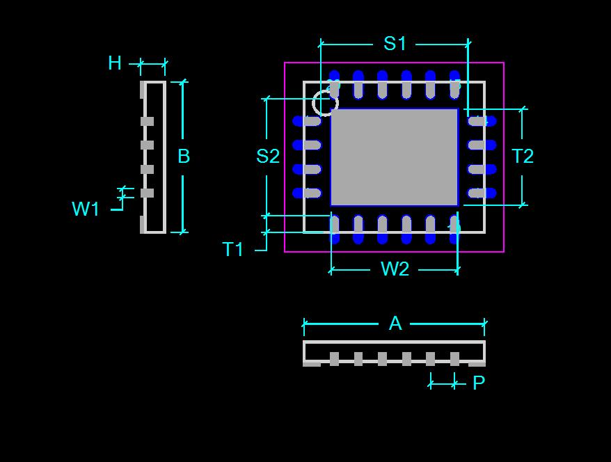
Fig.1 typical dimension of QFN package
Above is the typical dimension specification for QFN package. I cann't find the corresponding "T1" as in Fig.1 in the DRS4 documents, nor any of the tolerance of the dimensions, which are usually expressed in the form of a range between a min. value and a max. value.
So will you specify the dimension of "T1" and "W1", and the dimension tolerance of them?
Thanks and best wishes!
Jinhong Wang University of Science and Technology of China |
|
23
|
Mon Dec 14 10:14:16 2009 |
Jinhong Wang | Trigger of DRS4 | Dear Mr. S. Ritt
The following is my confusion about the trigger of DRS4. It mainly concertrates on the generation of trigger signal to stop DRS4 sampling process for readout of sampled waveform.
As metioned in the datasheet of DRS4, the chip samples the analog input every domino sampling period. After finished sampling a waveform, the sampling process can be stoped by lowering the DWRITE while keeping DENABLE high. But the analog input is asychronous to the Domino CLK. Then, how can we know when to stop the domino sampling process to read out the sampled waveform? Of course, a trigger can be used. But from my present knowledge of DRS4, trigger can only be generated from analog input. Analog input is splited into two channels, one to DRS4 analog input, the other to FPGA as the trigger. However, splitting analog inputs increases the system design complexity, and may lower the total performace. So what is your suggestion?
In our system, there are 8 analog inputs to a signal DRS4 chip, the outputs of DRS4 chip are connected to an 8-channel 14 bit ADC ( AD9252). It wold be kind of you to inform me about the most applicable approach for readout of DRS4 sampled wavefrom.
Best regards.
Sincerely,
Jinhong Wang (wangjinh@mail.ustc.edu.cn) |
|
25
|
Mon Dec 21 10:17:05 2009 |
Jinhong Wang | Trigger of DRS4 |
| Stefan Ritt wrote: |
|
| Jinhong Wang wrote: |
|
Dear Mr. S. Ritt
The following is my confusion about the trigger of DRS4. It mainly concertrates on the generation of trigger signal to stop DRS4 sampling process for readout of sampled waveform.
As metioned in the datasheet of DRS4, the chip samples the analog input every domino sampling period. After finished sampling a waveform, the sampling process can be stoped by lowering the DWRITE while keeping DENABLE high. But the analog input is asychronous to the Domino CLK. Then, how can we know when to stop the domino sampling process to read out the sampled waveform? Of course, a trigger can be used. But from my present knowledge of DRS4, trigger can only be generated from analog input. Analog input is splited into two channels, one to DRS4 analog input, the other to FPGA as the trigger. However, splitting analog inputs increases the system design complexity, and may lower the total performace. So what is your suggestion?
In our system, there are 8 analog inputs to a signal DRS4 chip, the outputs of DRS4 chip are connected to an 8-channel 14 bit ADC ( AD9252). It wold be kind of you to inform me about the most applicable approach for readout of DRS4 sampled wavefrom.
Best regards.
Sincerely,
Jinhong Wang (wangjinh@mail.ustc.edu.cn)
|
Indeed you have to make an external trigger. The evaluation board uses the "transparent mode" of the DRS4 to "mirror" the input signal at the output, then puts a comparator there. The schematics of the evaluation board is in the manual. This does then not degrate the analog performance. You can of course also split the signal at the input, this will only add a minor additional load to the input signal, since the load of the DRS4 chips itself is much bigger than that of any comparator.
An alternative is to turn on the transparent mode and continuously digitize all 8 outputs with your AD9252. Then you make the trigger purely digital in your FPGA. You can put there a comparator, or even more complex logic like multiplicity etc. Note however that this causes some latency, since the ADC has a pipeline which is quite long, so you have to buffer the latency of your trigger in the analog window of the DRS4 sampling cells. Like if you run the DRS4 at 1 GSPS, you can accomodate 1024 ns of sampling depth, which is good for maybe 500 ns of trigger latency plus 500 ns of the waveform of interest.
|
Thank you. The transparent mode can be really helpful. Can you provide me in more details of the chip's transparent mode? I am still confused about the following aspects.
I notice that DRS4 samples the analog wave in the way "clear before write", and in the transparent mode, there will be certain delay before the trigger logic stops the sampling process. So,does it mean that the waveform recording process per Domino sampling cycle will not degrade the amplitude of the analog signal? Hence, for two idential analog inputs, one with a trigger latency of 500 ns and the other of 510 ns, the sampled waveform is identical, what differs is the starting number of the first active sampling cell, where the reading process considered to be started. Is that right? Looking forward to your insight.
Best regrads.
Sincerely,
Jinhong Wang (wangjinh@mail.ustc.edu.cn) |
|
27
|
Tue Dec 22 01:30:55 2009 |
Jinhong Wang | Trigger of DRS4 |
| Stefan Ritt wrote: |
|
| Jinhong Wang wrote: |
|
| Stefan Ritt wrote: |
|
| Jinhong Wang wrote: |
|
Dear Mr. S. Ritt
The following is my confusion about the trigger of DRS4. It mainly concertrates on the generation of trigger signal to stop DRS4 sampling process for readout of sampled waveform.
As metioned in the datasheet of DRS4, the chip samples the analog input every domino sampling period. After finished sampling a waveform, the sampling process can be stoped by lowering the DWRITE while keeping DENABLE high. But the analog input is asychronous to the Domino CLK. Then, how can we know when to stop the domino sampling process to read out the sampled waveform? Of course, a trigger can be used. But from my present knowledge of DRS4, trigger can only be generated from analog input. Analog input is splited into two channels, one to DRS4 analog input, the other to FPGA as the trigger. However, splitting analog inputs increases the system design complexity, and may lower the total performace. So what is your suggestion?
In our system, there are 8 analog inputs to a signal DRS4 chip, the outputs of DRS4 chip are connected to an 8-channel 14 bit ADC ( AD9252). It wold be kind of you to inform me about the most applicable approach for readout of DRS4 sampled wavefrom.
Best regards.
Sincerely,
Jinhong Wang (wangjinh@mail.ustc.edu.cn)
|
Indeed you have to make an external trigger. The evaluation board uses the "transparent mode" of the DRS4 to "mirror" the input signal at the output, then puts a comparator there. The schematics of the evaluation board is in the manual. This does then not degrate the analog performance. You can of course also split the signal at the input, this will only add a minor additional load to the input signal, since the load of the DRS4 chips itself is much bigger than that of any comparator.
An alternative is to turn on the transparent mode and continuously digitize all 8 outputs with your AD9252. Then you make the trigger purely digital in your FPGA. You can put there a comparator, or even more complex logic like multiplicity etc. Note however that this causes some latency, since the ADC has a pipeline which is quite long, so you have to buffer the latency of your trigger in the analog window of the DRS4 sampling cells. Like if you run the DRS4 at 1 GSPS, you can accomodate 1024 ns of sampling depth, which is good for maybe 500 ns of trigger latency plus 500 ns of the waveform of interest.
|
Thank you. The transparent mode can be really helpful. Can you provide me in more details of the chip's transparent mode? I am still confused about the following aspects.
I notice that DRS4 samples the analog wave in the way "clear before write", and in the transparent mode, there will be certain delay before the trigger logic stops the sampling process. So,does it mean that the waveform recording process per Domino sampling cycle will not degrade the amplitude of the analog signal? Hence, for two idential analog inputs, one with a trigger latency of 500 ns and the other of 510 ns, the sampled waveform is identical, what differs is the starting number of the first active sampling cell, where the reading process considered to be started. Is that right? Looking forward to your insight.
Best regrads.
Sincerely,
Jinhong Wang (wangjinh@mail.ustc.edu.cn)
|
The amplitude of the analog signal is not degraded by the transparent mode, since the signal is buffered on the chip, and the output of this buffer is send off the chip. The waveform digitizing of course requires quite some current to charge up all capacitors, so there is maximum current of ~1mA for 5 GSPS. If you only have a weak signal source, your bandwidth might be limited by that. On the evaluation board for example we use passive transformers to produce the differential input signal from a single-ended signal. Although the transformers are rated 1 GHz Bandwidth, we only achieve 200 MHz with the passive transformers. By using active high speed differential drivers, you can get about 700 MHz right now.
If you have two channels with 500 ns and 510 ns trigger latency, there is no difference in the "domino stop position" since there is only one domino circuit per chip which can be stopped. So the stop position is the same for all eight channels on a chip.
|
So you mean there is an analog buffer per channel? The analog signal is buffered there, before entering the sampling cells? Then, when will the buffer content be released and cleared? How shall I handle "Dwite" and "Denable" during a complete operation when an analog signal arrives in the transparent mode? I cannot find more information beyond the datasheet, a detailed description of the transparent mode (and the analog buffer, if possible) will be really helpful for me.
Best,
Sincerely,
Jinhong Wang (wangjinh@mail.ustc.edu.cn) |
|