| ID |
Date |
Author |
Subject |
|
584
|
Sat Jan 28 14:11:58 2017 |
Danny Petschke | AND trigger problems | Dear Stefan,
I have 2 identical pulses as a splittet signal with an amplitude of 300mV. Range is -0.5-0.5V, 5.12GSamp using the Evaluation-Board. Both signals are triggered in AND logic. One of the signals is delayed by a fixed value of 1-50ns for testing. On increasing the trigger Level from 10% to 50% of amplitude (pulse rise time is 2.5ns) pulses cannot anymore triggered above 4-5ns delay. It means there is a proportionality between the trigger level and the available range where 2 signals can be triggered in AND logic (Time-difference between 2 pulses). Do I anything misunderstand or is the time the comparator needs by higher trigger Levels for comparation longer than the 200ns at 5.12GSamp?
Board was timing and voltage calibrated before.
Thx
Danny |
|
400
|
Thu Mar 19 07:37:52 2015 |
Daniel Stricker-Shaver | Running 2 instances of a DRS DAQ program | I don't know if it helps, but we measured the time resolution between two independendly running v3 boards using a single PC (latest software) in Linux. (http://arxiv.org/abs/1405.4975)
You start the DRS DAQ program with only one USB board connected, first. Afterwards connect the second board and start another session. If you externally trigger (global) both boards with less than 1 Hz, you can garantee that both programs save the same events independently (from two individual DRS boards).
Daniel
| Stefan Ritt wrote: |
|
I never had in mind running two systems in parallel, that's why the code claims all interfaces when started. You have to dig into the usb code which is located in musbstd.c at function musb_open(). There you will find a line libusb_claim_interface() which requests exclusive access to the usb subsystem. The code is there because I copied it from some standard example for the libusb library. You have to read the documentation for libusb (http://libusb.sourceforge.net/api-1.0/) and see if you can get rid of that. Probaby you have to claim/release the interface on each access, but I never tried that.
Stefan
| Hermann-Josef Mathes wrote: |
|
Hi,
we want to run two instances of our little DRS DAQ program but obviously the first instance started always claims all DRS boards for itself and the other one exits with an error. The 2 boards used in the example below have the serial number # 2413 and #2414 and are v5 boards.
The first one:
mathes@ikauger5:~/src/DRS4/Cpp> ./drsdaq -b 2413
DRSController: found board with serial number #2413
DRSController: found board with serial number #2414
DRSController: using board with serial number #2413
CalibratedFrequency= 1.00721
====================================
DRS type: DRS4
Board type: 9
Serial number: 2413
Firmware revision: 21260
...
And the second one:
mathes@ikauger5:~/src/DRS4/Cpp> ./drsdaq -b 2414
musb_open: usb_set_configuration() error -6
musb_open: Found USB device 0x04b4:0x1175 instance 0, but cannot initialize it: please check permissions on "/proc/bus/usb/1/7" and "/dev/bus/usb/1/7"
USB successfully scanned, but no boards found
...
How can our goal be achieved?
Thanks
Hermann-Josef
|
|
|
|
407
|
Tue Apr 21 13:03:38 2015 |
Daniel Stricker-Shaver | DRS4 Evaluation Board Baseline/Voltage Calibration | I also use Ubuntu 14.04 LTS and for my V3 borad I have to use drsosc 4.x or ealier to perform the calibration.
| Stefan Ritt wrote: |
|
1) I tried to cablirate a V5 board with drsosc 5.0.3 and it just worked fine for me. No idea what went wrong in your case.
2) The "found 4096 stuck pixels on this board" can be safely ignored. It comes from the fact that the standard evaluation board has four cannels unconnected (the DRS4 chip has 8 channels, four are connected to in the evaluation board and four are unconnected). So the software sees wrong values on four channels because they are unconnected and thinks something is wrong. Unfortunately the software cannot determine if the channels are connected or not. So just ignore it.
3) I heard several people having to reset their boards under Linux in a similar way than you. This is probalby due to some instability in the USB part of the linux kernel, since the problem does not occur on other systems (Windows, Mac OSX). So I cannot do anything from the software side.
/Stefan
| Julien Wulf wrote: |
|
Hi,
I`m trying to calibrate my DRS4 evoluation board to an input range of 0-1V but it doesn`t work.
1) First I tried to calibrate it with the drsosc (version 5.0.3) Software. The -0.5V - 0.5V calibration works, but during the 0 - 1V calibration the Software crashes.
2) I also tried to calibrate the input range with a C++ DAQ Package (based on drs_exam). Here the code of the calibration:
....
b->SetInputRange(0.) (Center at 0 V )
b->CalibrateVolt(NULL);
....
Calibration Works
....
b->SetInputRange(0.5) (Center at 0.5 V )
b->CalibrateVolt(NULL);
....
Results in: Found 4096 stuck pixels on this board.
Did I do a mistake or is this a normal behaviour of the board? Also the board often crashes and I get a magic number 0000 after restarting the DAQ. Then the board needs to be restarted via pulling the plug. ( I ensured that I terminate the USB connection before I close the program with "delete drs"). Is there a possibility to avoid this error?
My OS: Ubuntu 14.04 LTS.
Ciao,
Julien
|
|
|
|
511
|
Sat Apr 23 12:33:17 2016 |
Daniel Stricker-Shaver | Negative fCellDT values from GetTimeCalibration() | Hi Kyle,
If I remember right the negative sampling width happens only for 498 and at high sampling speeds. It is described in a paper from Stefan:
http://arxiv.org/pdf/1405.4975.pdf
or
“Novel Calibration Method for Switched Capacitor Arrays Enables Time Measurements With Sub-Picosecond Resolution”( IEEE Transactions on Nuclear Science 61 (2014),Nr. 6, 3607–3617)
| Kyle Weinfurther wrote: |
|
Hello Stefan,
I am using four DRS4 v5 eval boards to digitize 16 channels of data. I have recently changed from saving the timing information of the waveform using GetTime() to GetTimeCalibration(). When changing over, I noticed that some values for fCellDT for cell 498 are negative. Over the 16 channels used, 4 of them have negative time bin widths for cell 498 while the other 12 channels are very close to 0 (in the ~10 ps range). One of the eval boards has no negative fCellDT whereas the other three boards have one or two channels with negative values.
Upon further inspection, I checked the time between samples of GetTime() and found the same results in cell 498. After finding this, I did a timing calibration again with CalibrateTiming() even though in a different post on the discussion forum you said it was valid for a wide range of temperatures and a long time (years). This still allowed the negative fCellDT values to persist.
Is this a common occurance? If so, is there a method to fix this issue? Is there a reason for cell 498 to have a small value for fCellDT? I searched the discussion forum and did not find anything relating to this issue.
Attached are a couple waveform traces using GetTime() zoomed in on cell 498.
Thanks,
Kyle Weinfurther
|
|
|
485
|
Mon Mar 21 10:38:27 2016 |
Daniel Dribin | DRS Oscilloscope freezing after a long run | Dear Stefan Ritt,
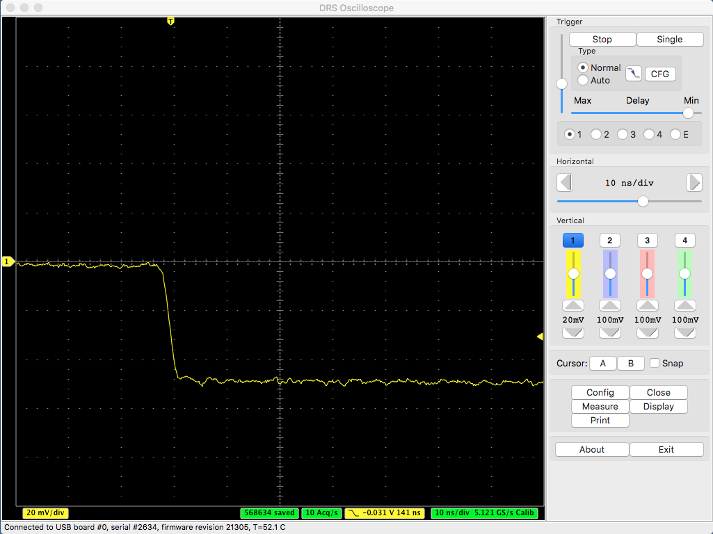
I am using a DRS4 v5 to do timing measurements of Positron lifetime. I use the DRS Oscilloscope with triggering on 2 channels when I have a coincidence. Attached is a picture with all the setting that I use. When I use the DRS4 for a long measurements of 5 million events for a couple of hours, the DRS Oscilloscope stops showing any signal .After the first restart of the program I get a strange signal which is at the bottom of the scope range of voltage picture below(in the picture I changed the vertical positions of the channels for better viewing). Only after a couple of DRS Oscilloscope restarts and USB reconnections do I get the results again.
I currently am using another DRS4 v5 and the same situation occurs again although with lower frequency.
What can I do to solve this problem?
thank you very much,
Daniel
|
| Attachment 1: drs_settings.png
|

|
| Attachment 2: empty_drs.png
|

|
| Attachment 3: drs_ofset.png
|

|
|
501
|
Mon Apr 4 11:41:26 2016 |
Daniel Dribin | DRS Oscilloscope freezing after a long run | Dear Stefan Ritt,
Yes I use Windows 7, If the DRS Oscilloscope program stays on for a couple of hours without saving the data, the problem will occur. It seems it happens more often when there is data writing and when the rate of events is slow, about 100 events per second, at high rates it almost doesn't happen. Can it be temperature related?
Daniel
| Stefan Ritt wrote: |
|
Dear Daniel,
sorry my late reply, I'm pretty busy these days. The behavior you report has not been seen before, but I guess no one tried to take such long runs of data yet. Can you confirm that the problem also occurs without writing data to disk, or is it disk-related? I guess you use it under Windows 7, right?
Stefan
| Daniel Dribin wrote: |
|
Dear Stefan Ritt,
I am using a DRS4 v5 to do timing measurements of Positron lifetime. I use the DRS Oscilloscope with triggering on 2 channels when I have a coincidence. Attached is a picture with all the setting that I use. When I use the DRS4 for a long measurements of 5 million events for a couple of hours, the DRS Oscilloscope stops showing any signal .After the first restart of the program I get a strange signal which is at the bottom of the scope range of voltage picture below(in the picture I changed the vertical positions of the channels for better viewing). Only after a couple of DRS Oscilloscope restarts and USB reconnections do I get the results again.
I currently am using another DRS4 v5 and the same situation occurs again although with lower frequency.
What can I do to solve this problem?
thank you very much,
Daniel
|
|
|
|
506
|
Wed Apr 6 09:43:52 2016 |
Daniel Dribin | DRS Oscilloscope freezing after a long run | At hight rates I worked with files of up to 20 GB so I don't think this is the problem.
I will try to run it under Ubuntu and see if i can recreate the problem.
Thank you very much for the quick responses and help.
| Stefan Ritt wrote: |
|
Even with writing for one night no problem (see below). Have you checked how big your data file is? I guess there is a limit under Windows of 2 GB. If that's the case, you have to write shorter files.
|
|
|
507
|
Wed Apr 6 09:46:10 2016 |
Daniel Dribin | DRS Oscilloscope freezing after a long run |
| Martin Petriska wrote: |
|
| Stefan Ritt wrote: |
|
I tried this night to run the board at a 10 Hz rate with an external pulser, without writing, and it did not freeze after ~14 hours of running on Mac OSX. This night I will try again with writing.
Stefan
| Stefan Ritt wrote: |
|
Then it seems that there is some USB communication problem. I heard this also from other people, that the USB data transfer under Windows has sometimes problems. I develop and run the board under Mac OSX, and there the same software runs for days without problem. So I guess it's related to the underlying libusb lib which is used by the DRS oscilloscope, on which I have no influence. So the only advice I can give is to take shorter series of data. Anyhow the board is not considered a full DAQ system, just an "evaluation board" which means one can try the DRS4 chip and play with it. For serious business one should build own electronics with the chip. Anyhow we are currently developping an Ethernet board which allows much faster acquisition rates, so USB will be obsolete some day. Nevertheless I will try to reproduce your problem and see if I can do anything. At what trigger rate does it show up most prominently?
Stefan
| Daniel Dribin wrote: |
|
Dear Stefan Ritt,
Yes I use Windows 7, If the DRS Oscilloscope program stays on for a couple of hours without saving the data, the problem will occur. It seems it happens more often when there is data writing and when the rate of events is slow, about 100 events per second, at high rates it almost doesn't happen. Can it be temperature related?
Daniel
| Stefan Ritt wrote: |
|
Dear Daniel,
sorry my late reply, I'm pretty busy these days. The behavior you report has not been seen before, but I guess no one tried to take such long runs of data yet. Can you confirm that the problem also occurs without writing data to disk, or is it disk-related? I guess you use it under Windows 7, right?
Stefan
| Daniel Dribin wrote: |
|
Dear Stefan Ritt,
I am using a DRS4 v5 to do timing measurements of Positron lifetime. I use the DRS Oscilloscope with triggering on 2 channels when I have a coincidence. Attached is a picture with all the setting that I use. When I use the DRS4 for a long measurements of 5 million events for a couple of hours, the DRS Oscilloscope stops showing any signal .After the first restart of the program I get a strange signal which is at the bottom of the scope range of voltage picture below(in the picture I changed the vertical positions of the channels for better viewing). Only after a couple of DRS Oscilloscope restarts and USB reconnections do I get the results again.
I currently am using another DRS4 v5 and the same situation occurs again although with lower frequency.
What can I do to solve this problem?
thank you very much,
Daniel
|
|
|
|
|
Hi I have also positron annihilation system based on DRS4v4 cards. Its running several weeks, sometimes months, without freezing in windows7 64bit system (Pentium Core Quad 2Ghz, 4GRam). Problem was when widows was trying to install updates and restarted PC. In beginning I had some problem with memory leak in my application, but it was simple seen in task manager that application memory was rising and was need to find memory leak in application code. Now I remember card was sometimes freezing when room air conditioning with 2kW was starting and high electricity pulses were reason of USB problems, it helped to put air conditioner and PC in different power line input. Hope it help to solve zour problems.
Martin
|
I too have air conditioning in the room, not sure to which power line it is connected, but I'll try to check this aswell.
Thank you very much. |
|
409
|
Wed May 13 00:52:51 2015 |
Cosmin Deaconu | Getting Trigger Source | I'd like to be able to know which channel (0,1,2,3 or external) was responsible for the trigger. DRSBoard::GetTriggerSource() seems to always return 1. Is there a way to get this information? Using the DRS4 evaluation board and software version 5.0.3.
Thanks,
Cosmin
|
|
410
|
Wed May 13 01:07:36 2015 |
Cosmin Deaconu | DRS4 Evaluation Board + Powered USB Hub | I am trying to use 4 evaluation boards with a powered USB hub (since eventually, I will have to do this on a laptop). It seems like destroying the DRS object is insufficent to properly close the boards when on the hub (i.e. I get usb read errors next time I run my program). When all the boards are plugged into the computer, all is fine. This is on Linux using libusb1. My guess is something about resetting the port doesn't work properly (but maybe that's this particular hub's fault?). Has anyone else experienced a similar issue. If not, can someone recommend a hub that is known to work? |
|
553
|
Fri Nov 4 17:41:03 2016 |
Christian Farina | Missing Header | Hello everybody,
I am completely new to this, so please bear with me.
I am trying to install the applications on my laptop. I downloaded and untar-ed the drivers and applications for Linux as described in the evaluation board manual. However, when I do the make, I get the following error:
drs-4.0.0$ make
g++ -g -O2 -Wall -Wuninitialized -fno-strict-aliasing -Iinclude -DOS_LINUX -DHAVE_LIBUSB -DUSE_DRS_MUTEX -c src/musbstd.c
In file included from src/musbstd.c:14:0:
include/musbstd.h:17:17: fatal error: usb.h: No such file or directory
#include <usb.h>
Can anybody help me please?
Thanks. |
|
555
|
Wed Nov 9 17:19:48 2016 |
Christian Farina | Missing Header | Thank you Stefan, that was just what I needed.
Also, I have another question, if I am allowed to ask on this forum. I am trying to study how the time calibration of the DRS is done. Can you point me to the script in which this is done?
Thank you,
Christian
| Stefan Ritt wrote: |
|
The web page from where you downloaded the software contains a sentence "requires libusb-1.0 package". Please install it. This package brings the "usb.h" header file.
Stefan
| Christian Farina wrote: |
|
Hello everybody,
I am completely new to this, so please bear with me.
I am trying to install the applications on my laptop. I downloaded and untar-ed the drivers and applications for Linux as described in the evaluation board manual. However, when I do the make, I get the following error:
drs-4.0.0$ make
g++ -g -O2 -Wall -Wuninitialized -fno-strict-aliasing -Iinclude -DOS_LINUX -DHAVE_LIBUSB -DUSE_DRS_MUTEX -c src/musbstd.c
In file included from src/musbstd.c:14:0:
include/musbstd.h:17:17: fatal error: usb.h: No such file or directory
#include <usb.h>
Can anybody help me please?
Thanks.
|
|
|
|
561
|
Thu Nov 10 20:54:45 2016 |
Christian Farina | Missing Header | Hi Stefan,
I have already read the paper. I was just unsure where the calibration code was located. Thank you so much for all your help.
Christian
| Stefan Ritt wrote: |
|
Best is to read this paper: https://arxiv.org/abs/1405.4975
The source code for that is in DRS.cpp in the DRS software distribution in the function DRSBoard::CalibrateTiming()
Stefan
| Christian Farina wrote: |
|
Thank you Stefan, that was just what I needed.
Also, I have another question, if I am allowed to ask on this forum. I am trying to study how the time calibration of the DRS is done. Can you point me to the script in which this is done?
Thank you,
Christian
| Stefan Ritt wrote: |
|
The web page from where you downloaded the software contains a sentence "requires libusb-1.0 package". Please install it. This package brings the "usb.h" header file.
Stefan
| Christian Farina wrote: |
|
Hello everybody,
I am completely new to this, so please bear with me.
I am trying to install the applications on my laptop. I downloaded and untar-ed the drivers and applications for Linux as described in the evaluation board manual. However, when I do the make, I get the following error:
drs-4.0.0$ make
g++ -g -O2 -Wall -Wuninitialized -fno-strict-aliasing -Iinclude -DOS_LINUX -DHAVE_LIBUSB -DUSE_DRS_MUTEX -c src/musbstd.c
In file included from src/musbstd.c:14:0:
include/musbstd.h:17:17: fatal error: usb.h: No such file or directory
#include <usb.h>
Can anybody help me please?
Thanks.
|
|
|
|
|
|
600
|
Thu Apr 13 16:42:21 2017 |
Christian Farina | Stand-alone Time Calibration for PSI Board | Hello everybody,
I was trying to create a stand-alone program that would perform a time calibration on the board. My goal would be the following.
- acquire about 10k sinus waveforms
- write them to disk (also for later reanalysis)
- run the time calibration on the recorded data
- store the clibration results in a file / database
Being not an expert, my question here is the following. Would it be easier to try to isolate the time calibration part from the DRS.cpp source code or re-write entirely the code from scratch?
Thanks. |
|
602
|
Thu Apr 13 16:54:32 2017 |
Christian Farina | Stand-alone Time Calibration for PSI Board | Hi Stefan,
Thank you for your reply. I have read the paper already. I looked through the code and I understand that the LTC and GTC are performed by the AnalyzeSlope and AnalyzePeriod functions, respectively, correct? It seems to me to be a complicated business to re-write that part from scratch, at least for an inexperienced programmer like me. It made more sense to try to isolate that part from the original DRS.cpp. Ideally, I would like to have a stand-alone program that would work on any SCA without references to the drs hardware specifics.
| Stefan Ritt wrote: |
|
Hard to say. Timing calibration is quite delicate. If you start from scratch, better read this paper: https://arxiv.org/abs/1405.4975
If you try to extract the code from DRS.cpp, better read the paper, too. Probably it will not be possible to develop or extract the code without knowing how it works.
Best,
Stefan
| Christian Farina wrote: |
|
Hello everybody,
I was trying to create a stand-alone program that would perform a time calibration on the board. My goal would be the following.
- acquire about 10k sinus waveforms
- write them to disk (also for later reanalysis)
- run the time calibration on the recorded data
- store the clibration results in a file / database
Being not an expert, my question here is the following. Would it be easier to try to isolate the time calibration part from the DRS.cpp source code or re-write entirely the code from scratch?
Thanks.
|
|
|
|
604
|
Thu Apr 13 17:10:58 2017 |
Christian Farina | Stand-alone Time Calibration for PSI Board | Thank you for your help Stefan. I will try to get the TC part isolated.
| Stefan Ritt wrote: |
|
Than you can try to isolate the code. Note that different SCAs might work differently. Like the DRS4 has a channel-to-channel jitter which others might not. But you will see.
Stefan
| Christian Farina wrote: |
|
Hi Stefan,
Thank you for your reply. I have read the paper already. I looked through the code and I understand that the LTC and GTC are performed by the AnalyzeSlope and AnalyzePeriod functions, respectively, correct? It seems to me to be a complicated business to re-write that part from scratch, at least for an inexperienced programmer like me. It made more sense to try to isolate that part from the original DRS.cpp. Ideally, I would like to have a stand-alone program that would work on any SCA without references to the drs hardware specifics.
| Stefan Ritt wrote: |
|
Hard to say. Timing calibration is quite delicate. If you start from scratch, better read this paper: https://arxiv.org/abs/1405.4975
If you try to extract the code from DRS.cpp, better read the paper, too. Probably it will not be possible to develop or extract the code without knowing how it works.
Best,
Stefan
| Christian Farina wrote: |
|
Hello everybody,
I was trying to create a stand-alone program that would perform a time calibration on the board. My goal would be the following.
- acquire about 10k sinus waveforms
- write them to disk (also for later reanalysis)
- run the time calibration on the recorded data
- store the clibration results in a file / database
Being not an expert, my question here is the following. Would it be easier to try to isolate the time calibration part from the DRS.cpp source code or re-write entirely the code from scratch?
Thanks.
|
|
|
|
|
|
483
|
Wed Mar 9 09:57:20 2016 |
Christian D | LabView | Hi,
I would like to use the DRS4 board with LabView for fast readout.
Do you know anyone who has written a VI for that?
Thanks,
Christian |
|
392
|
Sun Oct 19 14:36:54 2014 |
Chris Tully | coverting the xml file format into binary | Hi,
Is there a straightforward way to convert the xml file format into the binary format? I have some runs taken mistakenly with xml.
Best,
Chris
|
|
451
|
Wed Nov 25 02:52:35 2015 |
Chris Thompson | PC software beyond Windows 7 | I am new to this forum. I have ordered a DRS4 evaluation board for doing experiments with very fast PET detectors. It has not arrived yet. The version of the manual I downloaded today shows software installation instructions for Windows 7 and earlier versions. I intend to use it on a 64bit PC running Windows 8.1. Will the Windows 7 driver work, or is there an updated version for Windows 8 or 10? |
|
453
|
Wed Nov 25 17:36:25 2015 |
Chris Thompson | PC software beyond Windows 7 | I tried this suggestion of changing the startup settings to ingore driver license signing (as suggested in the post # 434), but when I tried to install the software I got a error message which I captured from the screen and I have attached. Perhaps I have the wrong version, or, as suggested, the file I downloaded from your site is incomplete?
| Stefan Ritt wrote: |
|
Have a look here elog:434
| Chris Thompson wrote: |
|
I am new to this forum. I have ordered a DRS4 evaluation board for doing experiments with very fast PET detectors. It has not arrived yet. The version of the manual I downloaded today shows software installation instructions for Windows 7 and earlier versions. I intend to use it on a 64bit PC running Windows 8.1. Will the Windows 7 driver work, or is there an updated version for Windows 8 or 10?
|
|
|
| Attachment 1: Installation_failure_screen.jpg
|

|
|