| ID |
Date |
Author |
Subject |
|
455
|
Sat Dec 5 02:39:20 2015 |
Chris Thompson | PC software beyond Windows 7 | I tried restarting Windows 10 in a way the allowed me to use "advanced startup options" Option 7 suggested it was to restart without mandatory driver signing. However, the error persists. Has anyone tested this latest version 5.0.4 on Windows 10? My hardware arrived today, and I am anxious to test it.!!!!
| Chris Thompson wrote: |
|
I tried this suggestion of changing the startup settings to ingore driver license signing (as suggested in the post # 434), but when I tried to install the software I got a error message which I captured from the screen and I have attached. Perhaps I have the wrong version, or, as suggested, the file I downloaded from your site is incomplete?
| Stefan Ritt wrote: |
|
Have a look here elog:434
| Chris Thompson wrote: |
|
I am new to this forum. I have ordered a DRS4 evaluation board for doing experiments with very fast PET detectors. It has not arrived yet. The version of the manual I downloaded today shows software installation instructions for Windows 7 and earlier versions. I intend to use it on a 64bit PC running Windows 8.1. Will the Windows 7 driver work, or is there an updated version for Windows 8 or 10?
|
|
|
|
|
456
|
Sat Dec 5 03:21:21 2015 |
Chris Thompson | PC software beyond Windows 7 | On a hunch, I tried downloading V 5.0.3 instead. This works, and I now have the oscilloscope mode displaying signals! (just to make sure, I re-tire version 5.0.4 and still get the same error. So, in summary V 5.0.3 seems to install successfully and work with Windows 10, but the newer V5.0.4 does not install... I assmume that I am missing something though, as the newer version is 10 Mbytes bigger!
| Chris Thompson wrote: |
|
I tried restarting Windows 10 in a way the allowed me to use "advanced startup options" Option 7 suggested it was to restart without mandatory driver signing. However, the error persists. Has anyone tested this latest version 5.0.4 on Windows 10? My hardware arrived today, and I am anxious to test it.!!!!
| Chris Thompson wrote: |
|
I tried this suggestion of changing the startup settings to ingore driver license signing (as suggested in the post # 434), but when I tried to install the software I got a error message which I captured from the screen and I have attached. Perhaps I have the wrong version, or, as suggested, the file I downloaded from your site is incomplete?
| Stefan Ritt wrote: |
|
Have a look here elog:434
| Chris Thompson wrote: |
|
I am new to this forum. I have ordered a DRS4 evaluation board for doing experiments with very fast PET detectors. It has not arrived yet. The version of the manual I downloaded today shows software installation instructions for Windows 7 and earlier versions. I intend to use it on a 64bit PC running Windows 8.1. Will the Windows 7 driver work, or is there an updated version for Windows 8 or 10?
|
|
|
|
|
|
475
|
Thu Jan 14 21:49:37 2016 |
Chris Thompson | Triggering of DRS4 in the fastest sampling mode | I am attempting to use the DRS4 to measure the timing resolution of a pair of SensL silicon photomultipliers (SiPM). In order to do this I need to trigger the DRS4 only when there is a coincidence between the two input signals, and hopefully make histograms of the relative detection times of each detector.
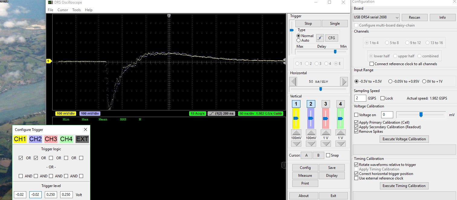
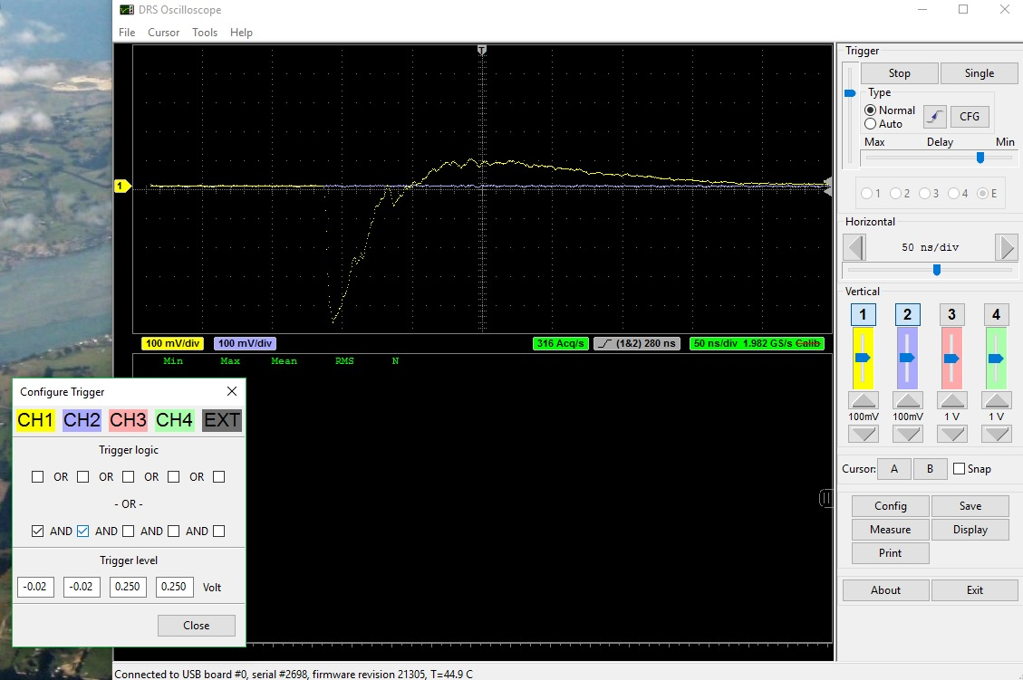
There are two completely separate issues. (1) I think this may just be a labelling error. In the first image (OR_mode_selected) one can clearly see two pulses which are very similar. In this mode, both signals are present, and are always present. I think this should be the "AND", not "OR" of the two signals. Contrast this with the second image where I have selected "AND_mode". Clearly only one signal is present, and either signal trigges an event, so this should be "OR", not "AND"
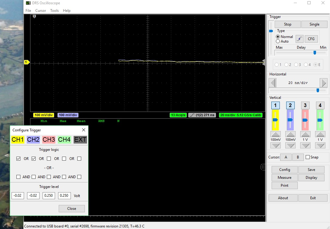
The second issue is, for me, much more serious. I want to sample the leading edge of this event in order to determine its "time". The little "T" at the top of each image is, I believe the "trigger point" in the first two images. However, this is well after the part of the signal I am interested in. The first two images were at 2 GigaSamples/sec. The third is at 5 GigaSamples/sec. Clearly the event I am interested in processing is over by then. At the lower sampling rate, I can see well before the "T", but at the higher one I can only see after the "T". I had built an external "coincidence circuit" and the "external trigger mode" hoping to to circumvent this issue by using very long cables to delay the signals inut to the DRS4, But even then I have not been successful in getting the to work.
I am using version 5.0.3 on a PC as the version released after that did not work.
I hope some can help!
Chris Thompson |
| Attachment 1: OR_mode_selected.jpg
|
|
| Attachment 2: AND_mode_selected.jpg
|
|
| Attachment 3: 20ns_per_div.jpg
|
|
|
492
|
Thu Mar 31 20:48:00 2016 |
Chris Thompson | Trigger on the And of a positive and negative signal | I needed a fast pulse inverter in order to feed signals from the recent SensL SiPMs into a conventional CFD which only accepted negative signals. I got a very small ferite torridal transformer from Coilcraft and wired up to invert signals then inserted into in 50 ohm coax cable and it works fine. These things cost only a few cents each!
| Abaz Kryemadhi wrote: |
|
Thanks, that looks just fine.
| Stefan Ritt wrote: |
|
Here is one (SI 100): https://www.picoquant.com/products/category/accessories/adapters-splitters-cables-various-accessories-for-photon-counting-setups
| Abaz Kryemadhi wrote: |
|
Ok, thanks! do you know an easy in-line inverter like mini-circuit or digikey? Can also redesign the detector I gues to produce positive signals, just it might be easier if there was a simple inverter if you are aware of? thanks Abaz
| Stefan Ritt wrote: |
|
No. You have to use an inverter for one of your signals.
Stefan
| Abaz Kryemadhi wrote: |
|
I would like to be able to trigger in this fashon: channel 0 > 0.1 and. channel 1< -0.1, because I have a positive and a negative signal. Can DRS4 (5) Eval board do this kind of trigger?
Thanks!
Abaz
|
|
|
|
|
|
|
494
|
Fri Apr 1 22:09:07 2016 |
Chris Thompson | Trigger on the And of a positive and negative signal | The coilcraft part number is: JA4220-ALB. Iordered two of them and they were sent as free samples. You might want to buy some slightly bigger ones. I found them so small it was very hard to solder the coax cable to the connectors. Since I got them, I managed to damage one as they are quite fragile! In the confirmation email I got there was some contact info which may be useful for you: "For help, contact Victoria Berner at 847-516-5551 vberner@coilcraft.com " BTW every time I use this forum I'm told that my password is not valid. Each time I reset it according to the "Lost pasword preceedure. Then I can log on again. Its quite annoying.
| Abaz Kryemadhi wrote: |
|
Hi Chris,
I am looking at Sensl SiPMs as well, can you send the part number from Coilcraft?
Thanks!
Abaz
| Chris Thompson wrote: |
|
I needed a fast pulse inverter in order to feed signals from the recent SensL SiPMs into a conventional CFD which only accepted negative signals. I got a very small ferite torridal transformer from Coilcraft and wired up to invert signals then inserted into in 50 ohm coax cable and it works fine. These things cost only a few cents each!
| Abaz Kryemadhi wrote: |
|
Thanks, that looks just fine.
| Stefan Ritt wrote: |
|
Here is one (SI 100): https://www.picoquant.com/products/category/accessories/adapters-splitters-cables-various-accessories-for-photon-counting-setups
| Abaz Kryemadhi wrote: |
|
Ok, thanks! do you know an easy in-line inverter like mini-circuit or digikey? Can also redesign the detector I gues to produce positive signals, just it might be easier if there was a simple inverter if you are aware of? thanks Abaz
| Stefan Ritt wrote: |
|
No. You have to use an inverter for one of your signals.
Stefan
| Abaz Kryemadhi wrote: |
|
I would like to be able to trigger in this fashon: channel 0 > 0.1 and. channel 1< -0.1, because I have a positive and a negative signal. Can DRS4 (5) Eval board do this kind of trigger?
Thanks!
Abaz
|
|
|
|
|
|
|
|
|
498
|
Sun Apr 3 22:10:19 2016 |
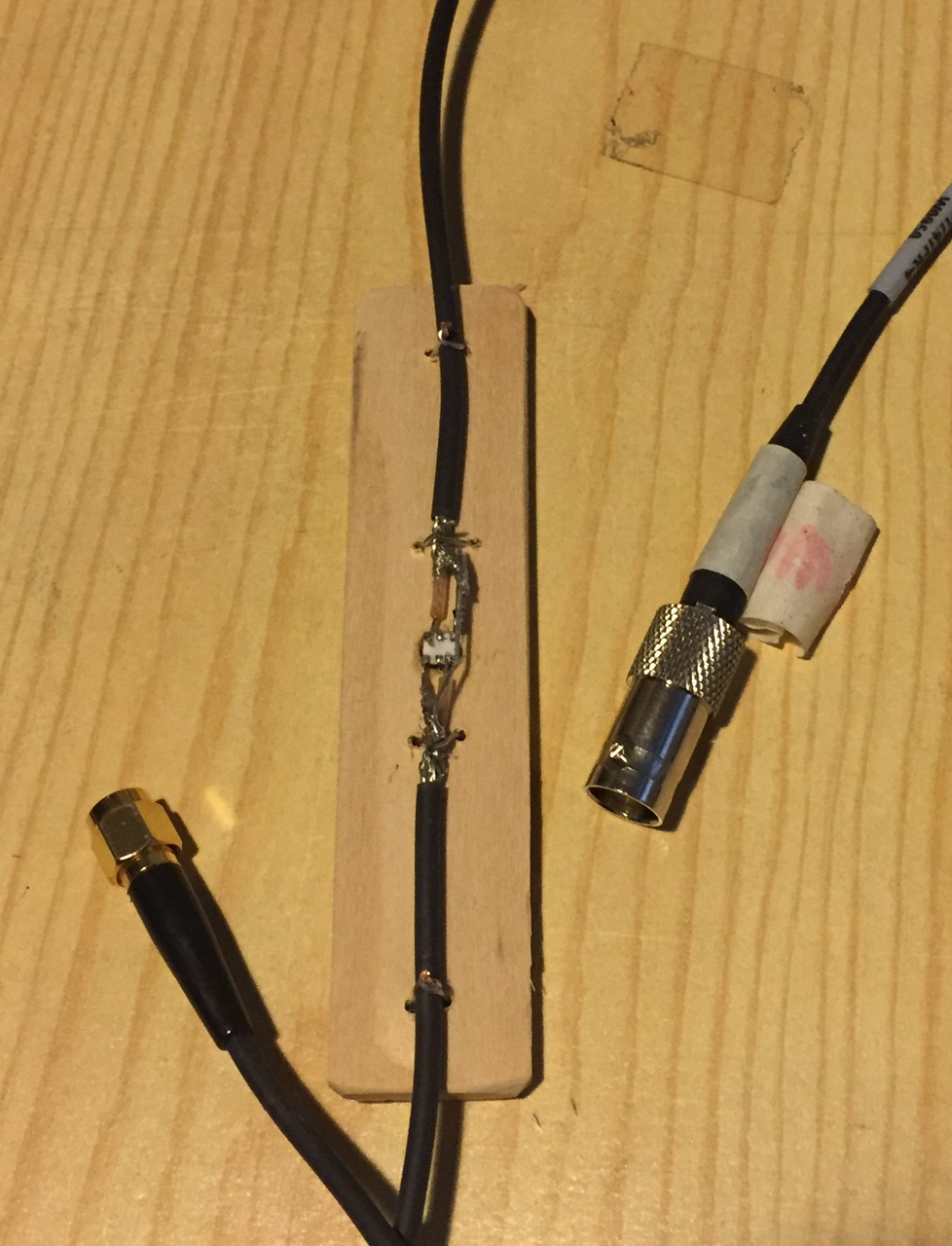
Chris Thompson | Trigger on the And of a positive and negative signal | No there are no other components. I put a photo of the inverter with its cables SMA and one end, BNC at the other. You can see it is very small. I glued the inverter to a piece of thin plywood, and fixed the cables to it before attempting to solder them to the pads on the ferite bead support
| Abaz Kryemadhi wrote: |
|
Thanks again, this is very useful, just another question did you put any other passive elements in the circuit for inverting the signal or just simply swaped the transformer connections?
| Chris Thompson wrote: |
|
The coilcraft part number is: JA4220-ALB. Iordered two of them and they were sent as free samples. You might want to buy some slightly bigger ones. I found them so small it was very hard to solder the coax cable to the connectors. Since I got them, I managed to damage one as they are quite fragile! In the confirmation email I got there was some contact info which may be useful for you: "For help, contact Victoria Berner at 847-516-5551 vberner@coilcraft.com " BTW every time I use this forum I'm told that my password is not valid. Each time I reset it according to the "Lost pasword preceedure. Then I can log on again. Its quite annoying.
| Abaz Kryemadhi wrote: |
|
Hi Chris,
I am looking at Sensl SiPMs as well, can you send the part number from Coilcraft?
Thanks!
Abaz
| Chris Thompson wrote: |
|
I needed a fast pulse inverter in order to feed signals from the recent SensL SiPMs into a conventional CFD which only accepted negative signals. I got a very small ferite torridal transformer from Coilcraft and wired up to invert signals then inserted into in 50 ohm coax cable and it works fine. These things cost only a few cents each!
| Abaz Kryemadhi wrote: |
|
Thanks, that looks just fine.
| Stefan Ritt wrote: |
|
Here is one (SI 100): https://www.picoquant.com/products/category/accessories/adapters-splitters-cables-various-accessories-for-photon-counting-setups
| Abaz Kryemadhi wrote: |
|
Ok, thanks! do you know an easy in-line inverter like mini-circuit or digikey? Can also redesign the detector I gues to produce positive signals, just it might be easier if there was a simple inverter if you are aware of? thanks Abaz
| Stefan Ritt wrote: |
|
No. You have to use an inverter for one of your signals.
Stefan
| Abaz Kryemadhi wrote: |
|
I would like to be able to trigger in this fashon: channel 0 > 0.1 and. channel 1< -0.1, because I have a positive and a negative signal. Can DRS4 (5) Eval board do this kind of trigger?
Thanks!
Abaz
|
|
|
|
|
|
|
|
|
|
| Attachment 1: Pulse_inverter.jpg
|
|
|
357
|
Fri Jun 27 11:23:19 2014 |
ChengMing Du | drsosc binary to cern ROOT file conversion |
| Stefan Ritt wrote: |
|
| Luka Pavelic wrote: |
|
Thank you for your fast and very helpful replay.
I made it work with drsosc version 4 but with version 5 i am getting weird results. Is it possible that they changed binary formatting?
|
Yes, but this is documented in the evaluation board manual. You have to modify the script slightly. I will update it myself in about 2-3 weeks.
Cheers,
Stefan
|
hi Stefan,can you update the code to convert binary to root for newest drsosc?Thanks. |
|
412
|
Wed May 13 09:31:18 2015 |
Chenfei Yang | transparent-mode voltage | Hello Mr. Stefan Ritt
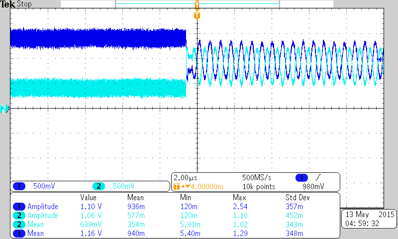
For DRS4 differential inputs ranges form 500mV to 1100mV, with ROFS set to 1.55V, O_OFS set to 1.3V, the outputs of DRS4 is shown in the attachment.
The left part of the waveform,DRS4 works in transparent mode, and then the readout take place. The DMV of transparent mode is bigger then the readout mode, and that makes ADC sampling harder.How may I solve this problem?
Best wishes!
Chenfei Yang |
| Attachment 1: tek00000_.png
|
|
|
414
|
Wed May 13 09:55:09 2015 |
Chenfei Yang | transparent-mode voltage | Here's the problem. My external ADC has 2Vpp differtial input voltage range. And the common-mode voltage of the inputs need to be 1.3V. I cannot make both the transparent-output and the readout-output meet the ADC input requirement.
| Stefan Ritt wrote: |
|
The ROFS signal has no effect in the transparent mode, so you have to adjust O_OFS between sampling and transparent mode accordingly. Either use a DAC or two voltages with an analog switch.
| Chenfei Yang wrote: |
|
Hello Mr. Stefan Ritt
For DRS4 differential inputs ranges form 500mV to 1100mV, with ROFS set to 1.55V, O_OFS set to 1.3V, the outputs of DRS4 is shown in the attachment.
The left part of the waveform,DRS4 works in transparent mode, and then the readout take place. The DMV of transparent mode is bigger then the readout mode, and that makes ADC sampling harder.How may I solve this problem?
Best wishes!
Chenfei Yang
|
|
|
|
416
|
Wed May 13 10:27:43 2015 |
Chenfei Yang | transparent-mode voltage | I'm using an AD9252, 0.9V common mode voltage is suggested and I already use 8 un-switchable level shifters. Just as you said, this common mode range is recommended for optimum performance and the device can function over a wider range with reasonable performance. So I think I could adjust O_OFS to a minor level during transparent output.
| Stefan Ritt wrote: |
|
I see your point. Actually I will soon have the same issue since we design right now a board with an AD9637 using the transparent mode. Which one are you using? The common mode range given in the datasheet is limited to guarantee optimal performance. But some ADCs allow a slightly bigger common mode range with reduced performance, but which might still be ok for some application. A "real" solution would be to put switchable level shifters between the DRS and the ADC, but that requires 8 additional chips which is bad. Alternative the ADC could pick up the signal not at the DRS output but at the DRS input, but that would aslo require additional chips for multiplexing. So unfortunately no perfect solution for that...
| Chenfei Yang wrote: |
|
Here's the problem. My external ADC has 2Vpp differtial input voltage range. And the common-mode voltage of the inputs need to be 1.3V. I cannot make both the transparent-output and the readout-output meet the ADC input requirement.
| Stefan Ritt wrote: |
|
The ROFS signal has no effect in the transparent mode, so you have to adjust O_OFS between sampling and transparent mode accordingly. Either use a DAC or two voltages with an analog switch.
| Chenfei Yang wrote: |
|
Hello Mr. Stefan Ritt
For DRS4 differential inputs ranges form 500mV to 1100mV, with ROFS set to 1.55V, O_OFS set to 1.3V, the outputs of DRS4 is shown in the attachment.
The left part of the waveform,DRS4 works in transparent mode, and then the readout take place. The DMV of transparent mode is bigger then the readout mode, and that makes ADC sampling harder.How may I solve this problem?
Best wishes!
Chenfei Yang
|
|
|
|
|
|
418
|
Wed May 13 12:52:22 2015 |
Chenfei Yang | transparent-mode voltage | Yes. I use exactly the same scheme as you mentioned. I'll try your solution.
| Stefan Ritt wrote: |
|
There might be a solution. How do you bias th input of the DRS4 chip? If you use a scheme as described in elog:84, you can bias DRS_IN+ and DRS_IN- as desired. Take for example a board input range of 0-1V. For a 0V input, you bias DRS_IN+ and DRS_IN- both with 0.9V. A 1V input signal then puts DRS_IN+ to 1.4V and DRS_IN-to 0.4 V. In the transparent mode, DRS_OUT+ = DRS_IN+ and DRS_OUT- = O-OFS - DRS_OUT+. So if you put O-OFS to 0.9V, you get for a 0V board input signal DRS_OUT- = 2*0.9V - DRS_OUT+ = 0.9V. So DRS_OUT+ = DRS_OUT- = 0.9 V which is in the middle of your ADC range.
If you do now a DRS readout, you need a ROFS of roughly 0.9V. For a 0V input, the storage capacitors have a zero differential voltage (DRS_IN+ = DRS_IN- = 0.8V), so DRS_OUT+ = (0.8V - 0.8V) + ROFS = 0.9V, and since you have O-OFS=0.9V, you will also get DRS_OUT- = 2*0.9V - DRS_OUT+ = 0.9V. So you ranges for transparent mode nad DRS readout mode will be roughly the same.
|
|
|
419
|
Wed May 13 16:13:07 2015 |
Chenfei Yang | transparent-mode voltage | If using a ROFS of 0.9V, the input would not between 1.05V~2.05V better non-linearity area. Is that appropriate?
| Stefan Ritt wrote: |
|
There might be a solution. How do you bias th input of the DRS4 chip? If you use a scheme as described in elog:84, you can bias DRS_IN+ and DRS_IN- as desired. Take for example a board input range of 0-1V. For a 0V input, you bias DRS_IN+ and DRS_IN- both with 0.9V. A 1V input signal then puts DRS_IN+ to 1.4V and DRS_IN-to 0.4 V. In the transparent mode, DRS_OUT+ = DRS_IN+ and DRS_OUT- = O-OFS - DRS_OUT+. So if you put O-OFS to 0.9V, you get for a 0V board input signal DRS_OUT- = 2*0.9V - DRS_OUT+ = 0.9V. So DRS_OUT+ = DRS_OUT- = 0.9 V which is in the middle of your ADC range.
If you do now a DRS readout, you need a ROFS of roughly 0.9V. For a 0V input, the storage capacitors have a zero differential voltage (DRS_IN+ = DRS_IN- = 0.8V), so DRS_OUT+ = (0.8V - 0.8V) + ROFS = 0.9V, and since you have O-OFS=0.9V, you will also get DRS_OUT- = 2*0.9V - DRS_OUT+ = 0.9V. So you ranges for transparent mode nad DRS readout mode will be roughly the same.
|
|
|
441
|
Mon Jul 20 09:25:38 2015 |
Chenfei Yang | Measure the time between different samples | Hi,
I have a question using a data acquisition card base on DRS4 chip. How can I measure the time between several samples of one channel,with the accuracy of like nanoseconds , for I am using the internal trigger. Is there any complete work about this problem?
One conceivable way is using an global counter in FPGA, but I'm wondering how to synch the counter with the DRS4 sampling.
Thanks.
Chenfei Yang |
|
335
|
Tue Apr 15 18:35:41 2014 |
Carlo Stella | drs_exam project fail to compile | Hi,
when I try to compile drs_exam project my computer give me this output:
1>------ Rebuild All started: Project: drs_exam, Configuration: Debug Win32 ------
1> averager.cpp
1>c:\users\daq\desktop\
original drs\drs5\src\averager.cpp(165): warning C4996: 'fopen': This function or variable may be unsafe. Consider using fopen_s instead. To disable deprecation, use _CRT_SECURE_NO_WARNINGS. See online help for details.
1> c:\program files (x86)\microsoft visual studio 10.0\vc\include\stdio.h(234) : see declaration of 'fopen'
1> DRS.cpp
1>c:\users\daq\desktop\original drs\drs5\src\drs.cpp(4597): warning C4244: '=' : conversion from 'double' to 'float', possible loss of data
1> drs_exam.cpp
1> Generating Code...
1> musbstd.c
1> mxml.c
1> strlcpy.c
1> Generating Code...
1>musbstd.obj : error LNK2019: unresolved external symbol _usb_claim_interface referenced in function _musb_open
1>musbstd.obj : error LNK2019: unresolved external symbol _usb_set_configuration referenced in function _musb_open
1>musbstd.obj : error LNK2019: unresolved external symbol _usb_open referenced in function _musb_open
1>musbstd.obj : error LNK2019: unresolved external symbol _usb_get_busses referenced in function _musb_open
1>musbstd.obj : error LNK2019: unresolved external symbol _usb_set_debug referenced in function _musb_open
1>musbstd.obj : error LNK2019: unresolved external symbol _usb_find_devices referenced in function _musb_open
1>musbstd.obj : error LNK2019: unresolved external symbol _usb_find_busses referenced in function _musb_open
1>musbstd.obj : error LNK2019: unresolved external symbol _usb_init referenced in function _musb_open
1>musbstd.obj : error LNK2019: unresolved external symbol _usb_set_altinterface referenced in function _musb_set_altinterface
1>musbstd.obj : error LNK2019: unresolved external symbol _usb_close referenced in function _musb_close
1>musbstd.obj : error LNK2019: unresolved external symbol _usb_release_interface referenced in function _musb_close
1>musbstd.obj : error LNK2019: unresolved external symbol _usb_bulk_write referenced in function _musb_write
1>musbstd.obj : error LNK2019: unresolved external symbol _usb_bulk_read referenced in function _musb_read
1>musbstd.obj : error LNK2019: unresolved external symbol _usb_reset referenced in function _musb_reset
1>musbstd.obj : error LNK2019: unresolved external symbol _usb_get_descriptor referenced in function _musb_get_device
1>.\Debug/drs_exam.exe : fatal error LNK1120: 15 unresolved externals
========== Rebuild All: 0 succeeded, 1 failed, 0 skipped ==========
Can anyone help me to solve the problem? |
|
341
|
Thu Apr 24 23:03:25 2014 |
Carlo Stella | drs_exam project fail to compile |
| Stefan Ritt wrote: |
|
| Carlo Stella wrote: |
|
Hi,
when I try to compile drs_exam project my computer give me this output:
1>------ Rebuild All started: Project: drs_exam, Configuration: Debug Win32 ------
1> averager.cpp
1>c:\users\daq\desktop\
original drs\drs5\src\averager.cpp(165): warning C4996: 'fopen': This function or variable may be unsafe. Consider using fopen_s instead. To disable deprecation, use _CRT_SECURE_NO_WARNINGS. See online help for details.
1> c:\program files (x86)\microsoft visual studio 10.0\vc\include\stdio.h(234) : see declaration of 'fopen'
1> DRS.cpp
1>c:\users\daq\desktop\original drs\drs5\src\drs.cpp(4597): warning C4244: '=' : conversion from 'double' to 'float', possible loss of data
1> drs_exam.cpp
1> Generating Code...
1> musbstd.c
1> mxml.c
1> strlcpy.c
1> Generating Code...
1>musbstd.obj : error LNK2019: unresolved external symbol _usb_claim_interface referenced in function _musb_open
1>musbstd.obj : error LNK2019: unresolved external symbol _usb_set_configuration referenced in function _musb_open
1>musbstd.obj : error LNK2019: unresolved external symbol _usb_open referenced in function _musb_open
1>musbstd.obj : error LNK2019: unresolved external symbol _usb_get_busses referenced in function _musb_open
1>musbstd.obj : error LNK2019: unresolved external symbol _usb_set_debug referenced in function _musb_open
1>musbstd.obj : error LNK2019: unresolved external symbol _usb_find_devices referenced in function _musb_open
1>musbstd.obj : error LNK2019: unresolved external symbol _usb_find_busses referenced in function _musb_open
1>musbstd.obj : error LNK2019: unresolved external symbol _usb_init referenced in function _musb_open
1>musbstd.obj : error LNK2019: unresolved external symbol _usb_set_altinterface referenced in function _musb_set_altinterface
1>musbstd.obj : error LNK2019: unresolved external symbol _usb_close referenced in function _musb_close
1>musbstd.obj : error LNK2019: unresolved external symbol _usb_release_interface referenced in function _musb_close
1>musbstd.obj : error LNK2019: unresolved external symbol _usb_bulk_write referenced in function _musb_write
1>musbstd.obj : error LNK2019: unresolved external symbol _usb_bulk_read referenced in function _musb_read
1>musbstd.obj : error LNK2019: unresolved external symbol _usb_reset referenced in function _musb_reset
1>musbstd.obj : error LNK2019: unresolved external symbol _usb_get_descriptor referenced in function _musb_get_device
1>.\Debug/drs_exam.exe : fatal error LNK1120: 15 unresolved externals
========== Rebuild All: 0 succeeded, 1 failed, 0 skipped ==========
Can anyone help me to solve the problem?
|
Have a look at the web site http://www.psi.ch/drs/software-download . Under the MS Windows section it says that you have to install the libusb-1.0 package first before you can compile the example program. This is also obvious from the missing _usb_* functions in the error listing above.
/Stefan
|
Hi Stefan,
you were right, I forgot to install the libusb driver.
Thanks for your support |
|
761
|
Sat Jul 13 01:00:15 2019 |
Brendan Posehn | Evaluation Board Test Functionality | Hello,
I have recently obtained a DRS4 Evaluation Board (V5), but I am unable to register signals when using the DRS Oscilloscope application. There seems to be some difference in noise when I have an input connected to a signal or not, but I am unable to view a simple, 0.2V amplitude square wave or other small signals. The only way I have been able to view a waveform is when connecting the reference clock to all channels. When running 'info' in the DRS Command Line Interface I am shown correct information. I was wondering if there is any way for me to test the functionality of the board (specifially ability to read signals on Ch 1-4) to ensure that it is indeed working as expected?
Thanks,
Brendan |
|
763
|
Mon Jul 15 19:34:25 2019 |
Brendan Posehn | Evaluation Board Test Functionality | Hello Stefan,
Thanks for the quick reply. The issue was a faulty SMA connector, should have checked this first. Signal looks good now.
Thanks for your time,
Brendan
| Stefan Ritt wrote: |
|
Have you set the trigger correctly to the channel with your signal, polarity and level? Do you undersand the difference between normal and auto trigger? Why don't you post a screendump. Are you ABSOLUTELY SURE that you have a signal on your cable? Have you tried with another oscilloscope? Are you sure that your SMA connector is good?
Stefan
| Brendan Posehn wrote: |
|
Hello,
I have recently obtained a DRS4 Evaluation Board (V5), but I am unable to register signals when using the DRS Oscilloscope application. There seems to be some difference in noise when I have an input connected to a signal or not, but I am unable to view a simple, 0.2V amplitude square wave or other small signals. The only way I have been able to view a waveform is when connecting the reference clock to all channels. When running 'info' in the DRS Command Line Interface I am shown correct information. I was wondering if there is any way for me to test the functionality of the board (specifially ability to read signals on Ch 1-4) to ensure that it is indeed working as expected?
Thanks,
Brendan
|
|
|
|
117
|
Thu Apr 14 18:23:53 2011 |
Bob Hirosky | Fixes to DOScreen.cpp for recent built on linux | Hello,
I was just building version 3.1.0 and ran into some problems in DOScreen.cpp. Basically the conversions from
char* to wxString were generating "ambiguous overload" errors (in gcc 4.4.3, wx-2.8)
The simple fix is given in the following diff output.
Cheers,
Bob
diff drs-3.1.0_o/src/DOScreen.cpp drs-3.1.0/src
237c237
< wxst = wxString(m_frame->GetOsci()->GetDebugMsg(),wxConvUTF8); //BH
---
> wxst = m_frame->GetOsci()->GetDebugMsg();
246c246
< wxst = wxString(m_debugMsg,wxConvUTF8); //BH
---
> wxst = m_debugMsg;
477c477
< wxst = wxString("AUTO",wxConvUTF8); //BH
---
> wxst = "AUTO";
479c479
< wxst = wxString("TRIG?",wxConvUTF8); //BH
---
> wxst = "TRIG?";
|
|
237
|
Thu Apr 11 22:41:13 2013 |
Bill Ashmanskas | code/details for optimal DRS4 timing calibration? | Hi Stefan,
Is either some example code or a detailed written description available for the improved DRS4 timing-calibration algorithm described by Daniel Stricker-Shaver at MIC 2012? I think you told me that you had verified the results with your own test set-up, so I figure there must be at least two sets of code in existence to implement this calibration. (I have Daniel's presentation slides.)
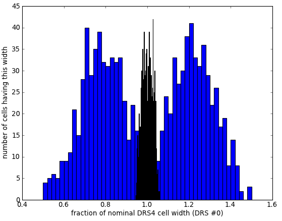
I managed to find a ping-pong distribution of cell widths that looks quite similar to that shown in Daniel's slides, using an algorithm similar to the technique one uses to find radial offsets in a tracking chamber (i.e. using residuals weighted by track slope), but I'd rather use the method with which you and Daniel have already found good results. (The attached graph shows in black the histogram of cell widths for essentially the algorithm used in DRS.cpp/DRSBoard::AnalyzeWF, and in blue the histogram of cell widths extracted from the slope-weighted residuals for a periodic reference signal.)
By the way, since Daniel finds a FWHM coincidence-timing resolution around 20-25ps at 5 GSPS (for perfectly identical pulses), should I expect a FWHM resolution (for synthesized, ideal pulses) of around 50-65ps at 2 GSPS?
(I'm posting here instead of writing you both privately because I figure there may be broader interest in Daniel's algorithm.)
-Bill
|
| Attachment 1: tcalib.png
|
|
|
768
|
Mon Aug 19 23:01:22 2019 |
Bill Ashmanskas | should one deassert DENABLE while writing the write-shift register? | Hi Stefan,
We have for some time now been using custom firmware on a custom board to read waveforms out of DRS4 chips. Now we are working on cascaded readout mode, 4 channels @ 2048 samples, WSREG=0x55, in order to allow for longer trigger latency.
Doing a testbench simulation of the FPGA code raised a question for me: Do I need to deassert DENABLE while I shift a new 8-bit value into the write-shift register? What happens if, during the few-hundred nanoseconds it takes to shift 8 bits into the register, the domino wave crosses cell 768, thereby shifting the write-shift register left by one bit? Is this shifting suppressed when A=0b1101? Or does the update of the actual write-shift register occur only once, after the 8th SRCLK cycle? (Maybe one is really shifting bits into a shadow register that is copied all at once into the actual register?)
I notice in simulating your drs4_eval5_app.vhd that if one sets bit 27 ("drs_ctl_dactive") of register 0 (do not deassert DENABLE on trigger), then starts the domino wave (set bit 0 of register 0), then issues a software trigger, then later writes to register 5 (config register, wsreg, etc.), DENABLE is not in fact deasserted during the time when A=0b1100 (conf_setup, conf_strobe) or when A=0b1101 (wsr_setup, wsr_strobe).
But my simulation testbench includes a simplified Verilog model of my interpretation of the DRS4 data sheet, and my simulated DRS4 happened to cause the write-shift register to shift (256 samples before DTAP toggled) during your "wsr_strobe" FSM state, thus corrupting the value that was being shifted into the WSREG via SRIN and SRCLK.
So I'm curious: to be safe, should one deassert DENABLE before updating the write-shift register, or is it safe to update it even while the domino wave is active and looping? It seems easy enough to be safe, since we should only need to write to the WSREG once during the setup phase and then let it loop forever.
Many thanks,
Bill
|
|