| ID |
Date |
Author |
Subject |
|
52
|
Thu Mar 11 11:45:52 2010 |
Stefan Ritt | Readout of DRS Data |
| Hao Huan wrote: |
|
Hi Stefan,
thanks to your help I can now successfully keep the Domino wave running at a stable frequency and maintain the channel cascading information in the Write Shift Register. (Since you told me WSR always reads and writes at the same time, I think I need to rewrite the information back every time after reading out from WSR to decide from which channel my data come, don't I?)
|
Yes you do. But if you have WSRLOOP=1 in the config register, this is done automatically. So the SR output is visible at the pin and will be fed back into the input.
| Hao Huan wrote: |
|
However I'm still having difficulty in reading out from the DRS cells. I use the ROI readout mode and assume as long as I give a pulse on RSRLOAD the data will come out one by one.
|
That's not correct. Have a look at Figure 14 of the datasheet. Do you see a single RSRLOAD pulse or many? There is only one RSRLOAD pulse to initialize the readout shift register, then the cells are clocked by SRCLK pulses.
| Hao Huan wrote: |
|
Also I read in the datasheet that WSROUT will give RSR output when DWRITE is low. Sometimes I see some random bits from this output and sometimes I see all zero's. What is the reasonable output I should see from WSROUT, say, when I'm running in the transparent mode with DWRITE low?
|
A single RSRLOAD pulse loads the RSR with a "1" at the domino stop position and "0" in all other places. A pulse on SRCLK shifts this "1" down the RSR. When it arrives at cell #1023, it will be visible for one clock cycle at WSROUT. The "double" functionality of WSROUT has the following background: Assume you use channel cascading 2x2048. Now the domino wave stopps in cell 1020 of the first channel for example. You have to read cells 1020,1021,1022,1024 of the first channel, then you continue with 0,1,2 on the second channel. But how do you know that you have to switch channels after the first four clock cycles? The SROUT output encodes the stop position (in this case 1020), but it needs 10 clock cycles before the information is available, so you don't have it after four cycles. That's where WSROUT comes into play: Since it outputs RSR bit by bit, it will show three "0", then a "1", when you are at cell 1023. Then you know that you have to switch channels immediately. That's why I output RSR via WSROUT if DWRITE is low.
|
|
54
|
Fri Mar 12 08:04:44 2010 |
Stefan Ritt | Input Bandwidth of the DRS Chip |
| Hao Huan wrote: |
|
I read in the DRS datasheet that the input bandwidth if 950MHz. However, it also says the output bandwidth in the transparent mode is 50MHz. Since in the transparent mode the input is routed to the output, does it mean the input bandwidth also gets reduced in the transparent mode? I don't know how the transparent mode works inside the chip of course, but this value would be important since if the hardware discriminators are connected to the output of DRS, we have to always work in the transparent mode.
|
In transparent mode, the input signal also gets routed to the output, where it goes through an output buffer, which limits the bandwidth to about 50 MHz, but only for the output. The effective bandwidth to the sampling cells is not changed. Please note however that the 950 MHz are for the "chip only". We measured this by keeping the input amplitude from a function generator constant at the input pin of the chip (measured with a high speed oscilloscope). Since each signal source has a non-zero impedance, the signal tends to "shrink" at high bandwidth, and we had to adjust the level of the function generator to keep the amplitude constant at high frequencies. If you do a realistic input stage with the THS4508 for example, the achievable bandwidth will be around 800 MHz. |
|
56
|
Thu Mar 18 22:10:41 2010 |
Stefan Ritt | Serial Interface Frequency of the DRS Chip |
| Hao Huan wrote: |
|
Thanks! The suggested algorithm looks promising. However, if the spikes take place only for those specific cells, is it possible to absorb them into the offset calibration?
|
No, since they are not constant. The bus segments charge up between readouts with a time constant of about 0.5s. So if you do the readout with 1Hz event rate and with 100Hz event rate, the peaks will differ by a factor up to 10, so a constant offset correction cannot take care of that. |
|
58
|
Mon Mar 22 09:12:19 2010 |
Stefan Ritt | PLL Loop Filter Configuration |
| Hao Huan wrote: |
|
in the datasheet it says at 6GSPS the typical loop filter parameters are 220Ω, 2.2nF and 27nF. If I want to run the Domino wave nominally at 1GHz, i.e. with a reference clock frequency around 0.5MHz, is there any recommended loop filter configuration? Is the setup of the evaluation board, that is, 220Ω, 3.3nF and 33nF an optimal choice?
|
The setup of the evaluation board is a good compromise which runs between 1 GHz and 5 GHz. Unfortunately I never found the time to investigate this in more detail. So if someone is willing to measure settling time and phase jitter with various combinations of R, C1 and C2, I'm more than happy to include this into the datasheet. |
|
64
|
Tue Apr 13 13:12:43 2010 |
Stefan Ritt | evaluation board used like a counter |
| lorenzo neri wrote: |
|
Hi all
it is possible to use the evaluation board like a counter?
I'm interested in the arriving time of all self trigger event in to a channel.
the input signal are 2V TTL of 10 ns at 50ohm, and the time acquisition window is 1 second.
|
The evaluation board is as good or bad as an digital oscilloscope to work like a counter. At 1 GSPS, you have a window of one microsecond, which is certainly too short for your application. |
|
65
|
Tue Apr 13 13:56:07 2010 |
Stefan Ritt | Baseline Variation In Data |
| Hao Huan wrote: |
|
Hi Stefan,
when I sample a constant input with the DRS 4 chip, there was a baseline variation showing up as a saw-tooth pattern which grows with the absolute value of the differential input. Do you think this is the kind of baseline variation mentioned in the evaluation board manual, i.e. coming from clock jitter in ADC sampling?
Thanks a lot!
|
Please post an oscilloscope screenshot here and I can tell you. |
|
66
|
Tue Apr 13 14:15:16 2010 |
Stefan Ritt | Simple example application to read a DRS evaluation board |
| Heejong Kim wrote: |
|
| Stefan Ritt wrote: |
|
Several people asked for s simple application to guide them in writing their own application to read out a DRS board. Such an application has been added in software revions 2.1.1 and is attached to this message. This example program drs_exam.cpp written in C++ does the following necessary steps to access a DRS board:
- Crate a "DRS" object and scan all USB devices
- Display found DRS boards
- Initialize the first found board and set the sampling frequency to 5 GSPS
- Enable internal trigger on channel #1 with 250 mV threshold
- Start acquisition and wait for a trigger
- Read two waveforms (both time and amplitude)
- Repeat this 10 times
I know that we are still missing a good documentation for the DRS API, but I have not yet found the time to do that. I hope the example program is enough for most people to start writing own programs. For Windows users (MS Visual C++ 8.0) there is a drs.sln project file, and for linux users there is a Makefile which can be used to compile this example program.
|
Hi, Stefan,
drs_exam.cpp is working good to read-out one board.
Now I would like to read-out two boards at the same time using the same trigger( external or internal).
I'm trying to understand and modify the original code for control two board.
Meantime, it would be very appreciated if you give any tips for this.
Thanks,
Heejong
|
The evaluation boards are not really made for multi-board applications. What you have to do is to maintain an external trigger which synchronizes the boards. So you need:
- two boards connected to two USB ports
- an external flip-flop connected to the two trigger inputs of both boards
If a trigger is sent to the flip-flop, it sends a trigger to both evaluation boards. You poll on one of the boards to see if it has triggered (vis IsBusy()), then you read out both boards. Now you have to reset the external flip-flop somehow from the computer. If you have a CAMAC I/O board or some other means of sending a logical signal to it, that could do the job. From the software point, you get a "DRS" object upon initialization, which contains then two "DRSBoard" objects, over which you can iterate. Look at the "drscl" program from the distribution on how to do that. |
|
67
|
Wed Apr 14 16:34:28 2010 |
Stefan Ritt | version 1.2 evaluation board with firmware 13279? |
| Heejong Kim wrote: |
Hi, Stefan,

I found that my collaborator bought 2 older version of evaluation board before.
They are the version 1.2 in plastics case with firmware 13191.

Can I upgrade the firmware from 13191 to 13279?
I'm wondering if the older version of evaluation board is working with firmware 13279.

Thanks,
Heejong
|
I checked and there is no significant difference between the two revisions, so I would just leave it. |
|
68
|
Thu Apr 15 13:48:40 2010 |
Stefan Ritt | ROFS Configuration |
| Hao Huan wrote: |
|
Hi Stefan,
according to the DRS4 datasheet, if we want an input range centered around U0, the ROFS should be 1.55V-U0. However when I read the codes of the evaluation board application, ROFS seems to be 1.6V-1.25*U0 where the coefficient 1.25 is said to come from sampling cell charge injection correction. Is it the right equation to use? What exactly does that charge injection correction mean?
Thanks a lot.
|
1.55V-U0 is the theoretical values, but there are certain "dirt" effects like chip-to-chip variation and charge injection. The difference between various chips is easily 20-30mV, so there is not a single "correct" value. The formula 1.6V-1.25*U0 I developed for a special evaluation board, where it kind of worked better than the theoretical value, but I never made systematic studies. One should average over several chips and use some solid average there. Best is if you try both formulas and check what give you the better linearity. |
|
70
|
Mon May 3 11:09:12 2010 |
Stefan Ritt | DRS4 chip model |
| Ignacio Diéguez Estremera wrote: |
|
Hi all,
i'm an electronics engineering student at UCM (Madrid) working on my master's thesis within the CTA collaboration. I'm designing the readout electronics for the telescope's camera, and i'm focusing in using GAPDs instead of PMTs and using the domino chip for the sampling of the signal. I was wondering if there is a spice and/or RF model of the DRS4 chip available. It would be very useful to perform some simulations before deciding to use the chip as the sampling solution for our prototypes.
If the answer is negative, can you give me some advise for modelling the chip in spice? Have you done any simulations?
Thanks in advance,
Ignacio Diéguez Estremera.
|
Yes there is a transistor-level spice model, which I used to design the chip, but you won't be happy with it: Given the 500,000+ transistors on the chip, a 100 ns simulation takes a couple of weeks. We tried to make a simplified model just for the analog input using some measured S-parameters, but found that the RF behavior of the chip is almost impossible to describe to better than let's say 50%. In the end you have to fine-tune your analog front-end experimentally, to obtain optimal bandwidth. We are just working on a reference design with gives you 850 MHz bandwidth using an active input buffer. |
|
72
|
Mon May 3 17:10:29 2010 |
Stefan Ritt | DRS4 chip model |
| Ignacio Diéguez Estremera wrote: |
|
| Stefan Ritt wrote: |
|
| Ignacio Diéguez Estremera wrote: |
|
Hi all,
i'm an electronics engineering student at UCM (Madrid) working on my master's thesis within the CTA collaboration. I'm designing the readout electronics for the telescope's camera, and i'm focusing in using GAPDs instead of PMTs and using the domino chip for the sampling of the signal. I was wondering if there is a spice and/or RF model of the DRS4 chip available. It would be very useful to perform some simulations before deciding to use the chip as the sampling solution for our prototypes.
If the answer is negative, can you give me some advise for modelling the chip in spice? Have you done any simulations?
Thanks in advance,
Ignacio Diéguez Estremera.
|
Yes there is a transistor-level spice model, which I used to design the chip, but you won't be happy with it: Given the 500,000+ transistors on the chip, a 100 ns simulation takes a couple of weeks. We tried to make a simplified model just for the analog input using some measured S-parameters, but found that the RF behavior of the chip is almost impossible to describe to better than let's say 50%. In the end you have to fine-tune your analog front-end experimentally, to obtain optimal bandwidth. We are just working on a reference design with gives you 850 MHz bandwidth using an active input buffer.
|
Thanks for the information.
I would like to try the huge :-) model. Can you send it to my email address? Since the input signal are pulses of a few nanoseconds at FHWM, the simulation time may be reduced. I will post some feedback in the forum once i give it a try.
Kind regards.
|
I just checked and realized that we are not allowed to give out the "huge" model since it contains parameters from the chip manufacturer's library which are confidentially. |
|
74
|
Tue May 4 11:26:21 2010 |
Stefan Ritt | DRS4 chip model |
| Ignacio Diéguez Estremera wrote: |
|
So i guess i won't be able to include drs4 in my simulations :-(. Any other suggestions? Maybe the S-params model you where working on? Anything is better than nothing :-)
|
Please find attached the S-parameters. |
|
77
|
Thu May 6 08:15:39 2010 |
Stefan Ritt | Random noise spec in datasheet |
| Ignacio Diéguez Estremera wrote: |
|
Hi,
According to DRS4's datasheet, the random noise is 0.35mVrms. Is this the input equivalent noise voltage? It is computed over the 0-950MHz frequency band?
Regards.
|
You cannot compare the DRS4 noise directly with an amplifier for example. The noise mainly comes from variations of the charge injection into the storage cells, and some noise during the readout process, which happens in a completely different frequency domain than the sampling.
So what I did is to keep the inputs open, measure a 1024-bin waveform, and compute the RMS of this waveform. So I believe that this is kind of equivalent noise voltage from 1-950 MHz. It does not start from zero since very low frequency noise (like 50 Hz) just causes a baseline shift and does not influence the RMS, but this is not so important since in most applications people do an event-by-event baseline subtraction to get rid of low frequency noise in their apparatus. The 0.35 mV RMS also depend on the electronics around the chip. On our USB evaluation board the noise it typically smaller (0.31 mV RMS), while in some VME board we measure 0.42 mV RMS. If you do the perfect analog design around the chip, you can maybe push this maybe even lower. |
|
79
|
Wed May 12 16:26:12 2010 |
Stefan Ritt | DRS4 chip model |
| Jinhong Wang wrote: |
|
| Stefan Ritt wrote: |
|
| Ignacio Diéguez Estremera wrote: |
|
So i guess i won't be able to include drs4 in my simulations :-(. Any other suggestions? Maybe the S-params model you where working on? Anything is better than nothing :-)
|
Please find attached the S-parameters.
|
Hi, we plan to do a time interpolating among the eight channels on a single chip to obtain a maximum 40 GSPS (or, maybe 30 GSPS ) sampling rate. Hence RF behavior of the anlog input is very important for us.
Will you give us some advice on the modeling of the anlog input circuit of the chip? Perhaps just the Spice model of the analog input?
The attached S parameters I found here is for fs =1 GSPS, what about fs=5GSPS?
thanks in advance,
Jinhong Wang (wangjinh@mail.ustc.edu.cn ; alleyor.wang@gmail.com)
|
To be honest, we never really succeeded to do any good simulation above let's say 500 MHz. We carefully tried to simulate the bond wire of the chip, the parasitic capacitances of the traces of the chip etc. but we always were off by a factor or two or so. Other groups reported the same problems. Some even did some 3D simulation model, without success. So our conclusion is that if you are interested in anything precise above 500 MHz, do a measurement.
So our current best design is with the THS4508. There is an AC coupled version going to 600 MHz, and a DC coupled version (uses more power) going to 800 MHz (-3dB). If you use passive inputs with a transformer for example, you can't go above 220 MHz. Next week I will publish both designs in this forum. |
|
81
|
Fri May 14 08:40:14 2010 |
Stefan Ritt | DVDD Problem of DRS 4 |
| Hao Huan wrote: |
|
Hi Stefan,
on our board some DRS chips draw a lot of current through DVDD after power-up and heat up significantly--it is true that our board doesn't have weak pull-down resistors at DENABLE and DWRITE output pins of FPGA, so this problem might have been caused by that, but a reinitialization of the Domino circuit doesn't help either. We tried different capacitors at DVDD and it seemed the larger the capacitance, the better the result--with a capacitor larger than 10nF some of the DRS chips could work happily in the normal way while if the capacitor is only 4.7nF all of them got very hot. Would you please provide some suggestions why there should be such a problem?
Thanks a lot!
|
I found that sometimes even a reinitialization fails if the pull-down resistors are missing. So instead playing with capacitors at DVDD, I would just solder two resistors on the board which should fix the problem completely. |
|
83
|
Tue May 18 08:23:07 2010 |
Stefan Ritt | DVDD Problem of DRS 4 |
| Hao Huan wrote: |
|
| Stefan Ritt wrote: |
|
| Hao Huan wrote: |
|
Hi Stefan,
on our board some DRS chips draw a lot of current through DVDD after power-up and heat up significantly--it is true that our board doesn't have weak pull-down resistors at DENABLE and DWRITE output pins of FPGA, so this problem might have been caused by that, but a reinitialization of the Domino circuit doesn't help either. We tried different capacitors at DVDD and it seemed the larger the capacitance, the better the result--with a capacitor larger than 10nF some of the DRS chips could work happily in the normal way while if the capacitor is only 4.7nF all of them got very hot. Would you please provide some suggestions why there should be such a problem?
Thanks a lot!
|
I found that sometimes even a reinitialization fails if the pull-down resistors are missing. So instead playing with capacitors at DVDD, I would just solder two resistors on the board which should fix the problem completely.
|
Thanks! After adding pull-down resistors the voltages come back to normal.
However there is another weird problem that arises: a reset pulse seems unable to set the internal shift registers to default values. For example, after reset without addressing the Config Register the PLL will not try to lock with external reference clock. Even if I explicitly address the Config Register after reset and have the PLL locked, some channels of the chip will give null output during readout while other channels work normally. Could it be that some channels are not initiated properly with the Domino circuit?
|
Something is wrong. I have 800 chips, and they all start up fine. Check with your scope the RESET, DSPEED, DENABLE and DTAP signals. When RESET is applied, DSPEED should go to 2.5 V. When DENABLE goes high, the domino wave is started and you should see DTAP toggle. DSPEED is then lowered by the PLL until DTAP matches your external reference clock. I usually keep DENABLE high all the time after initialization, so the domino wave just continues running.
Another problem could however be the chip readout. If some channel gives null output, it could be that your readout has a problem. Do you use RSRLOAD to initialize the readout sequence? |
|
84
|
Tue May 18 09:24:02 2010 |
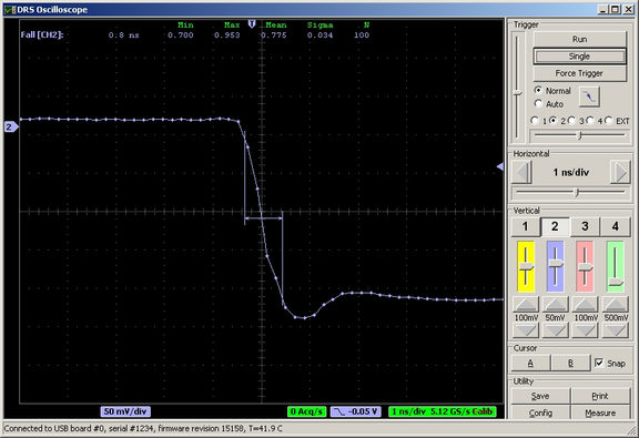
Stefan Ritt | Reference design for DRS4 active input buffer | The design of high frequency differential input stages with the DRS4 is a challenge, since the chip draws quite some current at the input (up to 1 mA at 5 GSPS), which must be sourced by the input buffer. A simple transformer as used in the DRS4 Evaluation Board 2.0 limits the bandwidth to 220 MHz. In meantime two active input stages have been worked out and successfully been tested, both utilizing the THS4508 differential amplifier. The first design is AC-coupled and uses less power, the second design is DC-coupled and uses more power with the benefit of delivering a higher bandwidth.
Both designs use a clamping diode at the input as a protection against high voltage spikes at the input. We used a RCLAMP0502B diode from SEMTECH, but any fast voltage suppressor diode will do the job.
The CMOFS input to the THS4508 set the common mode of the differential amplifier. In the AC version the level is set to mid-rail (2.5V), in the DC version it's set to 1.8V to match the input range of the DRS4.
The CAL+ and CAL- signals are used to bias the inputs to a well-defined DC level and can also be used to calibrate the chip. For bipolar inputs, they are both set to 0.8V. A positive 0.5V input pulse then drives DRS_IN+ to (0.8+0.25)V = 1.05V and DRS_IN- to (0.8-0.25)V = 0.55V. A negative 0.5V pulse then drives then DRS_IN+ to 0.55V and DRS_IN- to 1.05V. With ROFS=1.6V, the full dynamic range of the DRS4 is then used. Note that the THS4508 has a gain of 2, and the input has a -6dB voltage divider to compensate for that. To use other input ranges, such as -1V...0V, the CAL+ and CAL- signals can be adjusted accordingly. Note that the inputs of the DRS4 must always be between 0.1V and 1.5V.
AC-coupled version
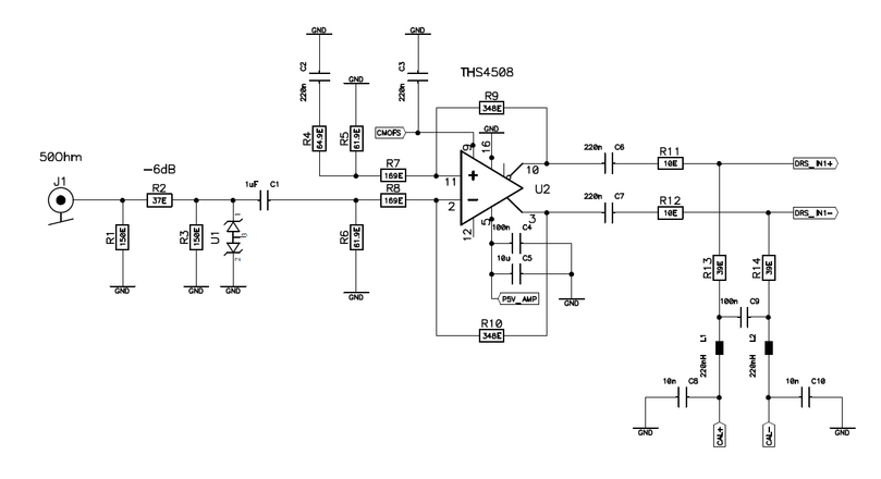
(click to enlarge)
Power supply: +5 V 40 mA
Bandwidth (-3dB): 600 MHz
CMOFS: 2.5 V
Transfer function:
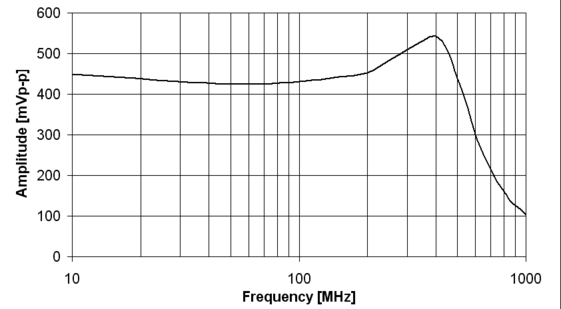
(click to enlarge)
The transfer function was measured by applying a fixed amplitude sine wave to the input, and measuring the peak-to-peak value of the read out waveform with the DRSOsc application.
DC-coupled Version
The DC-coupled version has a slightly higher power consumption since there is a constant current flowing through the output into the DRS4 chip. On the other hand, the bandwidth is a bit higher and the peaking around 400 MHz is a bit smaller. The input is still AC-coupled, so both positive and negative pulses can be accepted.
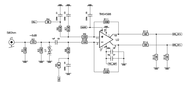
(click to enlarge)
Power supply: +5 V 115 mA
Bandwidth (-3dB): 800 MHz
CMOFS: 1.8 V
Transfer function:
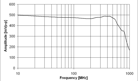
(click to enlarge)
Achievable performance
With the active input stage, much faster rise- and fall times can be achieved. Following picture shows a signal from a external clock having a fall time of about 300 ps being recorded with the AC-coupled version of the active input stage. The fall time of the recorded signal is about 800 ps, which is about the minimum which can be achieved with the AC-coupled version. The DC-coupled version achieves about 700ps.
|
|
86
|
Wed May 19 09:16:02 2010 |
Stefan Ritt | DVDD Problem of DRS 4 |
| Hao Huan wrote: |
|
| Stefan Ritt wrote: |
|
| Hao Huan wrote: |
|
| Stefan Ritt wrote: |
|
| Hao Huan wrote: |
|
Hi Stefan,
on our board some DRS chips draw a lot of current through DVDD after power-up and heat up significantly--it is true that our board doesn't have weak pull-down resistors at DENABLE and DWRITE output pins of FPGA, so this problem might have been caused by that, but a reinitialization of the Domino circuit doesn't help either. We tried different capacitors at DVDD and it seemed the larger the capacitance, the better the result--with a capacitor larger than 10nF some of the DRS chips could work happily in the normal way while if the capacitor is only 4.7nF all of them got very hot. Would you please provide some suggestions why there should be such a problem?
Thanks a lot!
|
I found that sometimes even a reinitialization fails if the pull-down resistors are missing. So instead playing with capacitors at DVDD, I would just solder two resistors on the board which should fix the problem completely.
|
Thanks! After adding pull-down resistors the voltages come back to normal.
However there is another weird problem that arises: a reset pulse seems unable to set the internal shift registers to default values. For example, after reset without addressing the Config Register the PLL will not try to lock with external reference clock. Even if I explicitly address the Config Register after reset and have the PLL locked, some channels of the chip will give null output during readout while other channels work normally. Could it be that some channels are not initiated properly with the Domino circuit?
|
Something is wrong. I have 800 chips, and they all start up fine. Check with your scope the RESET, DSPEED, DENABLE and DTAP signals. When RESET is applied, DSPEED should go to 2.5 V. When DENABLE goes high, the domino wave is started and you should see DTAP toggle. DSPEED is then lowered by the PLL until DTAP matches your external reference clock. I usually keep DENABLE high all the time after initialization, so the domino wave just continues running.
Another problem could however be the chip readout. If some channel gives null output, it could be that your readout has a problem. Do you use RSRLOAD to initialize the readout sequence?
|
Yes; I used RSRLOAD to trigger readout of all channels in parallel so the asymmetry between channels of the same chip is really a big puzzle. Also during reset DSPEED indeed goes to 2.5V, but after reset the PLL will not try to lock with the external reference clock and lower DSPEED. Instead the Domino circuit just oscillates at the highest frequency by itself.
A more confusing discovery is that the SRIN level before starting the Domino wave could affect the behavior of the PLL. I mean the level of SRIN when the chip is at A="1111" or "1010". Is SRIN supposed to influence the chip even in these standby or transparent modes?
|
Just some ideas:
- Is DENABLE really kept high all the time?
- Is DRESET only applied once during initialization, after that it should stay high
- Does REFCLK+/REFCLK- really toggle at the required sampling speed / 2048?
- Is the REFCLK really a good differential signal? Note that it must be biased properly since the DRS4 inputs are high impedance
- Is the Bit1 in the Config Register really at "1" to enable the PLL?
The only way the SRIN level could affect the PLL is if you address the Config Register (A="1100") and you clock in a few bits with SRCLK.
Have you thought about 'crazy' things such as:
- Defining the DRS4 chip wronly in your CAD software so that the pins are different from what you think?
- Some soldering problem of the DRS4 chips (we had this in the past) so that some pins are not connected at all and others have shorts
I guess you checked most of the things, so I'm just wildly guessing in order to stimulate some thoughts.
The ultimate check would be to get one of the evaluation boards (I sent a few to Jean-Francois Genat some time ago...) and compare the DRS4 signals pin by pin. |
|
88
|
Tue Jun 1 13:36:18 2010 |
Stefan Ritt | High Frequency Input for DRS |
| Hao Huan wrote: |
|
Hi Stefan,
I read in the DRS datasheet that the bandwidth for the transparent mode OUT+ is only 200MHz which I think cannot be improved by any active input buffer; so if you want to operate the chip for really high frequency input, would it be better to feed on-board discriminators not from the output of DRS but from the input end?
Thanks!
|
First, the 200 MHz is not correct. Table 1 clearly states ANALOG OUTPUTS - Bandwidth (-3dB): 50 MHz. This is also shown in plot 11 (revision 0.9). But that does not necessarily mean that you have to drive your discriminators from the input of the DRS4 chip. If you use this for triggering, a 1-2 ns timing jitter does not matter, since stopping the domino wave anyhow has a 3-4 cell jitter. If you send a very fast signal though a 50 MHz low pass filter, the timing anyhow doe not change, only the slope of your signal gets lower, so you are more sensitive to noise, which in turn causes the 1-2 ns timing jitter. But I personally would not worry about that too much. Putting any signal splitting components in the input path would reduce the input bandwidth, which would be much more of an issue. |
|
92
|
Fri Jun 18 11:45:18 2010 |
Stefan Ritt | DVDD Problem of DRS 4 |
| Jinhong Wang wrote: |
|
Hi Stefan
I designed the evaluation board for our experiment. On our boards, I encountered the similar problem when working on the PLL of DRS4. I compared the following two configuration process, which on with PLL locked, the other not,
Process1:
step 1: Set DEnable and DWrite low,
Step2 : Reset DRS4 with a negative pulse of about 900 ns
Step3: Set DEnable high, thus do nothing but wait
I found DRS4 PLL working and locked.
Process 2:
Step 1: Set DEnable and DWrite low,
Step2 : Reset DRS4 with a negative pulse of about 900 ns
Step3: Set Config. Register( "11111111" .of course, this step was not necessary, just to see whether SPI was working properly from DTAP when set to "11111110")
Step4: Set The read shift Register ( full read out mode)
Step5: Set DEnable high,
Step6: Set DWrite high , thus low it , and prepare to read the waveform.
Well, I found in this case, the PLL was not locked, I am sure there was no problem with my SPI configuration process of DRS4.
toggle from DTAP could be viewed, but not stable.
Any Suggestions ?
thanks.
|
So the main difference, if I understand correctly, is the setting of the Config Register. Actually I never tried that, I always went with the default settings (all "1"). What happens if you write "00000000"? You know Bit1 controls the PLL, maybe there is a bug and the signal needs to be inverted. |
|