| ID |
Date |
Author |
Subject |
|
725
|
Thu Nov 8 11:54:33 2018 |
Stefan Ritt | Timing Issue | That's not a bug, but a feature of the DRS4 chip. The time bins have different values by the properties of the chip. They are generated by a chain of inverters, which all have different propagation times. This delay is measured by the time calibration and then applied. If you want equidistant bins,
you have to interpolate your data points (linearly or by splines) and resample the signal. You can find more details in the DRS4 data sheet.
Best,
Stefan
> Hi,
>
> We are using the DRS4 Evaluation Board as a digitizer in our laboratory.
> We found a strange behavior in the saved files, more specifically the time difference between two consecutive points is not constant, also after the Timing Calibration.
> As an example, I paste a piece of a xml file saved using the drsosc program, acquiring CH1 (open):
>
> ---------------------------
> ---[ START XML EXAMPLE ]---
> ---------------------------
>
> <?xml version="1.0" encoding="ISO-8859-1"?>
> <!-- created by MXML on Thu Nov 8 11:13:27 2018 -->
> <DRSOSC>
> <Event>
> <Serial>1</Serial>
> <Time>2018/11/08 11:13:27.163</Time>
> <HUnit>ns</HUnit>
> <VUnit>mV</VUnit>
> <Board_2796>
> <Trigger_Cell>216</Trigger_Cell>
> <Scaler0>0</Scaler0>
> <CHN1>
> <Data>0.000,-1.0</Data>
> <Data>1.083,-1.0</Data>
> <Data>2.143,-1.0</Data>
> <Data>2.926,-1.0</Data>
> <Data>4.249,-0.1</Data>
> <Data>4.929,-0.6</Data>
> <Data>6.075,-0.4</Data>
> <Data>7.042,0.0</Data>
> <Data>8.299,0.2</Data>
>
> [...]
>
> -------------------------
> ---[ END XML EXAMPLE ]---
> -------------------------
>
> We found the same behavior saving events in the binary format, and then reading them with the read_binary.cpp
>
> Is there a way to fix our issue?
>
> Thanks a lot
>
> Davide and Alessio |
|
724
|
Thu Nov 8 11:44:35 2018 |
Davide Depaoli | Timing Issue | Hi,
We are using the DRS4 Evaluation Board as a digitizer in our laboratory.
We found a strange behavior in the saved files, more specifically the time difference between two consecutive points is not constant, also after the Timing Calibration.
As an example, I paste a piece of a xml file saved using the drsosc program, acquiring CH1 (open):
---------------------------
---[ START XML EXAMPLE ]---
---------------------------
<?xml version="1.0" encoding="ISO-8859-1"?>
<!-- created by MXML on Thu Nov 8 11:13:27 2018 -->
<DRSOSC>
<Event>
<Serial>1</Serial>
<Time>2018/11/08 11:13:27.163</Time>
<HUnit>ns</HUnit>
<VUnit>mV</VUnit>
<Board_2796>
<Trigger_Cell>216</Trigger_Cell>
<Scaler0>0</Scaler0>
<CHN1>
<Data>0.000,-1.0</Data>
<Data>1.083,-1.0</Data>
<Data>2.143,-1.0</Data>
<Data>2.926,-1.0</Data>
<Data>4.249,-0.1</Data>
<Data>4.929,-0.6</Data>
<Data>6.075,-0.4</Data>
<Data>7.042,0.0</Data>
<Data>8.299,0.2</Data>
[...]
-------------------------
---[ END XML EXAMPLE ]---
-------------------------
We found the same behavior saving events in the binary format, and then reading them with the read_binary.cpp
Is there a way to fix our issue?
Thanks a lot
Davide and Alessio |
|
723
|
Thu Nov 8 09:57:26 2018 |
Stefan Ritt | Pi attenuator on eval board inputs? | The attenuator compensates for the gain of the buffer which is slightly above one. In addition, it serves as a "placeholder" in case one wants larger input signals. One can easily convert the attenuator to -6db, -12db, etc. by chaning the resistors.
Stefan
| Sean Quinn wrote: |
|
Dear DRS4 team,
I am curious about this part of the circuit:
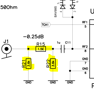
What is the purpose of this?
|
|
|
722
|
Mon Nov 5 17:17:08 2018 |
Sean Quinn | Pi attenuator on eval board inputs? | Dear DRS4 team,
I am curious about this part of the circuit:
What is the purpose of this? |
|
721
|
Wed Sep 26 19:21:03 2018 |
Stefan Ritt | Trigger OUT pulse width variable from 100 us up to 100 ms | In meantime I even updated the manual.
Stefan
| Gerard Arino-Estrada wrote: |
|
Thank you very much for the answer, I really appreciate your help.
Thanks!
Gerard
|
|
|
720
|
Wed Sep 26 18:28:20 2018 |
Gerard Arino-Estrada | Trigger OUT pulse width variable from 100 us up to 100 ms | Thank you very much for the answer, I really appreciate your help.
Thanks!
Gerard
| Stefan Ritt wrote: |
|
The "Trigger OUT" has changed recently. It goes high on a new trigger, but then STAYS high until the board has been read out by the PC and re-started. This allows better synchronization with some external trigger, which can be re-armed with the falling edge of the trigger out signal. The signal can be quite long, since readout of an event via USB typically takes 2 ms, but can be more if the PC is busy. If you need back your 150 ns pulse, send the trigger out to an external pulse shaper with fixed shaping width.
Stefan
| Gerard Arino-Estrada wrote: |
|
Hello Stefan,
I am using the DRS4 board connected to a Raspberry PI and through the drsosc application. I am interested on using the "Trigger OUT" signal to do some extra data processing with NIM modules. According to the manual, for each hardware trigger a TTL pulse of 150 ns width should be send through the "trigger OUT". In my case I do see pulses with widths ranging from 100 microseconds up to hundreds of miliseconds. I am connecting the signal directly to an oscilloscope with 50 Ohm termination. I have tried two DRS4 boards in identical conditions and both show the same behavior. Having such wide and variable pulses makes it complicated for me to do the extra post-processing. Have you any idea of what might be going wrong? Thank you very much.
Best regards,
Gerard
|
|
|
|
Draft
|
Wed Sep 26 18:25:07 2018 |
Gerard Arino-Estrada | Trigger OUT pulse width variable from 100 us up to 100 ms | Thank you very much for the answer, I really appreciate your help.
Thanks!
Gerard
| Stefan Ritt wrote: |
|
The "Trigger OUT" has changed recently. It goes high on a new trigger, but then STAYS high until the board has been read out by the PC and re-started. This allows better synchronization with some external trigger, which can be re-armed with the falling edge of the trigger out signal. The signal can be quite long, since readout of an event via USB typically takes 2 ms, but can be more if the PC is busy. If you need back your 150 ns pulse, send the trigger out to an external pulse shaper with fixed shaping width.
Stefan
| Gerard Arino-Estrada wrote: |
|
Hello Stefan,
I am using the DRS4 board connected to a Raspberry PI and through the drsosc application. I am interested on using the "Trigger OUT" signal to do some extra data processing with NIM modules. According to the manual, for each hardware trigger a TTL pulse of 150 ns width should be send through the "trigger OUT". In my case I do see pulses with widths ranging from 100 microseconds up to hundreds of miliseconds. I am connecting the signal directly to an oscilloscope with 50 Ohm termination. I have tried two DRS4 boards in identical conditions and both show the same behavior. Having such wide and variable pulses makes it complicated for me to do the extra post-processing. Have you any idea of what might be going wrong? Thank you very much.
Best regards,
Gerard
|
|
|
|
718
|
Wed Sep 26 14:44:14 2018 |
Stefan Ritt | Trigger OUT pulse width variable from 100 us up to 100 ms | The "Trigger OUT" has changed recently. It goes high on a new trigger, but then STAYS high until the board has been read out by the PC and re-started. This allows better synchronization with some external trigger, which can be re-armed with the falling edge of the trigger out signal. The signal can be quite long, since readout of an event via USB typically takes 2 ms, but can be more if the PC is busy. If you need back your 150 ns pulse, send the trigger out to an external pulse shaper with fixed shaping width.
Stefan
| Gerard Arino-Estrada wrote: |
|
Hello Stefan,
I am using the DRS4 board connected to a Raspberry PI and through the drsosc application. I am interested on using the "Trigger OUT" signal to do some extra data processing with NIM modules. According to the manual, for each hardware trigger a TTL pulse of 150 ns width should be send through the "trigger OUT". In my case I do see pulses with widths ranging from 100 microseconds up to hundreds of miliseconds. I am connecting the signal directly to an oscilloscope with 50 Ohm termination. I have tried two DRS4 boards in identical conditions and both show the same behavior. Having such wide and variable pulses makes it complicated for me to do the extra post-processing. Have you any idea of what might be going wrong? Thank you very much.
Best regards,
Gerard
|
|
|
717
|
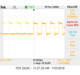
Sun Sep 23 02:22:46 2018 |
Gerard Arino-Estrada | Trigger OUT pulse width variable from 100 us up to 100 ms | Hello Stefan,
I am using the DRS4 board connected to a Raspberry PI and through the drsosc application. I am interested on using the "Trigger OUT" signal to do some extra data processing with NIM modules. According to the manual, for each hardware trigger a TTL pulse of 150 ns width should be send through the "trigger OUT". In my case I do see pulses with widths ranging from 100 microseconds up to hundreds of miliseconds. I am connecting the signal directly to an oscilloscope with 50 Ohm termination. I have tried two DRS4 boards in identical conditions and both show the same behavior. Having such wide and variable pulses makes it complicated for me to do the extra post-processing. Have you any idea of what might be going wrong? Thank you very much.
Best regards,
Gerard |
|
716
|
Thu Sep 13 18:09:13 2018 |
Martin Petriska | "Symmetric spikes" fixed | Ok, so I made it ... and Yes it works :),
https://youtu.be/0noy4CoFoh8
here is changed part in drs4_eval4_app.vhd
        when done =>

          drs_readout_state    <= spikeoff;

          drs_stat_busy        <= '0';

          drs_dpram_we1        <= '0';

          drs_write_set        <= '1';   -- set drs_write_ff in proc_drs_write

                                         -- to keep chip "warm"
 -- spike fix ELOG 697


          when spikeoff =>

            o_drs_addr       <= "1011"; -- Address the read shift register by applying 1011b to A3:A0

            o_drs_srin       <= '0'; -- Switch SRIN low

             drs_readout_state                 <= spikecycle;

             -- Apply 1024 clock cycles to SRCLK

             drs_sr_count         <= 0;
          when spikecycle =>

             drs_sr_count         <= drs_sr_count + 1;

             o_drs_srclk          <= not o_drs_srclk;

             if (drs_sr_count = 1024) then

                drs_readout_state <= idle;

             end if;
-- set-up of configuration register
| Stefan Ritt wrote: |
|
Yes it's possible, but I have to find time for that. The software of the evaluation board takes care of the spikes ("remove spikes"), so I thought it's not so urgent to fix that in the FPGA (which takes me some time).
Stefan
| Martin Petriska wrote: |
|
Hi,
Is it possible to fix it by FPGA changes? I see readout cycle (proc_drs_reedout) in drs4_eval(4)5_app.vhd, but not sure where to exactly put this three commands. Could you please attach app.vhd file for eval board with example how to fix ?
Regards,
Martin
| Stefan Ritt wrote: |
|
Good news for all DRS4 users. After many years, I finally understand where the "symmetric spikes" come from and how to fix them.
The "symmetric spikes" are small spikes of 17-18mV, which randomly happen at 1-2 cells. They alwas come in groups of 2 in each channel, symmetric around sampling cell #512. See first attachment.
The reason for the spikes is the previous readout cycle. On each readout cycle, the "read bit" is clocked through all 1024 cells to switch one cell contents to the DRS4 output. At the end of the 1024 cycles, the read bit stays at its last position. The bit is carried by a metal line on the chip, which crosses all 9 channels (second attachment). This bit now influences the sampling cells below the metal line capacitively, so their contents is "pushed up" by a few mV, just like the ROFS offset does. Since the DRS sampling channels are in a snake layout, going 0-512 from left, then 512-1023 back again, the line crosses two cells in each channel, and thus the symmetric spikes.
Previously, there was a software solution for that. In the evaluation board software DRSOsc there is a button "Remove spikes" which tries to fix this in software. Although this works most of the time, it's annoying and not 100% safe. Like when the spike sits on top of a noise signal, it might not be recognized. Fixing this in hardware is however straight forwar. After the readout cycle ends, push the read bit out of the chip:
- Address the read shift register by applying 1011b to A3:A0
- Switch SRIN low
- Apply 1024 clock cycles to SRCLK
This shifts the bit out of the chip, so that the next event is not affected by the read bit. The third attachment show the effect of this. The "clear cycle" increases the readout time a little bit, but depending on the application this might be worth it.
Regards,
Stefan
|
|
|
|
|
715
|
Tue Sep 4 13:04:30 2018 |
Stefan Ritt | "Symmetric spikes" fixed | Yes it's possible, but I have to find time for that. The software of the evaluation board takes care of the spikes ("remove spikes"), so I thought it's not so urgent to fix that in the FPGA (which takes me some time).
Stefan
| Martin Petriska wrote: |
|
Hi,
Is it possible to fix it by FPGA changes? I see readout cycle (proc_drs_reedout) in drs4_eval(4)5_app.vhd, but not sure where to exactly put this three commands. Could you please attach app.vhd file for eval board with example how to fix ?
Regards,
Martin
| Stefan Ritt wrote: |
|
Good news for all DRS4 users. After many years, I finally understand where the "symmetric spikes" come from and how to fix them.
The "symmetric spikes" are small spikes of 17-18mV, which randomly happen at 1-2 cells. They alwas come in groups of 2 in each channel, symmetric around sampling cell #512. See first attachment.
The reason for the spikes is the previous readout cycle. On each readout cycle, the "read bit" is clocked through all 1024 cells to switch one cell contents to the DRS4 output. At the end of the 1024 cycles, the read bit stays at its last position. The bit is carried by a metal line on the chip, which crosses all 9 channels (second attachment). This bit now influences the sampling cells below the metal line capacitively, so their contents is "pushed up" by a few mV, just like the ROFS offset does. Since the DRS sampling channels are in a snake layout, going 0-512 from left, then 512-1023 back again, the line crosses two cells in each channel, and thus the symmetric spikes.
Previously, there was a software solution for that. In the evaluation board software DRSOsc there is a button "Remove spikes" which tries to fix this in software. Although this works most of the time, it's annoying and not 100% safe. Like when the spike sits on top of a noise signal, it might not be recognized. Fixing this in hardware is however straight forwar. After the readout cycle ends, push the read bit out of the chip:
- Address the read shift register by applying 1011b to A3:A0
- Switch SRIN low
- Apply 1024 clock cycles to SRCLK
This shifts the bit out of the chip, so that the next event is not affected by the read bit. The third attachment show the effect of this. The "clear cycle" increases the readout time a little bit, but depending on the application this might be worth it.
Regards,
Stefan
|
|
|
|
714
|
Mon Sep 3 11:17:26 2018 |
Martin Petriska | "Symmetric spikes" fixed | Hi,
Is it possible to fix it by FPGA changes? I see readout cycle (proc_drs_reedout) in drs4_eval(4)5_app.vhd, but not sure where to exactly put this three commands. Could you please attach app.vhd file for eval board with example how to fix ?
Regards,
Martin
| Stefan Ritt wrote: |
|
Good news for all DRS4 users. After many years, I finally understand where the "symmetric spikes" come from and how to fix them.
The "symmetric spikes" are small spikes of 17-18mV, which randomly happen at 1-2 cells. They alwas come in groups of 2 in each channel, symmetric around sampling cell #512. See first attachment.
The reason for the spikes is the previous readout cycle. On each readout cycle, the "read bit" is clocked through all 1024 cells to switch one cell contents to the DRS4 output. At the end of the 1024 cycles, the read bit stays at its last position. The bit is carried by a metal line on the chip, which crosses all 9 channels (second attachment). This bit now influences the sampling cells below the metal line capacitively, so their contents is "pushed up" by a few mV, just like the ROFS offset does. Since the DRS sampling channels are in a snake layout, going 0-512 from left, then 512-1023 back again, the line crosses two cells in each channel, and thus the symmetric spikes.
Previously, there was a software solution for that. In the evaluation board software DRSOsc there is a button "Remove spikes" which tries to fix this in software. Although this works most of the time, it's annoying and not 100% safe. Like when the spike sits on top of a noise signal, it might not be recognized. Fixing this in hardware is however straight forwar. After the readout cycle ends, push the read bit out of the chip:
- Address the read shift register by applying 1011b to A3:A0
- Switch SRIN low
- Apply 1024 clock cycles to SRCLK
This shifts the bit out of the chip, so that the next event is not affected by the read bit. The third attachment show the effect of this. The "clear cycle" increases the readout time a little bit, but depending on the application this might be worth it.
Regards,
Stefan
|
|
|
713
|
Tue Aug 21 14:36:44 2018 |
Stefan Ritt | Optimal readout speed | The analog output of the DRS4 chip needs some time to settle. In principle it need an infinite amout of time (exponential curve) to settle to 100% of the final value. So if we sample after a finite time, there is some error we do. Some of the error will be taken care of the voltage calibration, but there remains some residual error depending on the value of the previous sampling cell. So all sampling speeds 10 MHz, 16 MHz, 33 MHz are kind of rule of thumbs. In the end we run the evaluation board at 16 MHz to save a little bit of power (which is limited on an USB device). But I never made a careful study of noise-after-calibration vs. sampling speed. If you have some measurements, I'm happt to include it in the data sheet.
Stefan
| Sean Quinn wrote: |
|
Dear DRS4 team,
On page 3 of the data sheet, Table 1. for readout speed a typical value of 10 MHz is specified, but in the comment column it notes optimal performance achieved at 33 MHz.
I see the V5.1 eval board runs at 16 MHz. I'd like to understand the rationale for this using speed, instead of 33 MHz. Is there an SNR issue for the ADC at the higher speed, even though this is optimal for the DRS4?
Very best,
Sean
|
|
|
712
|
Tue Aug 14 06:10:49 2018 |
Stefan Ritt | Latch delay support | I put that on the wish list, but I won't have time for that in the next months.
Stefan
| Martin Petriska wrote: |
|
Hi,
https://forge.physik.rwth-aachen.de/projects/drs4-rwth
Not sure about their licensing, but is it possible to add latch delay support to official firmware ?
Best regards
Martin
|
|
|
711
|
Mon Aug 13 19:44:59 2018 |
Martin Petriska | Latch delay support | Hi,
https://forge.physik.rwth-aachen.de/projects/drs4-rwth
Not sure about their licensing, but is it possible to add latch delay support to official firmware ?
Best regards
Martin |
|
710
|
Wed Aug 1 00:49:30 2018 |
Sean Quinn | Optimal readout speed | Dear DRS4 team,
On page 3 of the data sheet, Table 1. for readout speed a typical value of 10 MHz is specified, but in the comment column it notes optimal performance achieved at 33 MHz.
I see the V5.1 eval board runs at 16 MHz. I'd like to understand the rationale for this using speed, instead of 33 MHz. Is there an SNR issue for the ADC at the higher speed, even though this is optimal for the DRS4?
Very best,
Sean |
|
709
|
Fri Jul 20 00:44:13 2018 |
Woon-Seng Choong | Effect of interpolation on timing | Just a follow-up update.
It turns out that I was using a cubic spline interpolation with smoothing. If I required the cubic spline to go through the sampled points, then I obtained similar time resolution as the simple linear interpolation.
| Woon-Seng Choong wrote: |
|
Using a test pulse split into two channels of the DRS4 Evaluation Board v5, I looked at the time resolution using a leading edge threshold. The voltage and timing calibration was performed. One method (1) is to linearly interpolate between two points of the raw waveform that is above and below the threshold (this is exactly the algorithm given in read_binary.c in the drs4 source distribution); and another (2) is to use a cubic spline interpolation of the raw waveform. The results I obtained are:
Method 1: dt = 1.298 ns +/- 7.22 ps
Method 2: dt = 1.293 ns +/- 15.48 ps
I am really puzzled why the time resolution of the spline interpolation is about a factor 2 worse than the simple linear interpolation. Has anyone studied the time resolution using similar or other interpolation methods?
|
|
|
708
|
Mon Jul 16 19:39:35 2018 |
Woon-Seng Choong | Effect of interpolation on timing | Using a test pulse split into two channels of the DRS4 Evaluation Board v5, I looked at the time resolution using a leading edge threshold. The voltage and timing calibration was performed. One method (1) is to linearly interpolate between two points of the raw waveform that is above and below the threshold (this is exactly the algorithm given in read_binary.c in the drs4 source distribution); and another (2) is to use a cubic spline interpolation of the raw waveform. The results I obtained are:
Method 1: dt = 1.298 ns +/- 7.22 ps
Method 2: dt = 1.293 ns +/- 15.48 ps
I am really puzzled why the time resolution of the spline interpolation is about a factor 2 worse than the simple linear interpolation. Has anyone studied the time resolution using similar or other interpolation methods?
|
|
707
|
Fri Jun 29 07:51:33 2018 |
Stefan Ritt | Negative Bin Width | Yes that's normal. A negative cell bin width means that the next cell N+1 samples the input signal before cell N. This can happen due to the signal routing on the DRS4 chip.
Stefan
| Woon-Seng Choong wrote: |
|
I am using a DRS4 Evaluation Board v5 and running the drsosc.exe version 5.06 on a Window 7 machine. I have performed the voltage and timing calibration.
With test pulses on channel 1 and 2, I collected binary data file with all 4 channels active sampling at 5GSPS.
Attached is a distribution of the bin_width vs. cell # for all the 4 channels. Note that there are few cells with bin_width < 10 ps.
Channel 1: bin_width[498] = -0.000348, bin_width[1010]= -0.000348
Channel 2: bin_width[498] = 0.007363
Channel 3: bin_width[498] = 0.007843
Channel 4: bin_width[498] = 0.005948
Is this normal? How can you get negative bin_width? What does negative bin_width means?
I have attached the binary data file for your verification.
|
|
|
706
|
Thu Jun 28 19:55:45 2018 |
Woon-Seng Choong | Negative Bin Width | I am using a DRS4 Evaluation Board v5 and running the drsosc.exe version 5.06 on a Window 7 machine. I have performed the voltage and timing calibration.
With test pulses on channel 1 and 2, I collected binary data file with all 4 channels active sampling at 5GSPS.
Attached is a distribution of the bin_width vs. cell # for all the 4 channels. Note that there are few cells with bin_width < 10 ps.
Channel 1: bin_width[498] = -0.000348, bin_width[1010]= -0.000348
Channel 2: bin_width[498] = 0.007363
Channel 3: bin_width[498] = 0.007843
Channel 4: bin_width[498] = 0.005948
Is this normal? How can you get negative bin_width? What does negative bin_width means?
I have attached the binary data file for your verification.
|
|