| ID |
Date |
Author |
Subject |
|
62
|
Fri Apr 9 17:14:45 2010 |
Hao Huan | Baseline Variation In Data |
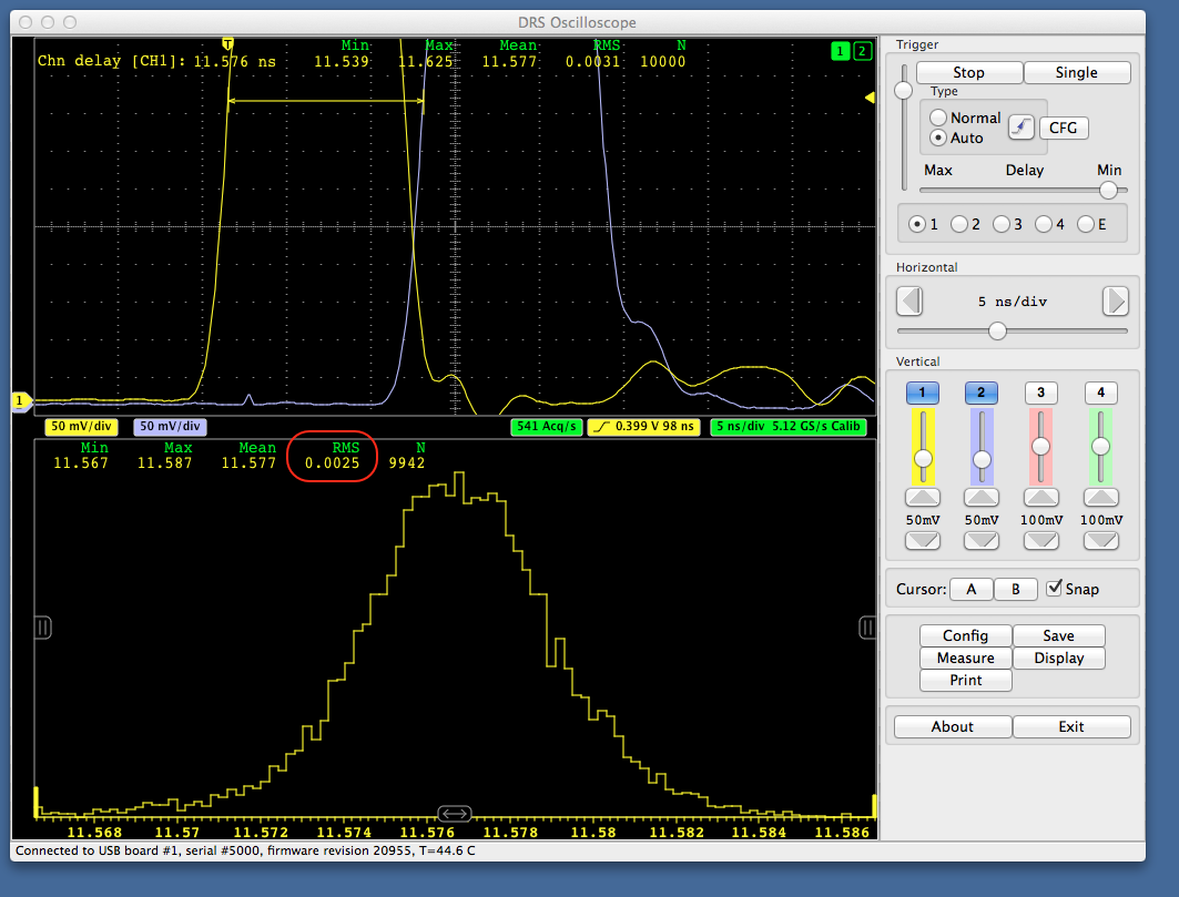
Hi Stefan,
when I sample a constant input with the DRS 4 chip, there was a baseline variation showing up as a saw-tooth pattern which grows with the absolute value of the differential input. Do you think this is the kind of baseline variation mentioned in the evaluation board manual, i.e. coming from clock jitter in ADC sampling?
Thanks a lot!
|
|
65
|
Tue Apr 13 13:56:07 2010 |
Stefan Ritt | Baseline Variation In Data |
| Hao Huan wrote: |
|
Hi Stefan,
when I sample a constant input with the DRS 4 chip, there was a baseline variation showing up as a saw-tooth pattern which grows with the absolute value of the differential input. Do you think this is the kind of baseline variation mentioned in the evaluation board manual, i.e. coming from clock jitter in ADC sampling?
Thanks a lot!
|
Please post an oscilloscope screenshot here and I can tell you. |
|
17
|
Mon Oct 19 09:06:43 2009 |
Jinhong Wang | BIAS Pin of DRS4 |
Dear Mr. Stefan Ritt.
Thank u for your timely response on "DSR4 Full Readout Mode", I received it from Professor Qi An, who is my PhD supervisor.
I am currently going through the DRS4 datasheet. Well, can you give some specification on the usage of "BIAS" pin of DRS4? It is just metioned in the datasheet as bias of internal buffer. What is the internal buffer exactly reffered to here? The MUXOUT buffer of channel 8 or else? Does it have some relationship to O_OFS? I mean, if the reference voltage to BIAS is changed, how will the output be influenced?
Looking forward to hearing from you soon.
Jinhong Wang
Fast Electronics LAB. of University of Science and Technology of China. |
|
18
|
Mon Oct 19 09:13:00 2009 |
Stefan Ritt | BIAS Pin of DRS4 |
| Jinhong Wang wrote: |
|
Dear Mr. Stefan Ritt.
Thank u for your timely response on "DSR4 Full Readout Mode", I received it from Professor Qi An, who is my PhD supervisor.
I am currently going through the DRS4 datasheet. Well, can you give some specification on the usage of "BIAS" pin of DRS4? It is just metioned in the datasheet as bias of internal buffer. What is the internal buffer exactly reffered to here? The MUXOUT buffer of channel 8 or else? Does it have some relationship to O_OFS? I mean, if the reference voltage to BIAS is changed, how will the output be influenced?
Looking forward to hearing from you soon.
Jinhong Wang
Fast Electronics LAB. of University of Science and Technology of China.
|
"internal buffers" are all internal operational amplifiers in the DRS4 chip. Every OPAMP needs a bias (just look it up in any electronics textbook), which determines the linearity and the speed of the OPAMP. When designing DRS4, I was not sure if the required BIAS voltage changes over time, or between chips, so I made it available at a pin, which is a common technique in chip design. But it turns out now that this voltage is not very critical, so just keeping the pin open will work in most cases. |
|
638
|
Thu Nov 16 02:55:44 2017 |
Diego Yankelevich | Averaging capabilities |
The Display window in the Oscilloscope software shows averaging capabilites but I have not been able to activate these. Is it possible to activate averaging with the existing oscilloscope software? Thanks |
|
644
|
Wed Nov 22 14:52:31 2017 |
Stefan Ritt | Averaging capabilities |
This feature is not yet implemented. The (disabled) software swtich is more like a kind of a reminder to myself to work on that one day...
| Diego Yankelevich wrote: |
|
The Display window in the Oscilloscope software shows averaging capabilites but I have not been able to activate these. Is it possible to activate averaging with the existing oscilloscope software? Thanks
|
|
|
197
|
Mon Dec 3 08:32:28 2012 |
Gyuhee Kim | Another question about using multi boards. |
Hi.
I asked about using multi boards some days ago, and I got answer to use external trigger. (Thanks Stefan!)
And here is another question. I made two external triggers and try to acquire coincidence data using two boards. but DRS Oscilloscope program can connect only one board and don`t acquire both of them simultaneously.
So I tried to use two computer for each board separately, but, well, you already know, I failed to acquire because two computers don`t promise to synchronize the two boards acquisition.
Is there any method to solve this problem?
1. I want to acquire coincidence data from the two DRS 4 Evaluation board V4 simultaneosly.
2. I have external trigger to provide the two boards at the same time.
3. How can I get data from the two boards?
Best regards.
Gyuhee. |
|
198
|
Mon Dec 3 09:18:09 2012 |
Stefan Ritt | Another question about using multi boards. |
| Gyuhee Kim wrote: |
|
Hi.
I asked about using multi boards some days ago, and I got answer to use external trigger. (Thanks Stefan!)
And here is another question. I made two external triggers and try to acquire coincidence data using two boards. but DRS Oscilloscope program can connect only one board and don`t acquire both of them simultaneously.
So I tried to use two computer for each board separately, but, well, you already know, I failed to acquire because two computers don`t promise to synchronize the two boards acquisition.
Is there any method to solve this problem?
1. I want to acquire coincidence data from the two DRS 4 Evaluation board V4 simultaneosly.
2. I have external trigger to provide the two boards at the same time.
3. How can I get data from the two boards?
Best regards.
Gyuhee.
|
You have to write your own program. DRS Oscilloscope does not (yet) support this. Take drs_exam.cpp as a starting point and try to extend it to two boards. One tricky point is that the external trigger may only fire AFTER the two boards have been read out. So you need some means of re-enabling the external trigger after you read out both boards.
Stefan |
|
199
|
Mon Dec 3 11:40:35 2012 |
Gyuhee Kim | Another question about using multi boards. |
| Stefan Ritt wrote: |
|
| Gyuhee Kim wrote: |
|
Hi.
I asked about using multi boards some days ago, and I got answer to use external trigger. (Thanks Stefan!)
And here is another question. I made two external triggers and try to acquire coincidence data using two boards. but DRS Oscilloscope program can connect only one board and don`t acquire both of them simultaneously.
So I tried to use two computer for each board separately, but, well, you already know, I failed to acquire because two computers don`t promise to synchronize the two boards acquisition.
Is there any method to solve this problem?
1. I want to acquire coincidence data from the two DRS 4 Evaluation board V4 simultaneosly.
2. I have external trigger to provide the two boards at the same time.
3. How can I get data from the two boards?
Best regards.
Gyuhee.
|
You have to write your own program. DRS Oscilloscope does not (yet) support this. Take drs_exam.cpp as a starting point and try to extend it to two boards. One tricky point is that the external trigger may only fire AFTER the two boards have been read out. So you need some means of re-enabling the external trigger after you read out both boards.
Stefan
|
That`s very bad news for me. I don`t have much time to study & write C programming...
Anyway, Thank you very much Stefan.
Best regards.
Gyuhee. |
|
323
|
Wed Jan 15 14:20:51 2014 |
Stefan Ritt | Announcement of new Evaluation Board V5 |
Dear DRS community,
starting from this year, we ship the new evaluation board V5. This board has an improved internal timing calibration, with which one can measure the time with a precision down to a few ps. Following picture shows the time between two pulses, obtained with a function generator, a passive split and a delay cable. The single threshold time estimator of the DRSOsc program obtains with such signal a resolution of 2.5 ps (RMS):
Using more sophisticated algorithms such as cross-correlation, resolutions below 1 ps were already achieved.
The new board can now be ordered at the same price than the V4 board, delivery will start in March 2014.
Best regards,
Stefan Ritt
|
|
331
|
Tue Feb 18 14:12:37 2014 |
Stefan Ritt | Announcement of new Evaluation Board V5 |
| Stefan Ritt wrote: |
|
Dear DRS community,
starting from this year, we ship the new evaluation board V5. This board has an improved internal timing calibration, with which one can measure the time with a precision down to a few ps. Following picture shows the time between two pulses, obtained with a function generator, a passive split and a delay cable. The single threshold time estimator of the DRSOsc program obtains with such signal a resolution of 2.5 ps (RMS).
Using more sophisticated algorithms such as cross-correlation, resolutions below 1 ps were already achieved.
The new board can now be ordered at the same price than the V4 board, delivery will start in March 2014.
Best regards,
Stefan Ritt
|
The new software for the V5 evaluation board has been released today with following new features:
- Hardware scalers for all four channels and the trigger working up to 200 MHz. With the trigger scaler one can measure for example coincidence rates between two channels.
- New vertical and horizontal "slice" measurements. This allows to measure the amplitude of a signal at a certain time relative to the trigger point or the time when a signal crosses a certain level.
- Gated charge measurement allowing to measure the charge of a signal between two time markers, like an old-fashioned charge integrating ADC.
The software is available at the the usual location http://www.psi.ch/drs/software-download for Linux, Windows and Mac OSX. I'm working right now to get it also into the Apple App Store.
/Stefan |
| Attachment 1: scope.png
|

|
|
351
|
Mon Jun 9 12:03:26 2014 |
Osip Lishilin | Announcement of new Evaluation Board V5 |
| Stefan Ritt wrote: |
|
Hardware scalers for all four channels and the trigger working up to 200 MHz. With the trigger scaler one can measure for example coincidence rates between two channels.
|
Does it give the ability to measure triggering rate? I'm talking again about possibility of use DRS4 as pulse counter for PMT's. If yes, do I need new v5 board or it is possible to use v4 board? |
|
352
|
Wed Jun 11 11:13:50 2014 |
Stefan Ritt | Announcement of new Evaluation Board V5 |
| Osip Lishilin wrote: |
|
| Stefan Ritt wrote: |
|
Hardware scalers for all four channels and the trigger working up to 200 MHz. With the trigger scaler one can measure for example coincidence rates between two channels.
|
Does it give the ability to measure triggering rate? I'm talking again about possibility of use DRS4 as pulse counter for PMT's. If yes, do I need new v5 board or it is possible to use v4 board?
|
Yes it is possible to measure the raw trigger rate, with a resolution of 10 Hz. You need a new V5 board for that. |
|
356
|
Mon Jun 16 15:35:59 2014 |
Osip Lishilin | Announcement of new Evaluation Board V5 |
| Stefan Ritt wrote: |
|
| Osip Lishilin wrote: |
|
| Stefan Ritt wrote: |
|
Hardware scalers for all four channels and the trigger working up to 200 MHz. With the trigger scaler one can measure for example coincidence rates between two channels.
|
Does it give the ability to measure triggering rate? I'm talking again about possibility of use DRS4 as pulse counter for PMT's. If yes, do I need new v5 board or it is possible to use v4 board?
|
Yes it is possible to measure the raw trigger rate, with a resolution of 10 Hz. You need a new V5 board for that.
|
I'm not sure if I understand you correctly. The trigger rate could be up to 200 MHz, and it's possible to measure it with 10 Hz resolution. Is it right?
Does it possible to measure independent trigger rate for each channel? |
|
99
|
Mon Jul 12 16:07:37 2010 |
Stefan Ritt | Announcement evaluation board V3 |
Dear DRS4 users,
a new version of the evaluation board has been designed and is in production now. The main difference is that it uses active input amplifiers, which result in an analog bandwidth of 700 MHz (as compared with the 220 MHz of the previous board) at moderate power consumption, so the board can still be powered by the USB port. New orders will receive boards V3, the old V2 boards are not available any more.
It is mandatory to use the software revision 3.0.0 or later with the new board. This software has also many new features in the oscilloscope application, and together with the new firmware it reduces the noise of the board below 0.5 mV RMS. Although the software can be used with old V2 boards, some limitations might apply due to the old firmware of the boards. People having a Xilinx download cable can flash the firmware contained in the 3.0.0 revision to their V2 board to get all features of the new software.
The evaluation board manual V3 contains the new schematics of the analog inputs using the THS4508 differential amplifier, so people doing their own design can use this schematics as and example.
Best regards,
Stefan Ritt |
| Attachment 1: eval3.png
|

|
|
116
|
Fri Feb 25 10:13:51 2011 |
Stefan Ritt | Announcement digital pulse processing workshop |
Dear colleague,
if you live not so far from Zurich, you might be interested in this workshop:
http://www.xtronix.ch/hep/psi_workshop.htm
This is a combined PSI-CAEN presentation of digitizer hardware including the new V1742 board based on the DRS4 chip. The workshop will also show how digital pulse processing can be used to effectively extract time and energy from detector signals, and thus replace more and more traditional analog electronics. Please register at the above site if you are interested.
Best regards,
Stefan Ritt |
|
6
|
Mon Apr 27 15:09:49 2009 |
Stefan Ritt | Amplitude and Timing calibration for DRS4 Evaluation Board |
This is a quick notification to all users of the current DRS4 evaluation board.
As you all know, the DRS4 chip needs some calibration for each individual cell which corrects the offset and the non-equidistant width in time. While the first evaluation boards have been shipped without this calibration, the current version of the software implements a full amplitude and timing calibration. The offset correction reduces the noise of the board by almost an order of magnitude to below 1 mV RMS. The timing calibration using an on-board reference clock allows a timing accuracy in the order of 10 ps. To illustrate that the following two pictures show a reference clock signal before and after timing calibration:
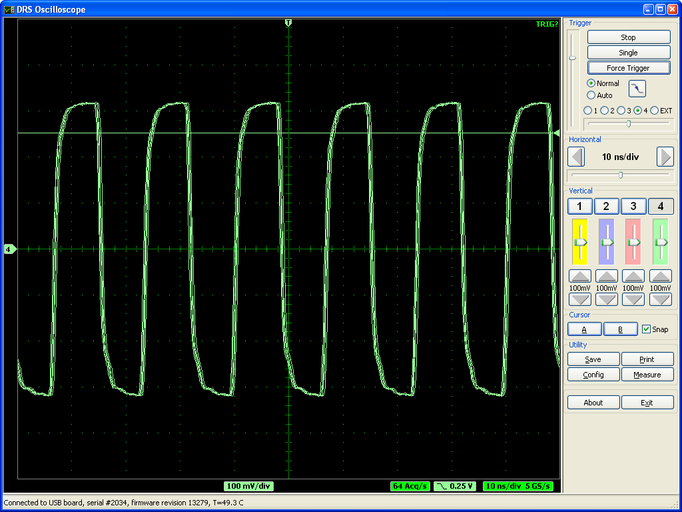
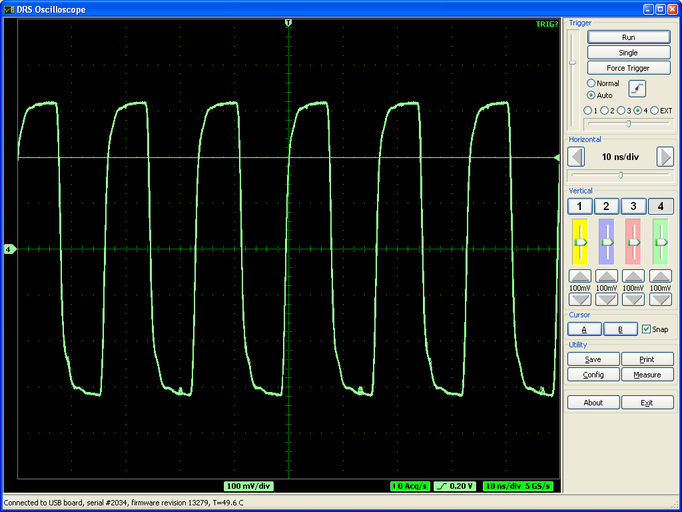
The integral temporal nonlineairy at 5 GSPS before timing calibration is about 600 ps as can be seen by the jitter of the overlaid waveforms.
In order to do a timing calibration, the firmware revison 13297 or later is required. The current software package 2.1 contains an updated firmware, but unfortunately one needs a Xilinx download cable to flash this new firmware (see http://drs.web.psi.ch/download/ under "Software Versions"). If some people want an update but do not want to buy such a cable, we offer a free update at our institute (just the postage has to be paid). The old evaluation board (Rev. 1.0, plastic housing) can unfortunately not be updated.
After the offset calibration is made, there are small (~20mV) short spikes left. They probably come from some cross-talk between the USB interface and the analog part of the board. This is currently under investigation. If new updates become available, they will be announced in this forum.
April 27th, 2009,
Stefan Ritt |
|
584
|
Sat Jan 28 14:11:58 2017 |
Danny Petschke | AND trigger problems |
Dear Stefan,
I have 2 identical pulses as a splittet signal with an amplitude of 300mV. Range is -0.5-0.5V, 5.12GSamp using the Evaluation-Board. Both signals are triggered in AND logic. One of the signals is delayed by a fixed value of 1-50ns for testing. On increasing the trigger Level from 10% to 50% of amplitude (pulse rise time is 2.5ns) pulses cannot anymore triggered above 4-5ns delay. It means there is a proportionality between the trigger level and the available range where 2 signals can be triggered in AND logic (Time-difference between 2 pulses). Do I anything misunderstand or is the time the comparator needs by higher trigger Levels for comparation longer than the 200ns at 5.12GSamp?
Board was timing and voltage calibrated before.
Thx
Danny |
|
585
|
Mon Jan 30 16:37:33 2017 |
Stefan Ritt | AND trigger problems |
In the evaluation board we use an ADCMP601 comparator, which has a setup and hold time of 4.6 ns. So a pulse which exceeds the threshold for less than 4.6 ns will not trigger the board. If you AND two signals together, an additional constraint might apply on the coincidence pulse. This is processed in the FPGA, but once it becomes too short, it won't trigger the board as well. I never made a real measurement of that, but I would not be suprised if the coicidence signal (output of AND), needs to be at least 4-5 ns wide.
If you need more refined trigger conditions, make yourself an old-fashioned external trigger (with NIM modules for example), stretch the output to 10 ns and feed it into the external trigger input of the DRS4 board (5V CMOS logic, not NIM!).
Best,
Stefan
| Danny Petschke wrote: |
|
Dear Stefan,
I have 2 identical pulses as a splittet signal with an amplitude of 300mV. Range is -0.5-0.5V, 5.12GSamp using the Evaluation-Board. Both signals are triggered in AND logic. One of the signals is delayed by a fixed value of 1-50ns for testing. On increasing the trigger Level from 10% to 50% of amplitude (pulse rise time is 2.5ns) pulses cannot anymore triggered above 4-5ns delay. It means there is a proportionality between the trigger level and the available range where 2 signals can be triggered in AND logic (Time-difference between 2 pulses). Do I anything misunderstand or is the time the comparator needs by higher trigger Levels for comparation longer than the 200ns at 5.12GSamp?
Board was timing and voltage calibrated before.
Thx
Danny
|
|
|
616
|
Thu Jun 8 14:26:23 2017 |
Rebecca Schmitz | AND Trigger problems with 2-3 channels |
Hello,
I work with the DRS4 Evaluation Board V5 and I have a problem with the software.
I have a problem with the AND trigger setting.
For this I have chosen the AND trigger function. However, when ONE channel senses an impulse, it triggers. I'm not able to see signals in the other channels, which I selected for the coincidence.
What is the cause of this? Maybe the time window?
I would like to measure a coincidence with two or three random channels. Is it possible?
Thanks for the help.
Rebecca |