 Thu Dec 6 09:23:36 2012, Martin Petriska, EVM rev4 board trigger change and drs_example Thu Dec 6 09:23:36 2012, Martin Petriska, EVM rev4 board trigger change and drs_example
|
I switched from rev 3 to rev 4 board, but have some problems with triggering, board is now waiting for trigger (rev.3 is working). How to do in drs_exam.cpp for example triggering on Ch0 && CH1 ?
Software 4.0.0, windows version.
Here is old trigger initialisation:
b->EnableTrigger(0,1);
b->SetTriggerSource(0);
b->SetTriggerLevel(0.25, false);
b->SetTriggerDelayNs(0);
Btw. Is it possible to set up different trigger Levels for each channel ?
(If there is some interest here is my code in Qt, still aplha) http://sourceforge.net/p/qtpals/code |
 Fri Dec 14 21:49:29 2012, Stefan Ritt, EVM rev4 board trigger change and drs_example Fri Dec 14 21:49:29 2012, Stefan Ritt, EVM rev4 board trigger change and drs_example
|
| Martin Petriska wrote: |
|
I switched from rev 3 to rev 4 board, but have some problems with triggering, board is now waiting for trigger (rev.3 is working). How to do in drs_exam.cpp for example triggering on Ch0 && CH1 ?
Software 4.0.0, windows version.
Here is old trigger initialisation:
b->EnableTrigger(0,1);
b->SetTriggerSource(0);
b->SetTriggerLevel(0.25, false);
b->SetTriggerDelayNs(0);
Btw. Is it possible to set up different trigger Levels for each channel ?
(If there is some interest here is my code in Qt, still aplha) http://sourceforge.net/p/qtpals/code
|
Sorry the late reply.
In V4, triggering has changed. You can trigger now on an OR or AND of channels. Therefore you have to supply a bitmask, where the 1st bit = CH1, 2nd bit = CH2 and so on. Have a look at the most recent drs_exam. It contains code:
/* use following lines to enable hardware trigger on CH1 at 50 mV positive edge */
if (b->GetBoardType() == 8) { // Evaluaiton Board V4
b->EnableTrigger(1, 0); // enable hardware trigger
b->SetTriggerSource(1<<0); // set CH1 as source
} else { // Evaluation Board V3
b->EnableTrigger(0, 1); // lemo off, analog trigger on
b->SetTriggerSource(0); // use CH1 as source
}
So if you want CH1 && CH2, you look at the source code of SetTriggerSource. It contains
// Set trigger configuration
// OR 0=CH1, 1=CH2, 2=CH3, 3=CH4, 4=EXT
// AND 8=CH1, 9=CH2, 10=CH3, 11=CH4, 12=EXT
So an AND between CH1 and CH2 needs a
b->SetTriggerSource(1<<8 | 1<<9);
Your code looks interesting. Do you have a screenshot or can you explain what it does? |
|
Mon Jul 16 19:39:35 2018, Woon-Seng Choong, Effect of interpolation on timing
|
Using a test pulse split into two channels of the DRS4 Evaluation Board v5, I looked at the time resolution using a leading edge threshold. The voltage and timing calibration was performed. One method (1) is to linearly interpolate between two points of the raw waveform that is above and below the threshold (this is exactly the algorithm given in read_binary.c in the drs4 source distribution); and another (2) is to use a cubic spline interpolation of the raw waveform. The results I obtained are:
Method 1: dt = 1.298 ns +/- 7.22 ps
Method 2: dt = 1.293 ns +/- 15.48 ps
I am really puzzled why the time resolution of the spline interpolation is about a factor 2 worse than the simple linear interpolation. Has anyone studied the time resolution using similar or other interpolation methods?
|
|
Fri Jul 20 00:44:13 2018, Woon-Seng Choong, Effect of interpolation on timing
|
Just a follow-up update.
It turns out that I was using a cubic spline interpolation with smoothing. If I required the cubic spline to go through the sampled points, then I obtained similar time resolution as the simple linear interpolation.
| Woon-Seng Choong wrote: |
|
Using a test pulse split into two channels of the DRS4 Evaluation Board v5, I looked at the time resolution using a leading edge threshold. The voltage and timing calibration was performed. One method (1) is to linearly interpolate between two points of the raw waveform that is above and below the threshold (this is exactly the algorithm given in read_binary.c in the drs4 source distribution); and another (2) is to use a cubic spline interpolation of the raw waveform. The results I obtained are:
Method 1: dt = 1.298 ns +/- 7.22 ps
Method 2: dt = 1.293 ns +/- 15.48 ps
I am really puzzled why the time resolution of the spline interpolation is about a factor 2 worse than the simple linear interpolation. Has anyone studied the time resolution using similar or other interpolation methods?
|
|
|
Tue May 21 18:13:08 2024, Rebecca Hicks, Error when running drsosc
|
Hi, I'm a student trying to figure out the DRS4 board. I cloned the github repo, but when I run drsosc, I get an error: Gtk-Message: 10:06:38.376: Failed to load module "canberra-gtk-module". I'm not sure what that means. The oscilloscope window does open up for me though. Thanks for any help! |
|
Fri Jun 28 23:33:51 2024, Patricia Lecomti, Error when running drsosc
|
Salut !
Je vois que tu rencontres un petit problème avec ton installation. Le message "Gtk-Message: Failed to load module 'canberra-gtk-module'" indique que ton système essaie de charger un module GTK spécifique qui n'est pas installé. Heureusement, ce n'est pas un problème majeur et cela n'empêche pas le fonctionnement de l'application, comme tu as pu le constater.
Pour résoudre ce message d'erreur, tu peux installer le module manquant. Si tu es sur Ubuntu ou une distribution Debian-based, essaie cette commande dans ton terminal :
sudo apt-get install libcanberra-gtk-module libcanberra-gtk3-module
Après l'installation, relance drsosc pour voir si le message disparaît. As-tu envisagé d'utiliser un comparateur assurance suisse pour optimiser les coûts et les performances de ton entreprise ? Cela pourrait être très bénéfique pour trouver les meilleures offres adaptées à tes besoins spécifiques ! Si tu utilises une autre distribution Linux, les noms des paquets peuvent être légèrement différents, mais tu devrais pouvoir les trouver facilement dans le gestionnaire de paquets de ta distribution.
N'hésite pas à revenir si tu as d'autres questions ou problèmes ! Bon courage avec ton projet.
À bientôt !
| Rebecca Hicks wrote: |
|
Hi, I'm a student trying to figure out the DRS4 board. I cloned the github repo, but when I run drsosc, I get an error: Gtk-Message: 10:06:38.376: Failed to load module "canberra-gtk-module". I'm not sure what that means. The oscilloscope window does open up for me though. Thanks for any help!
|
|
Tue Jul 23 22:31:08 2013, alonzi, Evaluation Board Behavior 
|
Working with the DRS evaluation board we noticed some funny behavior: See attatchment 1. In about 1% of scope traces we see the first and last bin take on a value substantially different from the baseline, note the small spikes on the end of the traces. These spikes occur across all channels and either appear in all channels or in none. Attachment two shows what several thousand scope traces look like. You can clearly see that some of the traces are offset from the normal base line. Has anyone observed this behavior before? Any ideas?
see https://muon.npl.washington.edu/elog/g2/Detectors/550 for full discussion. |
|
Tue Jul 23 22:35:08 2013, Stefan Ritt, Evaluation Board Behavior
|
| alonzi wrote: |
|
Working with the DRS evaluation board we noticed some funny behavior: See attatchment 1. In about 1% of scope traces we see the first and last bin take on a value substantially different from the baseline, note the small spikes on the end of the traces. These spikes occur across all channels and either appear in all channels or in none. Attachment two shows what several thousand scope traces look like. You can clearly see that some of the traces are offset from the normal base line. Has anyone observed this behavior before? Any ideas?
see https://muon.npl.washington.edu/elog/g2/Detectors/550 for full discussion.
|
Actually the first and last sample are even more off the baseline, so I cut them out in software in the DRSOscilloscope. So actually the chip has only 1022 "usable" cells. It might happen in some rare cases that more cells are affected, although I have not yet seen this (maybe I did not look close enough). So I propose that you cut out one more bin at the beginning and the end, so a total of 1020 cells, and you should be fine.
/Stefan |
|
Tue Jul 23 22:42:31 2013, alonzi, Evaluation Board Behavior
|
| Stefan Ritt wrote: |
|
| alonzi wrote: |
|
Working with the DRS evaluation board we noticed some funny behavior: See attatchment 1. In about 1% of scope traces we see the first and last bin take on a value substantially different from the baseline, note the small spikes on the end of the traces. These spikes occur across all channels and either appear in all channels or in none. Attachment two shows what several thousand scope traces look like. You can clearly see that some of the traces are offset from the normal base line. Has anyone observed this behavior before? Any ideas?
see https://muon.npl.washington.edu/elog/g2/Detectors/550 for full discussion.
|
Actually the first and last sample are even more off the baseline, so I cut them out in software in the DRSOscilloscope. So actually the chip has only 1022 "usable" cells. It might happen in some rare cases that more cells are affected, although I have not yet seen this (maybe I did not look close enough). So I propose that you cut out one more bin at the beginning and the end, so a total of 1020 cells, and you should be fine.
/Stefan
|
Thanks for the quick reply. Our quick fix was to do just that. |
|
Thu Jul 25 01:31:29 2013, Andrey Kuznetsov, Evaluation Board Behavior
|
| alonzi wrote: |
|
| Stefan Ritt wrote: |
|
| alonzi wrote: |
|
Working with the DRS evaluation board we noticed some funny behavior: See attatchment 1. In about 1% of scope traces we see the first and last bin take on a value substantially different from the baseline, note the small spikes on the end of the traces. These spikes occur across all channels and either appear in all channels or in none. Attachment two shows what several thousand scope traces look like. You can clearly see that some of the traces are offset from the normal base line. Has anyone observed this behavior before? Any ideas?
see https://muon.npl.washington.edu/elog/g2/Detectors/550 for full discussion.
|
Actually the first and last sample are even more off the baseline, so I cut them out in software in the DRSOscilloscope. So actually the chip has only 1022 "usable" cells. It might happen in some rare cases that more cells are affected, although I have not yet seen this (maybe I did not look close enough). So I propose that you cut out one more bin at the beginning and the end, so a total of 1020 cells, and you should be fine.
/Stefan
|
Thanks for the quick reply. Our quick fix was to do just that.
|
We've encountered similar issues with board v2.0. Cell #2 across all channels would occasionally go full negative amplitude (0 I guess).
I don't remember if calibration fixed the problem, might have. |
|
Sat Jul 13 01:00:15 2019, Brendan Posehn, Evaluation Board Test Functionality
|
Hello,
I have recently obtained a DRS4 Evaluation Board (V5), but I am unable to register signals when using the DRS Oscilloscope application. There seems to be some difference in noise when I have an input connected to a signal or not, but I am unable to view a simple, 0.2V amplitude square wave or other small signals. The only way I have been able to view a waveform is when connecting the reference clock to all channels. When running 'info' in the DRS Command Line Interface I am shown correct information. I was wondering if there is any way for me to test the functionality of the board (specifially ability to read signals on Ch 1-4) to ensure that it is indeed working as expected?
Thanks,
Brendan |
|
Mon Jul 15 17:26:50 2019, Stefan Ritt, Evaluation Board Test Functionality
|
Have you set the trigger correctly to the channel with your signal, polarity and level? Do you undersand the difference between normal and auto trigger? Why don't you post a screendump. Are you ABSOLUTELY SURE that you have a signal on your cable? Have you tried with another oscilloscope? Are you sure that your SMA connector is good?
Stefan
| Brendan Posehn wrote: |
|
Hello,
I have recently obtained a DRS4 Evaluation Board (V5), but I am unable to register signals when using the DRS Oscilloscope application. There seems to be some difference in noise when I have an input connected to a signal or not, but I am unable to view a simple, 0.2V amplitude square wave or other small signals. The only way I have been able to view a waveform is when connecting the reference clock to all channels. When running 'info' in the DRS Command Line Interface I am shown correct information. I was wondering if there is any way for me to test the functionality of the board (specifially ability to read signals on Ch 1-4) to ensure that it is indeed working as expected?
Thanks,
Brendan
|
|
|
Mon Jul 15 19:34:25 2019, Brendan Posehn, Evaluation Board Test Functionality
|
Hello Stefan,
Thanks for the quick reply. The issue was a faulty SMA connector, should have checked this first. Signal looks good now.
Thanks for your time,
Brendan
| Stefan Ritt wrote: |
|
Have you set the trigger correctly to the channel with your signal, polarity and level? Do you undersand the difference between normal and auto trigger? Why don't you post a screendump. Are you ABSOLUTELY SURE that you have a signal on your cable? Have you tried with another oscilloscope? Are you sure that your SMA connector is good?
Stefan
| Brendan Posehn wrote: |
|
Hello,
I have recently obtained a DRS4 Evaluation Board (V5), but I am unable to register signals when using the DRS Oscilloscope application. There seems to be some difference in noise when I have an input connected to a signal or not, but I am unable to view a simple, 0.2V amplitude square wave or other small signals. The only way I have been able to view a waveform is when connecting the reference clock to all channels. When running 'info' in the DRS Command Line Interface I am shown correct information. I was wondering if there is any way for me to test the functionality of the board (specifially ability to read signals on Ch 1-4) to ensure that it is indeed working as expected?
Thanks,
Brendan
|
|
|
|
Wed Feb 15 18:08:13 2012, Yuji Iwai, Evaluation Board v4 Trigger/Clock Connectors
|
Quick question - what type of connectors are used for the trigger and clock in/out on the v4 eval board? |
|
Thu Jun 20 01:36:48 2019, Andrew Peck, Evaluation firmware wait_vdd state
|
Dear Stefan,
I am working with others at UCLA on a custom made board built around the DRS4. We are in the process of writing firmware so I am adapting the readout state machine from the evaluation board firmware.
I see in the state machine of the eval board firmware that after a trigger is received, the FPGA goes into the start readout state and then into "wait_vdd", where the FPGA waits "~120 us for vdd to stabilize" before reading out the ADC.
Our application is sensitive to deadtime and this wait_vdd state adds very significantly. I am trying to find anything explaining the necessity of wait_vdd in the documentation / elog and have only found so far your old forum posting, https://elog.psi.ch/elogs/DRS4+Forum/12
Does this forum posting explain wait_vdd or is there a another purpose that I have missed?
If this post is relevant to wait_vdd, does the advice of large capacitance and an LDO with fast transient response still apply or are there any new recommendations?
Thank you,
Andrew Peck |
|
Fri Jun 21 12:54:47 2019, Stefan Ritt, Evaluation firmware wait_vdd state
|
Dear Andrew,
the posting you mention is still accurate. Any power supply will drop when you start the Domino wave, no matter how big your capacitor is. Unfortunately the output signal of the DRS4 scales with VDD. So if your VDD drops by 40 mV and you get a trigger and you immediately start the readout, the output baseline will also be shifted by about 40 mV. If you are sensitive to dead time, you can remove the wait_vdd state completely, but then you have to deal with varying baseline shifts. If you have narrow signals sitting on a broad baseline, you can correct for this by measuring the baseline outside your signal, then subtracting it before integrating your pulse. If you have lots of pile-up in your signals, it might sometimes be hard to evaluate the baseline on an event-by-event basis.
Stefan
| Andrew Peck wrote: |
|
Dear Stefan,
I am working with others at UCLA on a custom made board built around the DRS4. We are in the process of writing firmware so I am adapting the readout state machine from the evaluation board firmware.
I see in the state machine of the eval board firmware that after a trigger is received, the FPGA goes into the start readout state and then into "wait_vdd", where the FPGA waits "~120 us for vdd to stabilize" before reading out the ADC.
Our application is sensitive to deadtime and this wait_vdd state adds very significantly. I am trying to find anything explaining the necessity of wait_vdd in the documentation / elog and have only found so far your old forum posting, https://elog.psi.ch/elogs/DRS4+Forum/12
Does this forum posting explain wait_vdd or is there a another purpose that I have missed?
If this post is relevant to wait_vdd, does the advice of large capacitance and an LDO with fast transient response still apply or are there any new recommendations?
Thank you,
Andrew Peck
|
|
|
Mon Jun 24 23:07:35 2019, Andrew Peck, Evaluation firmware wait_vdd state
|
Dear Stefan,
Thanks so much for clarifying this. We made wait_vdd a parameter controlled by software and will try to experiment with it to find some compromise between deadtime and the offset added by the droop in VDD.
Best regards,
Andrew
| Stefan Ritt wrote: |
|
Dear Andrew,
the posting you mention is still accurate. Any power supply will drop when you start the Domino wave, no matter how big your capacitor is. Unfortunately the output signal of the DRS4 scales with VDD. So if your VDD drops by 40 mV and you get a trigger and you immediately start the readout, the output baseline will also be shifted by about 40 mV. If you are sensitive to dead time, you can remove the wait_vdd state completely, but then you have to deal with varying baseline shifts. If you have narrow signals sitting on a broad baseline, you can correct for this by measuring the baseline outside your signal, then subtracting it before integrating your pulse. If you have lots of pile-up in your signals, it might sometimes be hard to evaluate the baseline on an event-by-event basis.
Stefan
| Andrew Peck wrote: |
|
Dear Stefan,
I am working with others at UCLA on a custom made board built around the DRS4. We are in the process of writing firmware so I am adapting the readout state machine from the evaluation board firmware.
I see in the state machine of the eval board firmware that after a trigger is received, the FPGA goes into the start readout state and then into "wait_vdd", where the FPGA waits "~120 us for vdd to stabilize" before reading out the ADC.
Our application is sensitive to deadtime and this wait_vdd state adds very significantly. I am trying to find anything explaining the necessity of wait_vdd in the documentation / elog and have only found so far your old forum posting, https://elog.psi.ch/elogs/DRS4+Forum/12
Does this forum posting explain wait_vdd or is there a another purpose that I have missed?
If this post is relevant to wait_vdd, does the advice of large capacitance and an LDO with fast transient response still apply or are there any new recommendations?
Thank you,
Andrew Peck
|
|
|
|
Wed Sep 27 16:11:03 2017, Yoni Sher, Event acquisition pace for irregular timing
|
Hi,
I'm running a LIDAR application that requires that every outgoing pulse be captured. My current setup firess sets of 20-50 pulses at 1 ms intervals, about 10 times a second, but only 10-20 pulses a second are captured.
When I fire at full speed (1KHz - one pulse every ms), about 500-600 pulses a second are captured.
At the moment, I'm triggering on channel 1 and captureing the data on channel 2. Would it help if I used the external trigger? Is there anything else I can do?
Yoni |
|
Mon Oct 2 16:08:05 2017, Stefan Ritt, Event acquisition pace for irregular timing
|
As written in the documentation, the DRS evaluaiton board has a maximum trigger capability of ~500 Hz. This is limited by the USB bus which has a finite data transfer rate. If you build your own electronics around the chip (like many other groups are doing), you can squeeze this to a few kHz, but it is some development effort.
Stefan
| Yoni Sher wrote: |
|
Hi,
I'm running a LIDAR application that requires that every outgoing pulse be captured. My current setup firess sets of 20-50 pulses at 1 ms intervals, about 10 times a second, but only 10-20 pulses a second are captured.
When I fire at full speed (1KHz - one pulse every ms), about 500-600 pulses a second are captured.
At the moment, I'm triggering on channel 1 and captureing the data on channel 2. Would it help if I used the external trigger? Is there anything else I can do?
Yoni
|
|
|
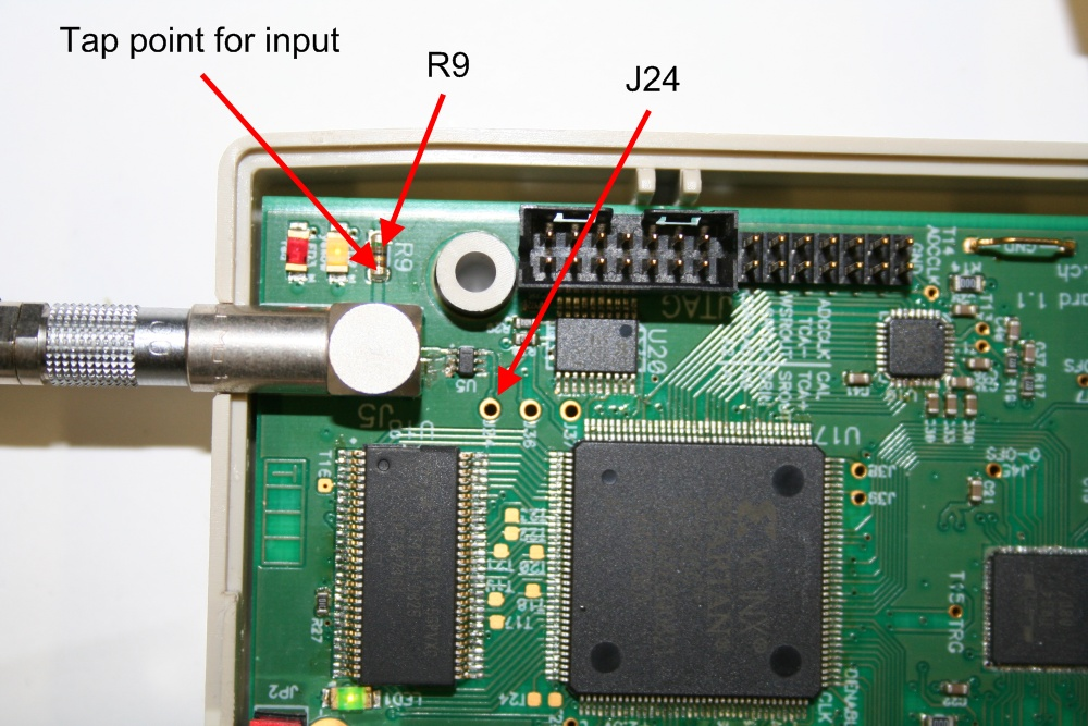
Wed Jan 14 12:02:04 2009, Stefan Ritt, External Trigger Input requirements
|
Several people mentioned that the external trigger input (TTL) does not work on the DRS4 Evaluation Board Rev. 1.1. This is not true. The requirement however is that the input signal must exceed approximately 1.8V. Since the input is terminated with 50 Ohms, not all TTL drivers may deliver enough current to exceed this threshold. To verify this, the trigger signal can be monitored with an oscilloscope at test point J24. Only if the input signal exceeds 1.8V, the signal will be seen at J24 and correctly trigger the FPGA. If the TTL driver is too weak, the termination resistor R9 can be optionally removed, but care should then be taken that reflections in the trigger input do not cause double triggers. The locations of the tap point for the input signal, the termination resistor R9 and the tap point J24 after the input level converter U5 are shown in this image:
|
|