 Fri Oct 28 15:51:59 2016, Stefan Ritt, Problems with DRS command line Fri Oct 28 15:51:59 2016, Stefan Ritt, Problems with DRS command line
|
No, I absolutely have no idea. Both DRSOsc and drscl use exaclty the same code to access USB.
Stefan
| Simon Mendisch wrote: |
that means, I am the second one experiencing this problem. To be more specific, the "No DRS Board found" problem is only present at one machine running Win7x64.
DRSOsc, of course not running simultaneously works just fine. Only drscl shows this behavior. Upgrading to a newer software version or a re-installation of the old one didn't solve the issue.
On other Win7x64 machines everything works fine, so I am pretty sure the problem is on this specific machine. Do you have any idea what could be the cause of this behavior?
|
|
 Fri Dec 20 20:35:31 2024, Matias Henriquez, Problem with C++ script to use DRS4 evaluation board. Not taking data. Fri Dec 20 20:35:31 2024, Matias Henriquez, Problem with C++ script to use DRS4 evaluation board. Not taking data. 
|
Hello,
I need to write a script in C++ to take data using the DRS4 evaluation board v4. For that, I used the drs_exam.cpp example as a reference. This is my code (see attachement 2), which is very similar to the provided example, however the difference is that I need to trigger on CH1 OR CH2. In the next version I will need to trigger with an OR in all channels.
The problem is, my code gets stuck in waiting for trigger or only 1 event occurs (event 0). I read that event and it doesn't even go above 30mV, which was the threshold I set. There are some questions I have:
- Why Transparent mode is activated for Hardware Trigger?
- Why EnableTCal is activated? is the drs4_exam example based acquires the 100MHz reference just for the sake of the example? or is just a time calibration routine?
- Can someone explain the function EnableTrigger(flag1,flag2) in boardType 8? it si not clear to me how the trigger is enabled.
- To check that my input signals are correct, I run the drsosc application and I can see the signals with no problem (see attachement 1). However I noticed that I had to configure the trigger delay in the drsosc application, and I don't do that in my c++ code. I will try that later.
- How do I perform voltage calibration and time calibration using the c++ functions?
Thank you so much for your help.
|
|
Fri Dec 27 22:04:48 2024, Matias Henriquez, Problem with C++ script to use DRS4 evaluation board. Not taking data.
|
Hello, some updates:
4. I was able to capture correct waveforms using c++ code. I needed to use the function SetTriggerDelayNs() to properly capture my waveforms.
5. I noticed that the drsosc program source code uses the functions: CalibrateVolt() and CalibrateTiming() for performing calibration. For these to work, is it necessary to use EnableAcal() and EnableTcal() functions right?
I'd appreciate if you can still give some insights about 1,2 and 3. Thank you!
| Matias Henriquez wrote: |
|
Hello,
I need to write a script in C++ to take data using the DRS4 evaluation board v4. For that, I used the drs_exam.cpp example as a reference. This is my code (see attachement 2), which is very similar to the provided example, however the difference is that I need to trigger on CH1 OR CH2. In the next version I will need to trigger with an OR in all channels.
The problem is, my code gets stuck in waiting for trigger or only 1 event occurs (event 0). I read that event and it doesn't even go above 30mV, which was the threshold I set. There are some questions I have:
- Why Transparent mode is activated for Hardware Trigger?
- Why EnableTCal is activated? is the drs4_exam example based acquires the 100MHz reference just for the sake of the example? or is just a time calibration routine?
- Can someone explain the function EnableTrigger(flag1,flag2) in boardType 8? it si not clear to me how the trigger is enabled.
- To check that my input signals are correct, I run the drsosc application and I can see the signals with no problem (see attachement 1). However I noticed that I had to configure the trigger delay in the drsosc application, and I don't do that in my c++ code. I will try that later.
- How do I perform voltage calibration and time calibration using the c++ functions?
Thank you so much for your help.
|
|
|
Mon Jan 6 12:52:23 2025, Stefan Ritt, Problem with C++ script to use DRS4 evaluation board. Not taking data.
|
1. Transparent mode is not needed for the hardware trigger, no idea why the code is there. You can probably remove it.
2. EnableTCal is only for the sake of having some waveforms at the input. Indeed you have to disable it to sample real signals.
3. EnableTrigger() is there to enable the hardware trigger. The flag2 is ther for historical reasons (used in older versions of the board).
4. You figured that out already yourself.
5. The functions CalibrateVolt() and CalibrateTiming() are the ones which get called if you click on volt and time calibration in the DRSOsc application. The calibration is store on the evaluation board, so you do not have to call them in your program.
| Matias Henriquez wrote: |
|
Hello, some updates:
4. I was able to capture correct waveforms using c++ code. I needed to use the function SetTriggerDelayNs() to properly capture my waveforms.
5. I noticed that the drsosc program source code uses the functions: CalibrateVolt() and CalibrateTiming() for performing calibration. For these to work, is it necessary to use EnableAcal() and EnableTcal() functions right?
I'd appreciate if you can still give some insights about 1,2 and 3. Thank you!
| Matias Henriquez wrote: |
|
Hello,
I need to write a script in C++ to take data using the DRS4 evaluation board v4. For that, I used the drs_exam.cpp example as a reference. This is my code (see attachement 2), which is very similar to the provided example, however the difference is that I need to trigger on CH1 OR CH2. In the next version I will need to trigger with an OR in all channels.
The problem is, my code gets stuck in waiting for trigger or only 1 event occurs (event 0). I read that event and it doesn't even go above 30mV, which was the threshold I set. There are some questions I have:
- Why Transparent mode is activated for Hardware Trigger?
- Why EnableTCal is activated? is the drs4_exam example based acquires the 100MHz reference just for the sake of the example? or is just a time calibration routine?
- Can someone explain the function EnableTrigger(flag1,flag2) in boardType 8? it si not clear to me how the trigger is enabled.
- To check that my input signals are correct, I run the drsosc application and I can see the signals with no problem (see attachement 1). However I noticed that I had to configure the trigger delay in the drsosc application, and I don't do that in my c++ code. I will try that later.
- How do I perform voltage calibration and time calibration using the c++ functions?
Thank you so much for your help.
|
|
|
|
Mon Feb 15 19:43:34 2010, Ron Grazioso, Problem reading oscilloscope binary waveform output
|
I have saved some waveforms using the oscilloscope application in both binary and xml. I can see that the xml file gives me proper data values but when I try to read the binary file using IDL, it does not seem correct. This is a screen shot of the pulse I saved: 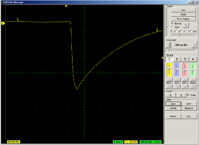
But when I open the binary file in IDL using:
data = uintarr(1024) ;unsigned integer array
readu,lun1,data
free_lun,lun1
close,lun1
;Convert bits to Volts
data=data*0.000015259-0.5
window,0,xs=512,ys=512
plot,data[*]
  I get: I get: 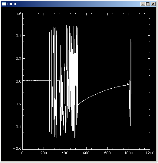
It looks like the pulse is there but there is something corrupting the data only in binary form. Is there a setting that may not be correct?
Thanks, Ron
|
|
Tue Feb 16 09:38:59 2010, Stefan Ritt, Problem reading oscilloscope binary waveform output
|
| Ron Grazioso wrote: |
|
It looks like the pulse is there but there is something corrupting the data only in binary form. Is there a setting that may not be correct?
|
Yes, but you have to recompile the oscilloscope application. Find following line in the source file DOFrame.cpp:
m_WFfd = open(filename.char_str(), O_RDWR | O_CREAT | O_TRUNC | O_TEXT, 0644);
and replace it with
m_WFfd = open(filename.char_str(), O_RDWR | O_CREAT | O_TRUNC | O_BINARY, 0644);
that fixes the problem. To compile the program, you need MS Visual C++ and you have to install the vxWidgets library. Let me know if you have any problem with that.
Anyhow I plan a major software update soon (weeks), which not only fixes this problem, but also reduces the noise considerably by doing a kind of two-fold calibration.
- Stefan |
|
Mon Jul 9 14:14:48 2012, Ivan Petrov, Problem compiling drs_exam.cpp on windows
|
Hello again. I have not got evaluation board yet, but already faced some difficulties:) I'm trying to compile drs_exam.cpp on Windows 7 using dev-c++ with imagelib-2 and WxWindows 2.4.2 DevPaks installed, but nothing works. Compile log is attached. Honestly, I'm not very familiar with c++, so any suggestions will be helpful. Thank you. |
|
Tue Jul 10 13:15:00 2012, Stefan Ritt, Problem compiling drs_exam.cpp on windows
|
| Ivan Petrov wrote: |
|
Hello again. I have not got evaluation board yet, but already faced some difficulties:) I'm trying to compile drs_exam.cpp on Windows 7 using dev-c++ with imagelib-2 and WxWindows 2.4.2 DevPaks installed, but nothing works. Compile log is attached. Honestly, I'm not very familiar with c++, so any suggestions will be helpful. Thank you.
|
I have no experience with dev-c++, so I cannot be of help here. The supported systems are Linux and Windows with MS Visual C++. But it looks like the problems are related to compiling wxWidgets, which actually you do NOT need for drs_exam.cpp. The wxWidgets library is only needed for the DRSOsc application. If you want to compile it anyhow, first learn how to compile standard WxWidgets applications from
http://www.wxwidgets.org/docs/tutorials/devcpp.htm
Best regards,
Stefan |
|
Wed Jul 11 10:04:51 2012, Ivan Petrov, Problem compiling drs_exam.cpp on windows
|
| Stefan Ritt wrote: |
|
| Ivan Petrov wrote: |
|
Hello again. I have not got evaluation board yet, but already faced some difficulties:) I'm trying to compile drs_exam.cpp on Windows 7 using dev-c++ with imagelib-2 and WxWindows 2.4.2 DevPaks installed, but nothing works. Compile log is attached. Honestly, I'm not very familiar with c++, so any suggestions will be helpful. Thank you.
|
I have no experience with dev-c++, so I cannot be of help here. The supported systems are Linux and Windows with MS Visual C++. But it looks like the problems are related to compiling wxWidgets, which actually you do NOT need for drs_exam.cpp. The wxWidgets library is only needed for the DRSOsc application. If you want to compile it anyhow, first learn how to compile standard WxWidgets applications from
http://www.wxwidgets.org/docs/tutorials/devcpp.htm
Best regards,
Stefan
|
Ok, this was my bad, I added some unnecessary files to project. Drs_exam compiles well with ms vc++. Thanks! |
|
Thu May 12 05:18:47 2016, Yu, Problem For Software Download
|
Hi
I can't download the software for windows on this website 'www.psi.ch/drs/software-download', there is some mistake when i click on download.
If convenient, can you send the software Version 5.0.5 for windows to me? My E-mail address is 'yuhaiyang421@163.com'. Thank you!
Best Regards
Yu |
|
Thu May 12 08:16:41 2016, Stefan Ritt, Problem For Software Download
|
Can you tell me (screendump) what is the problem on the web site https://www.psi.ch/drs/software-download ? It should redirect you to
https://www.dropbox.com/sh/qul1cgtm4x7zx13/AADKQ-qGQGdAHPu6OR3vTNY0a?dl=0
for the Windows download.
I cannot send executables via email, that won't go though any spam filter.
Stefan
| Yu wrote: |
|
Hi
I can't download the software for windows on this website 'www.psi.ch/drs/software-download', there is some mistake when i click on download.
If convenient, can you send the software Version 5.0.5 for windows to me? My E-mail address is 'yuhaiyang421@163.com'. Thank you!
Best Regards
Yu
|
|
|
Tue Jul 7 16:39:57 2009, Stefan Ritt, Power up problem and remedy
|
Maybe some of you have experienced that the DRS4 chip can get pretty hot after power up. After it's initialized the first time, the power consumption goes back to normal. I finally found the cause of this problem and have a remedy. Here is the new paragraph from the updated data sheet:
During power-up, care has to be taken that the DENABLE and DWRITE signals are low. If not, the domino wave can get started before the power supply voltages are stable, which brings the DRS4 chip into a state where it draws a considerable amount of current and heats up significantly. This can be problematic if the signals are directly generated by a FPGA, since most FPGAs have internal pull-up resistors which get activated during the configuration phase of the FPGA. In such a case, the DENABLE and DWRITE signals should be connected to GND with a pull down resistor. This resistor should be much smaller than the FPGA pull-up resistor in order to keep the signals close to GND during the FPGA configuration. A typical value is 4.7 kOhm.
The attached schematics shows the location of the two required resistors. |
|
Wed Nov 23 08:17:23 2016, Abhishek Rajput, Potential Incorrect Timing Calibration for DRS4 Data
|
Hello,
I was running through a particular binary file containing data taken on all 4 channels of the DRS4 and printing out the value of the first time sample for each channel (per event). While doing so, I noticed that some of these times were negative. For this dataset, channel 1 was chosen as the reference channel (which is the default setup in Stefan's DRS4 macro). From my understanding, the calibration procedure delineated in the DRS4 manual and shown in the code below is supposed to sync the timing of each channel relative to sample 0. However, this does not appear to be the case for when I print out the time value of the first sample, I notice that only channel 1's 0th sample is set to 0. The first sample for the other channels is nonzero (and most often negative).
Even more strange is when I test another 4-channel dataset with the same code, this issue does not appear. More specifically, the first time sample on each waveform on all channels is set to 0, as should be the case.
My question is therefore whether or not the timing calibration varies from dataset to dataset. My initial thought was that this should not be the case, but I have two different data sets taken on the same set of channels which give different timing calibration results. Are there any circumstances under which this behavior can happen?
for (ch=0 ; ch<5 ; ch++) {
         i = fread(hdr, sizeof(hdr), 1, f);
         if (i < 1)
            break;
         if (hdr[0] != 'C') {
            // event header found
            fseek(f, -4, SEEK_CUR);
            break;
         }
         chn_index = hdr[3] - '0' - 1;
         fread(voltage, sizeof(short), 1024, f);

         for (i=0 ; i<1024 ; i++) {
            // convert data to volts
            waveform[chn_index][i] = (voltage[i] / 65536. - 0.5);

            // calculate time for this cell
            for (j=0,time[chn_index][i]=0 ; j<i ; j++)
              time[chn_index][i] += bin_width[chn_index][(j+eh.trigger_cell) % 1024];
         }
      }

      // align cell #0 of all channels
      t1 = time[0][(1024-eh.trigger_cell) % 1024];
      for (ch=1 ; ch<4 ; ch++) {
         t2 = time[ch][(1024-eh.trigger_cell) % 1024];
         dt = t1 - t2;
         for (i=0 ; i<1024 ; i++)
            time[ch][i] += dt;
} |
|
Thu Nov 24 13:24:26 2016, Stefan Ritt, Potential Incorrect Timing Calibration for DRS4 Data
|
The code in the macro is correct. The misconception lies in the definition what "sample 0" means. Please view the attached picture. This is simplified case with a DRS chip with only 8 cells (instead of 1024). There are two events (blue and red). In the first event, the chip is stopped at trigger cell (tc) 2, in the second case at 5. Since the readout starts with the trigger cell, the first readout sample in the first event belongs to cell #2, the next one to cell #3 and so on. In the second (red) case, the first sample belongs to cell #5, the second to cell #6 and so on. "Aligning cells 0" now means that the physical cell 0 (not the readout sample) is aligned for each channel. In the first event, the 7th readout sample will have the same time in all channels, in the second event the fourth readout cells will have the same time. This is because physical cell #0 is always at different places inside the readout array.
Stefan
| Abhishek Rajput wrote: |
|
Hello,
I was running through a particular binary file containing data taken on all 4 channels of the DRS4 and printing out the value of the first time sample for each channel (per event). While doing so, I noticed that some of these times were negative. For this dataset, channel 1 was chosen as the reference channel (which is the default setup in Stefan's DRS4 macro). From my understanding, the calibration procedure delineated in the DRS4 manual and shown in the code below is supposed to sync the timing of each channel relative to sample 0. However, this does not appear to be the case for when I print out the time value of the first sample, I notice that only channel 1's 0th sample is set to 0. The first sample for the other channels is nonzero (and most often negative).
Even more strange is when I test another 4-channel dataset with the same code, this issue does not appear. More specifically, the first time sample on each waveform on all channels is set to 0, as should be the case.
My question is therefore whether or not the timing calibration varies from dataset to dataset. My initial thought was that this should not be the case, but I have two different data sets taken on the same set of channels which give different timing calibration results. Are there any circumstances under which this behavior can happen?
for (ch=0 ; ch<5 ; ch++) {
         i = fread(hdr, sizeof(hdr), 1, f);
         if (i < 1)
            break;
         if (hdr[0] != 'C') {
            // event header found
            fseek(f, -4, SEEK_CUR);
            break;
         }
         chn_index = hdr[3] - '0' - 1;
         fread(voltage, sizeof(short), 1024, f);

         for (i=0 ; i<1024 ; i++) {
            // convert data to volts
            waveform[chn_index][i] = (voltage[i] / 65536. - 0.5);

            // calculate time for this cell
            for (j=0,time[chn_index][i]=0 ; j<i ; j++)
              time[chn_index][i] += bin_width[chn_index][(j+eh.trigger_cell) % 1024];
         }
      }

      // align cell #0 of all channels
      t1 = time[0][(1024-eh.trigger_cell) % 1024];
      for (ch=1 ; ch<4 ; ch++) {
         t2 = time[ch][(1024-eh.trigger_cell) % 1024];
         dt = t1 - t2;
         for (i=0 ; i<1024 ; i++)
            time[ch][i] += dt;
      }
|
|
|
Tue Nov 29 23:19:06 2016, Abhishek Rajput, Potential Incorrect Timing Calibration for DRS4 Data
|
Hello Stefan,
Thank you for the excellent explanation and diagram. This part of the code is now much clearer to me.
My other questions pertain to the "trigger cell". Firstly, what precisely does this mean? Moreover, how does the "trigger cell" relate to the trigger time delay we can set in the DRS4 application? This is causing some confusion for me, because regardless of where you set the trigger time delay on the DRS4 application, there are still points on the waveform that are saved prior to the moment in time when a pulse exceeds some voltage threshold we set in the application. I get the impression that "trigger delay" and "trigger cell" are unrelated concepts, so any clarification you can provide would be greatly appreciated.
Abhishek
| Stefan Ritt wrote: |
|
The code in the macro is correct. The misconception lies in the definition what "sample 0" means. Please view the attached picture. This is simplified case with a DRS chip with only 8 cells (instead of 1024). There are two events (blue and red). In the first event, the chip is stopped at trigger cell (tc) 2, in the second case at 5. Since the readout starts with the trigger cell, the first readout sample in the first event belongs to cell #2, the next one to cell #3 and so on. In the second (red) case, the first sample belongs to cell #5, the second to cell #6 and so on. "Aligning cells 0" now means that the physical cell 0 (not the readout sample) is aligned for each channel. In the first event, the 7th readout sample will have the same time in all channels, in the second event the fourth readout cells will have the same time. This is because physical cell #0 is always at different places inside the readout array.
Stefan
| Abhishek Rajput wrote: |
|
Hello,
I was running through a particular binary file containing data taken on all 4 channels of the DRS4 and printing out the value of the first time sample for each channel (per event). While doing so, I noticed that some of these times were negative. For this dataset, channel 1 was chosen as the reference channel (which is the default setup in Stefan's DRS4 macro). From my understanding, the calibration procedure delineated in the DRS4 manual and shown in the code below is supposed to sync the timing of each channel relative to sample 0. However, this does not appear to be the case for when I print out the time value of the first sample, I notice that only channel 1's 0th sample is set to 0. The first sample for the other channels is nonzero (and most often negative).
Even more strange is when I test another 4-channel dataset with the same code, this issue does not appear. More specifically, the first time sample on each waveform on all channels is set to 0, as should be the case.
My question is therefore whether or not the timing calibration varies from dataset to dataset. My initial thought was that this should not be the case, but I have two different data sets taken on the same set of channels which give different timing calibration results. Are there any circumstances under which this behavior can happen?
for (ch=0 ; ch<5 ; ch++) {
         i = fread(hdr, sizeof(hdr), 1, f);
         if (i < 1)
            break;
         if (hdr[0] != 'C') {
            // event header found
            fseek(f, -4, SEEK_CUR);
            break;
         }
         chn_index = hdr[3] - '0' - 1;
         fread(voltage, sizeof(short), 1024, f);

         for (i=0 ; i<1024 ; i++) {
            // convert data to volts
            waveform[chn_index][i] = (voltage[i] / 65536. - 0.5);

            // calculate time for this cell
            for (j=0,time[chn_index][i]=0 ; j<i ; j++)
              time[chn_index][i] += bin_width[chn_index][(j+eh.trigger_cell) % 1024];
         }
      }

      // align cell #0 of all channels
      t1 = time[0][(1024-eh.trigger_cell) % 1024];
      for (ch=1 ; ch<4 ; ch++) {
         t2 = time[ch][(1024-eh.trigger_cell) % 1024];
         dt = t1 - t2;
         for (i=0 ; i<1024 ; i++)
            time[ch][i] += dt;
      }
|
|
|
|
Wed Nov 30 08:53:58 2016, Stefan Ritt, Potential Incorrect Timing Calibration for DRS4 Data
|
The inverter chain in the DRS4 is continously running in a ring. Once you get a trigger, it is stopped. This happens in any of the 1024 cells. The last cell which sampled a signal plus ne is called "trigger cell". In the previous diagram in event #1, the last cell sampling was "1", so the trigger cell is "2". In event 2 (red case), the trigger cell is 5. If you would run like this, you see only the part of the waveform BEFORE your trigger (since the DRS4 is continously sampling and is stopped with the trigger). In order to see the full peak of your waveform, you can apply some external trigger to shift the trigger position to the right. This is done in the FPGA reading out the DRS4 chip. If your peak is let's say 20 ns wide, and you delay your trigger by 30 ns, you see the peak plus 10 ns right of the peak.
Stefan
| Abhishek Rajput wrote: |
|
Hello Stefan,
Thank you for the excellent explanation and diagram. This part of the code is now much clearer to me.
My other questions pertain to the "trigger cell". Firstly, what precisely does this mean? Moreover, how does the "trigger cell" relate to the trigger time delay we can set in the DRS4 application? This is causing some confusion for me, because regardless of where you set the trigger time delay on the DRS4 application, there are still points on the waveform that are saved prior to the moment in time when a pulse exceeds some voltage threshold we set in the application. I get the impression that "trigger delay" and "trigger cell" are unrelated concepts, so any clarification you can provide would be greatly appreciated.
Abhishek
|
|
|
Fri Dec 9 04:17:46 2016, Abhishek Rajput, Potential Incorrect Timing Calibration for DRS4 Data
|
Hello Stefan,
Many thanks for the explanations. You've cleared my confusion in this matter.
Abhishek Rajput
| Stefan Ritt wrote: |
|
The inverter chain in the DRS4 is continously running in a ring. Once you get a trigger, it is stopped. This happens in any of the 1024 cells. The last cell which sampled a signal plus ne is called "trigger cell". In the previous diagram in event #1, the last cell sampling was "1", so the trigger cell is "2". In event 2 (red case), the trigger cell is 5. If you would run like this, you see only the part of the waveform BEFORE your trigger (since the DRS4 is continously sampling and is stopped with the trigger). In order to see the full peak of your waveform, you can apply some external trigger to shift the trigger position to the right. This is done in the FPGA reading out the DRS4 chip. If your peak is let's say 20 ns wide, and you delay your trigger by 30 ns, you see the peak plus 10 ns right of the peak.
Stefan
| Abhishek Rajput wrote: |
|
Hello Stefan,
Thank you for the excellent explanation and diagram. This part of the code is now much clearer to me.
My other questions pertain to the "trigger cell". Firstly, what precisely does this mean? Moreover, how does the "trigger cell" relate to the trigger time delay we can set in the DRS4 application? This is causing some confusion for me, because regardless of where you set the trigger time delay on the DRS4 application, there are still points on the waveform that are saved prior to the moment in time when a pulse exceeds some voltage threshold we set in the application. I get the impression that "trigger delay" and "trigger cell" are unrelated concepts, so any clarification you can provide would be greatly appreciated.
Abhishek
|
|
|
|
Mon Nov 5 17:17:08 2018, Sean Quinn, Pi attenuator on eval board inputs?
|
Dear DRS4 team,
I am curious about this part of the circuit:
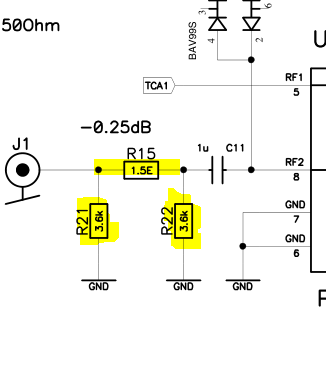
What is the purpose of this? |
|
Thu Nov 8 09:57:26 2018, Stefan Ritt, Pi attenuator on eval board inputs?
|
The attenuator compensates for the gain of the buffer which is slightly above one. In addition, it serves as a "placeholder" in case one wants larger input signals. One can easily convert the attenuator to -6db, -12db, etc. by chaning the resistors.
Stefan
| Sean Quinn wrote: |
|
Dear DRS4 team,
I am curious about this part of the circuit:
What is the purpose of this?
|
|
|
Sun Oct 23 23:32:28 2011, Hao Huan, Phase Shift for ADC Readout
|
Dear Dr. Ritt,
In the DRS 4 datasheet it is recommended to sample the analog output of the chip after 8~10 ns of the SRCLK edge for it to stablize and thus a phase shift between SRCLK and the ADC sampling clock is necessary. However in the latest version of the evaluation board firmware the phase-shifted clock was generated but not really used for the ADC interface. Is there any reason for that? |
|