| ID |
Date |
Author |
Subject |
|
31
|
Sun Jan 31 23:52:15 2010 |
Hao Huan | Failure In Flashing Xilinx PROM | Hi Stefan,
I have an old-version DRS4 evaluation board which doesn't have the latest firmware. I tried to flash the drs_eval1.ipf boundary scan chain into the XCF02S PROM with Xilinx IMPACT, and the firmware seemed to go through into the PROM. However, when I started the DRS command line interface to test the firmware it kept on reporting errors like
musb_write: requested 10, wrote -116, errno 0 (No error)
musb_read error -116
musb_write: requested 10, wrote -22, error 0 (No error)
musb_read error -116
and so on. Finally the program made a dumb recognition of the board as
Found mezz. board 0 on USB, serial #0, firmware revision 0
Do you have any idea which caused this problem? Thanks! |
|
32
|
Mon Feb 1 08:30:42 2010 |
Stefan Ritt | Failure In Flashing Xilinx PROM |
| Hao Huan wrote: |
|
Hi Stefan,
I have an old-version DRS4 evaluation board which doesn't have the latest firmware. I tried to flash the drs_eval1.ipf boundary scan chain into the XCF02S PROM with Xilinx IMPACT, and the firmware seemed to go through into the PROM. However, when I started the DRS command line interface to test the firmware it kept on reporting errors like
musb_write: requested 10, wrote -116, errno 0 (No error)
musb_read error -116
musb_write: requested 10, wrote -22, error 0 (No error)
musb_read error -116
and so on. Finally the program made a dumb recognition of the board as
Found mezz. board 0 on USB, serial #0, firmware revision 0
Do you have any idea which caused this problem? Thanks!
|
A firmware update requires a power cycle of the evaluation board. Have you tried that? I attached for you reference the current drs_eval1.mcs file, which is meant to go into the XCF02S PROM. There were recent changes also in the DRS library, and I'm not sure if yous if recent enough. So I put also the current C files which go with the firmware. They contain also some improvements which should reduce the intrinsic noise of the board. |
| Attachment 1: DRS.cpp
|
/********************************************************************

  Name:         DRS.cpp
  Created by:   Stefan Ritt, Matthias Schneebeli

  Contents:     Library functions for DRS mezzanine and USB boards

  $Id: DRS.cpp 14602 2009-11-27 11:47:36Z ritt $

\********************************************************************/

#include <stdio.h>
#include <math.h>
#include <string.h>
#include <stdlib.h>
#include <time.h>
#include <assert.h>
#include <algorithm>
#include <sys/stat.h>
#include "strlcpy.h"

#ifdef _MSC_VER
#pragma warning(disable:4996)
#   include <windows.h>
#   include <direct.h>
#else
#   include <unistd.h>
#   include <sys/time.h>
inline void Sleep(useconds_t x)
{
   usleep(x * 1000);
}
#endif

#ifdef _MSC_VER
#include <conio.h>
#define drs_kbhit() kbhit()
#else
#include <sys/ioctl.h>
int drs_kbhit()
{
   int n;

   ioctl(0, FIONREAD, &n);
   return (n > 0);
}
static inline int getch()
{
   return getchar();
}
#endif

#include <DRS.h>

#ifdef _MSC_VER
extern "C" {
#endif

#include <mxml.h>

#ifdef _MSC_VER
}
#endif

/*---- minimal FPGA firmvare version required for this library -----*/
const int REQUIRED_FIRMWARE_VERSION_DRS2 = 5268;
const int REQUIRED_FIRMWARE_VERSION_DRS3 = 6981;
const int REQUIRED_FIRMWARE_VERSION_DRS4 = 13191;

/*---- calibration methods to be stored in EEPROMs -----------------*/

#define VCALIB_METHOD  1
#define TCALIB_METHOD  1

/*---- VME addresses -----------------------------------------------*/
#ifdef HAVE_VME
/* assuming following DIP Switch settings:

   SW1-1: 1 (off)       use geographical addressing (1=left, 21=right)
   SW1-2: 1 (off)       \
   SW1-3: 1 (off)        >  VME_WINSIZE = 8MB, subwindow = 1MB
   SW1-4: 0 (on)        /
   SW1-5: 0 (on)        reserverd
   SW1-6: 0 (on)        reserverd
   SW1-7: 0 (on)        reserverd
   SW1-8: 0 (on)       \
                        |
   SW2-1: 0 (on)        |
   SW2-2: 0 (on)        |
   SW2-3: 0 (on)        |
   SW2-4: 0 (on)        > VME_ADDR_OFFSET = 0
   SW2-5: 0 (on)        |
   SW2-6: 0 (on)        |
   SW2-7: 0 (on)        |
   SW2-8: 0 (on)       /

   which gives
     VME base address = SlotNo * VME_WINSIZE + VME_ADDR_OFFSET
                      = SlotNo * 0x80'0000
*/
#define GEVPC_BASE_ADDR           0x00000000
#define GEVPC_WINSIZE               0x800000
#define GEVPC_USER_FPGA   (GEVPC_WINSIZE*2/8)
#define PMC1_OFFSET                  0x00000
#define PMC2_OFFSET                  0x80000
#define PMC_CTRL_OFFSET              0x00000    /* all registers 32 bit */
#define PMC_STATUS_OFFSET            0x10000
#define PMC_FIFO_OFFSET              0x20000
#define PMC_RAM_OFFSET               0x40000
#endif                          // HAVE_VME
/*---- USB addresses -----------------------------------------------*/
#define USB_TIMEOUT                     1000    // one second
#ifdef HAVE_USB
#define USB_CTRL_OFFSET                 0x00    /* all registers 32 bit */
#define USB_STATUS_OFFSET               0x40
#define USB_RAM_OFFSET                  0x80
#define USB_CMD_IDENT                      0    // Query identification
#define USB_CMD_ADDR                       1    // Address cycle
#define USB_CMD_READ                       2    // "VME" read <addr><size>
#define USB_CMD_WRITE                      3    // "VME" write <addr><size>
#define USB_CMD_READ12                     4    // 12-bit read <LSB><MSB>
#define USB_CMD_WRITE12                    5    // 12-bit write <LSB><MSB>

#define USB2_CMD_READ                      1
#define USB2_CMD_WRITE                     2
#define USB2_CTRL_OFFSET             0x00000    /* all registers 32 bit */
#define USB2_STATUS_OFFSET           0x10000
#define USB2_FIFO_OFFSET             0x20000
#define USB2_RAM_OFFSET              0x40000
#endif                          // HAVE_USB

/*------------------------------------------------------------------*/

using namespace std;

#ifdef HAVE_USB
#define USB2_BUFFER_SIZE (1024*1024+10)
unsigned char static *usb2_buffer = NULL;
#endif

/*------------------------------------------------------------------*/

DRS::DRS()
:  fNumberOfBoards(0)
#ifdef HAVE_VME
    , fVmeInterface(0)
#endif
{
#ifdef HAVE_USB
   MUSB_INTERFACE *usb_interface;
#endif

#if defined(HAVE_VME) || defined(HAVE_USB)
   int index = 0, i = 0;
#endif

   memset(fError, 0, sizeof(fError));

#ifdef HAVE_VME
   unsigned short type, fw, magic, serial, temperature;
   mvme_addr_t addr;

   if (mvme_open(&fVmeInterface, 0) == MVME_SUCCESS) {

      mvme_set_am(fVmeInterface, MVME_AM_A32);
      mvme_set_dmode(fVmeInterface, MVME_DMODE_D16);

      /* check all VME slave slots */
      for (index = 2; index <= 21; index++) {

         /* check PMC1 */
         addr = GEVPC_BASE_ADDR + index * GEVPC_WINSIZE;        // VME board base address
         addr += GEVPC_USER_FPGA;       // UsrFPGA base address
         addr += PMC1_OFFSET;   // PMC1 offset

         mvme_set_dmode(fVmeInterface, MVME_DMODE_D16);
         i = mvme_read(fVmeInterface, &magic, addr + PMC_STATUS_OFFSET + REG_MAGIC, 2);
         if (i == 2) {
            if (magic != 0xC0DE) {
               printf("Found old firmware, please upgrade immediately!\n");
               fBoard[fNumberOfBoards] = new DRSBoard(fVmeInterface, addr, (index - 2) << 1);
               fNumberOfBoards++;
            } else {

               /* read board type */
               mvme_read(fVmeInterface, &type, addr + PMC_STATUS_OFFSET + REG_BOARD_TYPE, 2);
               type &= 0xFF;
               if (type == 2 || type == 3 || type == 4) {    // DRS2 or DRS3 or DRS4

                  /* read firmware number */
                  mvme_read(fVmeInterface, &fw, addr + PMC_STATUS_OFFSET + REG_VERSION_FW, 2);

                  /* read serial number */
                  mvme_read(fVmeInterface, &serial, addr + PMC_STATUS_OFFSET + REG_SERIAL_BOARD, 2);

                  /* read temperature register to see if CMC card is present */
                  mvme_read(fVmeInterface, &temperature, addr + PMC_STATUS_OFFSET + REG_TEMPERATURE, 2);

                  /* LED blinking */
#if 0
                  do {
                     data = 0x00040000;
                     mvme_write(fVmeInterface, addr + PMC_CTRL_OFFSET + REG_CTRL, &data, sizeof(data));
                     mvme_write(fVmeInterface, addr + PMC2_OFFSET + PMC_CTRL_OFFSET + REG_CTRL, &data,
                                sizeof(data));

                     Sleep(500);

                     data = 0x00000000;
                     mvme_write(fVmeInterface, addr + PMC_CTRL_OFFSET + REG_CTRL, &data, sizeof(data));
                     mvme_write(fVmeInterface, addr + PMC2_OFFSET + PMC_CTRL_OFFSET + REG_CTRL, data,
                                sizeof(data));

                     Sleep(500);

                  } while (1);
#endif

                  if (temperature == 0xFFFF) {
                     printf("Found VME board in slot %d, fw %d, but no CMC board in upper slot\n", index, fw);
                  } else {
                     printf("Found DRS%d board %2d in upper VME slot %2d, serial #%d, firmware revision %d\n", type, fNumberOfBoards, index, serial, fw);

                     fBoard[fNumberOfBoards] = new DRSBoard(fVmeInterface, addr, (index - 2) << 1);
                     if (fBoard[fNumberOfBoards]->HasCorrectFirmware())
                        fNumberOfBoards++;
                     else
                        sprintf(fError, "Wrong firmware version: board has %d, required is %d\n",
                                fBoard[fNumberOfBoards]->GetFirmwareVersion(),
                                fBoard[fNumberOfBoards]->GetRequiredFirmwareVersion());
                  }
               }
            }
         }

         /* check PMC2 */
         addr = GEVPC_BASE_ADDR + index * GEVPC_WINSIZE;        // VME board base address
         addr += GEVPC_USER_FPGA;       // UsrFPGA base address
         addr += PMC2_OFFSET;   // PMC2 offset

         mvme_set_dmode(fVmeInterface, MVME_DMODE_D16);
         i = mvme_read(fVmeInterface, &fw, addr + PMC_STATUS_OFFSET + REG_MAGIC, 2);
         if (i == 2) {
            if (magic != 0xC0DE) {
               printf("Found old firmware, please upgrade immediately!\n");
               fBoard[fNumberOfBoards] = new DRSBoard(fVmeInterface, addr, (index - 2) << 1 | 1);
               fNumberOfBoards++;
            } else {

               /* read board type */
               mvme_read(fVmeInterface, &type, addr + PMC_STATUS_OFFSET + REG_BOARD_TYPE, 2);
               type &= 0xFF;
               if (type == 2 || type == 3 || type == 4) {    // DRS2 or DRS3 or DRS4

                  /* read firmware number */
                  mvme_read(fVmeInterface, &fw, addr + PMC_STATUS_OFFSET + REG_VERSION_FW, 2);

                  /* read serial number */
                  mvme_read(fVmeInterface, &serial, addr + PMC_STATUS_OFFSET + REG_SERIAL_BOARD, 2);

                  /* read temperature register to see if CMC card is present */
                  mvme_read(fVmeInterface, &temperature, addr + PMC_STATUS_OFFSET + REG_TEMPERATURE, 2);

                  if (temperature == 0xFFFF) {
                     printf("Found VME board in slot %d, fw %d, but no CMC board in lower slot\n", index, fw);
                  } else {
                     printf("Found DRS%d board %2d in lower VME slot %2d, serial #%d, firmware revision %d\n", type, fNumberOfBoards, index, serial, fw);

                     fBoard[fNumberOfBoards] = new DRSBoard(fVmeInterface, addr, ((index - 2) << 1) | 1);
                     if (fBoard[fNumberOfBoards]->HasCorrectFirmware())
                        fNumberOfBoards++;
                     else
                        sprintf(fError, "Wrong firmware version: board has %d, required is %d\n",
                                fBoard[fNumberOfBoards]->GetFirmwareVersion(),
                                fBoard[fNumberOfBoards]->GetRequiredFirmwareVersion());
                  }
               }
            }
         }
      }
   } else
      printf("Cannot access VME crate, check driver, power and connection\n");
#endif                          // HAVE_VME

#ifdef HAVE_USB
   unsigned char buffer[512];
   int found, one_found, usb_slot;

   one_found = 0;
   usb_slot = 0;
   for (index = 0; index < 127; index++) {
      found = 0;

      /* check for USB-Mezzanine test board */
      if (musb_open(&usb_interface, 0x10C4, 0x1175, index, 1, 0) == MUSB_SUCCESS) {

         /* check ID */
         buffer[0] = USB_CMD_IDENT;
         musb_write(usb_interface, 2, buffer, 1, USB_TIMEOUT);
... 6480 more lines ...
|
| Attachment 2: DRS.h
|
/********************************************************************
  DRS.h, S.Ritt, M. Schneebeli - PSI

  $Id: DRS.h 14473 2009-10-25 18:44:22Z sawada $

********************************************************************/
#ifndef DRS_H
#define DRS_H
#include <stdio.h>
#include <string.h>

#ifdef HAVE_LIBUSB
#   ifndef HAVE_USB
#      define HAVE_USB
#   endif
#endif

#ifdef HAVE_USB
#   include <musbstd.h>
#endif                          // HAVE_USB

#ifdef HAVE_VME
#   include <mvmestd.h>
#endif                          // HAVE_VME

/* disable "deprecated" warning */
#ifdef _MSC_VER
#pragma warning(disable: 4996)
#endif

#ifndef NULL
#define NULL 0
#endif

/* transport mode */
#define TR_VME   1
#define TR_USB   2
#define TR_USB2  3

/* address types */
#ifndef T_CTRL
#define T_CTRL   1
#define T_STATUS 2
#define T_RAM    3
#define T_FIFO   4
#endif

/*---- Register addresses ------------------------------------------*/

#define REG_CTRL                     0x00000    /* 32 bit control reg */
#define REG_DAC_OFS                  0x00004
#define REG_DAC0                     0x00004
#define REG_DAC1                     0x00006
#define REG_DAC2                     0x00008
#define REG_DAC3                     0x0000A
#define REG_DAC4                     0x0000C
#define REG_DAC5                     0x0000E
#define REG_DAC6                     0x00010
#define REG_DAC7                     0x00012
#define REG_CHANNEL_CONFIG           0x00014    // low byte
#define REG_CONFIG                   0x00014    // high byte
#define REG_CHANNEL_MODE             0x00016
#define REG_ADCCLK_PHASE             0x00016
#define REG_FREQ_SET_HI              0x00018    // DRS2
#define REG_FREQ_SET_LO              0x0001A    // DRS2
#define REG_TRG_DELAY                0x00018    // DRS4
#define REG_FREQ_SET                 0x0001A    // DRS4
#define REG_TRIG_DELAY               0x0001C
#define REG_LMK_MSB                  0x0001C    // DRS4 Mezz
#define REG_CALIB_TIMING             0x0001E    // DRS2
#define REG_EEPROM_PAGE_EVAL         0x0001E    // DRS4 Eval
#define REG_EEPROM_PAGE_MEZZ         0x0001A    // DRS4 Mezz
#define REG_LMK_LSB                  0x0001E    // DRS4 Mezz
#define REG_WARMUP                   0x00020    // DRS4 Mezz
#define REG_COOLDOWN                 0x00022    // DRS4 Mezz

#define REG_MAGIC                    0x00000
#define REG_BOARD_TYPE               0x00002
#define REG_STATUS                   0x00004
#define REG_RDAC_OFS                 0x0000E
#define REG_RDAC0                    0x00008
#define REG_STOP_CELL0               0x00008
#define REG_RDAC1                    0x0000A
#define REG_STOP_CELL1               0x0000A
#define REG_RDAC2                    0x0000C
#define REG_STOP_CELL2               0x0000C
#define REG_RDAC3                    0x0000E
#define REG_STOP_CELL3               0x0000E
#define REG_RDAC4                    0x00000
#define REG_RDAC5                    0x00002
#define REG_RDAC6                    0x00014
#define REG_RDAC7                    0x00016
#define REG_EVENTS_IN_FIFO           0x00018
#define REG_EVENT_COUNT              0x0001A
#define REG_FREQ1                    0x0001C
#define REG_FREQ2                    0x0001E
#define REG_TEMPERATURE              0x00020
#define REG_TRIGGER_BUS              0x00022
#define REG_SERIAL_BOARD             0x00024
#define REG_VERSION_FW               0x00026

/*---- Control register bit definitions ----------------------------*/

#define BIT_START_TRIG        (1<<0)    // write a "1" to start domino wave
#define BIT_REINIT_TRIG       (1<<1)    // write a "1" to stop & reset DRS
#define BIT_SOFT_TRIG         (1<<2)    // write a "1" to stop and read data to RAM
#define BIT_EEPROM_WRITE_TRIG (1<<3)    // write a "1" to write into serial EEPROM
#define BIT_EEPROM_READ_TRIG  (1<<4)    // write a "1" to read from serial EEPROM
#define BIT_AUTOSTART        (1<<16)
#define BIT_DMODE            (1<<17)    // (*DRS2*) 0: single shot, 1: circular
#define BIT_LED              (1<<18)    // 1=on, 0=blink during readout
#define BIT_TCAL_EN          (1<<19)    // switch on (1) / off (0) for 33 MHz calib signal
#define BIT_TCAL_SOURCE      (1<<20)
#define BIT_REFCLK_SOURCE    (1<<20)
#define BIT_FREQ_AUTO_ADJ    (1<<21)    // DRS2/3
#define BIT_TRANSP_MODE      (1<<21)    // DRS4
#define BIT_ENABLE_TRIGGER1  (1<<22)    // External LEMO/FP/TRBUS trigger
#define BIT_LONG_START_PULSE (1<<23)    // (*DRS2*) 0:short start pulse (>0.8GHz), 1:long start pulse (<0.8GHz)
#define BIT_READOUT_MODE     (1<<23)    // (*DRS3*,*DRS4*) 0:start from first bin, 1:start from domino stop
#define BIT_DELAYED_START    (1<<24)    // DRS2: start domino wave 400ns after soft trigger, used for waveform
                                        // generator startup
#define BIT_NEG_TRIGGER      (1<<24)    // DRS4: use high-to-low trigger if set
#define BIT_ACAL_EN          (1<<25)    // connect DRS to inputs (0) or to DAC6 (1)
#define BIT_TRIGGER_DELAYED  (1<<26)    // select delayed trigger from trigger bus
#define BIT_ADCCLK_INVERT    (1<<26)    // invert ADC clock
#define BIT_DACTIVE          (1<<27)    // keep domino wave running during readout
#define BIT_STANDBY_MODE     (1<<28)    // put chip in standby mode
#define BIT_TR_SOURCE1       (1<<29)    // trigger source selection bits
#define BIT_TR_SOURCE2       (1<<30)    // trigger source selection bits
#define BIT_ENABLE_TRIGGER2  (1<<31)    // analog threshold (internal) trigger

/* DRS4 configuration register bit definitions */
#define BIT_CONFIG_DMODE      (1<<8)    // 0: single shot, 1: circular
#define BIT_CONFIG_PLLEN      (1<<9)    // write a "1" to enable the internal PLL
#define BIT_CONFIG_WSRLOOP   (1<<10)    // write a "1" to connect WSROUT to WSRIN internally

/*---- Status register bit definitions -----------------------------*/

#define BIT_RUNNING           (1<<0)    // one if domino wave running or readout in progress
#define BIT_NEW_FREQ1         (1<<1)    // one if new frequency measurement available
#define BIT_NEW_FREQ2         (1<<2)
#define BIT_PLL_LOCKED0       (1<<1)    // 1 if PLL has locked (DRS4 evaluation board only)
#define BIT_PLL_LOCKED1       (1<<2)    // 1 if PLL DRS4 B has locked (DRS4 mezzanine board only)
#define BIT_PLL_LOCKED2       (1<<3)    // 1 if PLL DRS4 C has locked (DRS4 mezzanine board only)
#define BIT_PLL_LOCKED3       (1<<4)    // 1 if PLL DRS4 D has locked (DRS4 mezzanine board only)
#define BIT_SERIAL_BUSY       (1<<5)    // 1 if EEPROM operation in progress
#define BIT_LMK_LOCKED        (1<<6)    // 1 if PLL of LMK chip has locked (DRS4 mezzanine board only)

enum DRSBoardConstants {
   kNumberOfChannelsMax         =   10,
   kNumberOfCalibChannelsV3     =   10,
   kNumberOfCalibChannelsV4     =    8,
   kNumberOfBins                = 1024,
   kNumberOfChipsMax            =    4,
   kFrequencyCacheSize          =   10,
   kBSplineOrder                =    4,
   kPreCaliculatedBSplines      = 1000,
   kPreCaliculatedBSplineGroups =    5,
   kNumberOfADCBins             = 4096,
   kBSplineXMinOffset           =   20,
   kMaxNumberOfClockCycles      =  100,
};

enum DRSErrorCodes {
   kSuccess                     =  0,
   kInvalidTriggerSignal        = -1,
   kWrongChannelOrChip          = -2,
   kInvalidTransport            = -3,
   kZeroSuppression             = -4,
   kWaveNotAvailable            = -5
};

/*---- callback class ----*/

class DRSCallback
{
public:
   virtual void Progress(int value) = 0;
   virtual ~DRSCallback() {};
};

/*------------------------*/

class DRSBoard;

class ResponseCalibration {
protected:

   class CalibrationData {
   public:
      class CalibrationDataChannel {
      public:
         unsigned char   fLimitGroup[kNumberOfBins];           //!
         float           fMin[kNumberOfBins];                  //!
         float           fRange[kNumberOfBins];                //!
         short           fOffset[kNumberOfBins];               //!
         short           fGain[kNumberOfBins];                 //!
         unsigned short  fOffsetADC[kNumberOfBins];            //!
         short          *fData[kNumberOfBins];                 //!
         unsigned char  *fLookUp[kNumberOfBins];               //!
         unsigned short  fLookUpOffset[kNumberOfBins];         //!
         unsigned char   fNumberOfLookUpPoints[kNumberOfBins]; //!
         float          *fTempData;                            //!

      private:
         CalibrationDataChannel(const CalibrationDataChannel &c);              // not implemented
         CalibrationDataChannel &operator=(const CalibrationDataChannel &rhs); // not implemented

      public:
         CalibrationDataChannel(int numberOfGridPoints)
         :fTempData(new float[numberOfGridPoints]) {
            int i;
            for (i = 0; i < kNumberOfBins; i++) {
               fData[i] = new short[numberOfGridPoints];
            }
            memset(fLimitGroup,           0, sizeof(fLimitGroup));
            memset(fMin,                  0, sizeof(fMin));
            memset(fRange,                0, sizeof(fRange));
            memset(fOffset,               0, sizeof(fOffset));
            memset(fGain,                 0, sizeof(fGain));
            memset(fOffsetADC,            0, sizeof(fOffsetADC));
            memset(fLookUp,               0, sizeof(fLookUp));
            memset(fLookUpOffset,         0, sizeof(fLookUpOffset));
            memset(fNumberOfLookUpPoints, 0, sizeof(fNumberOfLookUpPoints));
         }
         ~CalibrationDataChannel() {
            int i;
            delete fTempData;
            for (i = 0; i < kNumberOfBins; i++) {
               delete fData[i];
               delete fLookUp[i];
            }
         }
      };

      bool                    fRead;                                  //!
      CalibrationDataChannel *fChannel[10];                           //!
      unsigned char           fNumberOfGridPoints;                    //!
      int                     fHasOffsetCalibration;                  //!
      float                   fStartTemperature;                      //!
      float                   fEndTemperature;                        //!
      int                    *fBSplineOffsetLookUp[kNumberOfADCBins]; //!
      float                 **fBSplineLookUp[kNumberOfADCBins];       //!
      float                   fMin;                                   //!
      float                   fMax;                                   //!
      unsigned char           fNumberOfLimitGroups;                   //!
      static float            fIntRevers[2 * kBSplineOrder - 2];

   private:
      CalibrationData(const CalibrationData &c);              // not implemented
      CalibrationData &operator=(const CalibrationData &rhs); // not implemented

   public:
      CalibrationData(int numberOfGridPoints);
      ~CalibrationData();
      static int CalculateBSpline(int nGrid, float value, float *bsplines);
      void       PreCalculateBSpline();
      void       DeletePreCalculatedBSpline();
   };

   // General Fields
   DRSBoard        *fBoard;

   double           fPrecision;

   // Fields for creating the Calibration
   bool             fInitialized;
   bool             fRecorded;
   bool             fFitted;
   bool             fOffset;
   bool             fCalibrationValid[2];

   int              fNumberOfPointsLowVolt;
   int              fNumberOfPoints;
   int              fNumberOfMode2Bins;
   int              fNumberOfSamples;
   int              fNumberOfGridPoints;
   int              fNumberOfXConstPoints;
   int              fNumberOfXConstGridPoints;
   double           fTriggerFrequency;
   int              fShowStatistics;
   FILE            *fCalibFile;

   int              fCurrentLowVoltPoint;
   int              fCurrentPoint;
   int              fCurrentSample;
   int              fCurrentFitChannel;
   int              fCurrentFitBin;

   float           *fResponseX[10][kNumberOfBins];
   float           *fResponseY;
   unsigned short **fWaveFormMode3[10];
   unsigned short **fWaveFormMode2[10];
   short          **fWaveFormOffset[10];
   unsigned short **fWaveFormOffsetADC[10];
   unsigned short  *fSamples;
   int             *fSampleUsed;

   float           *fPntX[2];
   float           *fPntY[2];
... 559 more lines ...
|
| Attachment 3: drs4_eval1.mcs
|
:020000040000FA
:10000000FFFFFFFF5599AA660C000180000000E089
:100010000C800680000000220C8004800200FCA7F7
:100020000C800380808203C90C0003800000000064
:100030000C000180000000900C0004800000000013
:100040000C000180000000800C0002000A00F30098
:1000500000000000000000000000000000000000A0
:100060000000000000000000000000000000000090
:100070000000000000000000000000000000000080
:100080000000000000000000000000000000000070
:100090000000000000000000000000000000000060
:1000A0000000000000000000000000000000000050
:1000B0000000000000000000000000000000000040
:1000C0000000000000000000000000000000000030
:1000D00000000000000009000000000000B0020065
:1000E0000000000000000000000000000000000010
:1000F0000000000000000000000000000000000000
:1001000000000000000000000000000000000000EF
:1001100000000000000000000000000000000000DF
:1001200000000000000000000000000000000000CF
:1001300000000000000000000000000000000000BF
:1001400000000000000000000000000000000000AF
:10015000000000000000000000000000000000009F
:10016000000000000000000000000000000000008F
:10017000000000000000000000000000000000007F
:10018000000000000000000000000000000000006F
:10019000000000000000000000000000000000005F
:1001A000000000000000000000000000000000004F
:1001B000000000000000000000000000000000003F
:1001C000000000000000000000000000000000002F
:1001D000000000000000000000000000000000001F
:1001E00000000000000000000040090000000000C6
:1001F000009202000000000000000000000000006B
:1002000000000000000000000000000000000000EE
:1002100000000000000000000000000000000000DE
:1002200000000000000000000000000000000000CE
:1002300000000000000000000000000000000000BE
:1002400000000000000000000000000000000000AE
:10025000000000000000000000000000000000009E
:10026000000000000000000000000000000000008E
:1002700000000000000000000000000800200070E6
:10028000000000000000000000000000000000006E
:10029000000000000000000000000000000000005E
:1002A000000000000000000000000000000000004E
:1002B000000000000000000000000000000000003E
:1002C000000000000000000000000000000000002E
:1002D000000000000000000000000000000000001E
:1002E000000000000000000000000000000000000E
:1002F00000000000000000000000000000000000FE
:1003000000000000000000000000000000000000ED
:1003100000000000000000000000000000000000DD
:1003200000000000000000000000000000000000CD
:1003300000000000000000000000000000000000BD
:1003400000000000000000000000000000000000AD
:10035000000000000000000000000000000000009D
:10036000000000000000000000000000000000008D
:10037000000000000000000000000000000000007D
:1003800000004086280002801000C000000000002D
:10039000000000000000010C86A0053128100000BC
:1003A000000000000000000000000000000000004D
:1003B0000000000000000000000005312810010CC2
:1003C00086A005312810010C86A005312810010CEB
:1003D00086A005002810010C00A005002810010CC3
:1003E00000A0050028100000000000000000000030
:1003F00000000000000000000000000000000000FD
:100400000000000000000000000000000000010CDF
:1004100000A0050028100100C6058039001000006A
:1004200000000000000000000000000000000000CC
:1004300000000000000000000000000000000000BC
:100440000000000000000100C60500000000010CD3
:1004500086A005312810010C86A005312810010C5A
:1004600086A005312810010C86A005312810000057
:10047000000000000000000000000000000000007C
:100480000000000000000000000000000000010C5F
:1004900000A005002810000000000000000000007F
:1004A000000000000000000000000000000000004C
:1004B000000000000000000000000000000000003C
:1004C000000000000000000000000000000000002C
:1004D000000000000000000000000000000000001C
:1004E000000000000000000000000000000000000C
:1004F00000000000000000000000000000000000FC
:1005000000000000000000000000000000000000EB
:1005100000000000000000000000000000000000DB
:1005200000000000000000000000000000002000AB
:1005300000000000000000000000000000000000BB
:1005400000000000000000000000000000000000AB
:10055000000000000000000000000000000000009B
:10056000000000000000000000000000000000008B
:10057000000000000000000000000000000000007B
:10058000000000000000000000000000000000006B
:10059000000000000000000000000000000000005B
:1005A000000000000000000000000000000000004B
:1005B000180400000000000000000000000000001F
:1005C00000000081000000000000000000000000AA
:1005D000000000000000000000000000000000001B
:1005E000000000800000000000000081000000000A
:1005F00000000081000000000000008100000000F9
:1006000000000081000000000000008100000000E8
:1006100000000000000000000000000000000000DA
:1006200000000000000000000000000000000000CA
:100630000000000000000000000000810000000039
:1006400000000000000000000000000000000000AA
:10065000000000000000000000000000000000009A
:10066000000000000000000000000000000000008A
:1006700000000000000000000000008100000000F9
:100680000000008100000000000000810000000068
:1006900000000081000000000000000000000000D9
:1006A000000000000000000000000000000000004A
:1006B00000000000000000000000008100000000B9
:1006C000000000000000000000000000000000002A
:1006D00000000000000004182000000000000000DE
:1006E000000000000000000000000000000000000A
:1006F00000000000000000102000000000000418AE
:100700002000000000000418200000000000041871
:1007100020000000000004182000000000000081FC
:1007200000000000000000000000000000000000C9
:1007300000000000000000000000000000000000B9
:10074000000000000000000000000000000004881D
:100750000000000000000000000000000000000099
:100760000000000000000000000000000000000089
:100770000000000000000000000000000000000079
:10078000000000000000000000000000000004184D
:1007900020000000000004182000000000000418E1
:1007A00020000000000004182000000000000000ED
:1007B0000000000000000000000000000000000039
:1007C000000000000000000000000000000004180D
:1007D00020000000000000000000000000000000F9
:1007E00000000000000000000000040020000000E5
:1007F00000000000000000000000000000000000F9
:1008000000000000000000000000000020000000C8
:100810000000040020000000000004002000000090
:1008200000000400000000000000000000000000C4
:1008300000000000000000000000000000000000B8
:1008400000000000000000000000000000000000A8
:100850000000000000000000000000000000000098
:100860000000000000000000000000002010000058
:100870000000000000000000000000000000000078
:100880000000000000000000000000000000000068
:100890000000000000000000000004000000000054
:1008A0000000040020000000000004002000000000
:1008B00000000400200000000000040020000000F0
:1008C0000000000000000000000000000000000028
:1008D0000000000000000000000000000000000018
:1008E0000000000000000000000000000000000008
:1008F0000000000000000000000000000002608115
:1009000006400000000000000000000000000000A1
:100910000000000000000000000000000000008057
:100920000640000000026081064000000002608175
:10093000064000000002608100000000000000810D
:1009400000000000000000000000000000000000A7
:100950000000000000000000000000000000000097
:100960000000000000000000000000000000000087
:100970000000000000000001000000000000000076
:100980000640000000000000000000000000000021
:100990000000000000000000000000000000000057
:1009A00000000000000000000000000000026000E5
:1009B000000000000002608106400000000260812B
:1009C00006400000000260810640000000026081D5
:1009D00006400000000000000000000000000000D1
:1009E0000000000000000000000000000000000007
:1009F0000000000000000081000000000000000076
:100A000000000000000000000000000000000000E6
:100A1000000000C39004000000000000000000007F
:100A200000000000000000000000000000000000C6
:100A3000000000C300020000000000C380050000A9
:100A4000000000C3C00C0000000000C380020000D2
:100A5000000000C090240000000000000000000022
:100A60000000000000000000000000000000000086
:100A70000000000000000000000000000000000076
:100A80000000000000000000000000C09000000016
:100A90000000000300020000000000000000000051
:100AA0000000000000000000000000000000000046
:100AB0000000000000000000000000000000000036
:100AC0000000000390000000000000C3900400003C
:100AD000000000C390020000000000C3900400006A
:100AE000000000C3900300000000000000000000B0
:100AF00000000000000000000000000000000000F6
:100B00000000000000000000000000C0900600008F
:100B100000000000000000000C00000000000000C9
:100B20000000C000000000C0002300000000000022
:100B300000000000000000000000000000000000B5
:100B400000008000000000C00022C000000000C0C3
:100B50000823C000000000C00003C000000000C067
:100B60004023C0000000004000030000000000001F
:100B70000000000000000000000000000000000075
:100B80000000000000000000000000000000000065
:100B900000000000000000000000400000000040D5
:100BA00000010000000000800022000000000000A2
:100BB0000000000000000000000000000000000035
:100BC0000000000000000000000000000000000025
:100BD00000000000000000800001C000000000C014
:100BE0000023C000000000C00023C000000000C0BF
:100BF0000023C000000000C000230000000000002F
:100C000000000000000000000000000000000000E4
:100C100000000000000000000000C00000000040D4
:100C20000023000000000000000000C00C000000D5
:100C30000000000000000000000000008000000034
:100C400000000000000000000000000000000000A4
:100C50000000000000000000000000000000000094
:100C60000000010000000000000001008000000002
:100C70000181000080000000000000000000000072
:100C80000000000000000000000000000000000064
:100C90000000000000000000000000000000000054
:100CA0000000000000000000000000000000000044
:100CB0000000000000000000000000000000000034
:100CC0000000000000000000000000000000000024
:100CD0000000000000000000000000000000000014
:100CE0000000000000000000010000000000000003
:100CF00000800000000000000080000000000000F4
:100D000000810000000000000080000000000000E2
:100D100000000000000000000000000000000000D3
:100D200000000000000000000000000000000000C3
:100D3000000000000000000000000000000000C0F3
:100D400000000000000000000000000000000200A1
:100D50008000000000000000000000000000000013
:100D6000000000000000000000000000028002807F
:100D700001000000010041000100000000004000EF
:100D800080800000400300008000000000000000A0
:100D90000000000000000000000000000000000053
:100DA0000000000000000000000000000000000043
:100DB0000000000000000000000000000000000033
:100DC0000000000000000000000000000000020021
:100DD0000100000000000000000000000000000012
:100DE0000000000000000000000000000000000003
:100DF00000000000000000000000000040000000B3
:100E000000000000020200000000000002020000DA
:100E100000000000020302000000000002020000C7
:100E200000000000000000000000000000000000C2
:100E300000000000000000000000000000000000B2
:100E400000000000000000000000000000000000A2
:100E50000000000000000000000000000000000092
:100E6000A0000000000000000000000000000000E2
:100E70000000000000000000000000000000000072
:100E80007000000000000000780000000002000078
:100E90007000000000010000A00000000001000040
:100EA00050000000000100005000000000000000A1
:100EB0000000000000000000000000000000000032
:100EC0000000000000000000000000000000000022
:100ED00000000000000000006000000000010000B1
:100EE0000000000000000000000000000000000002
:100EF00000000000000000000000000000000000F2
:100F000000000000000000000000000000000000E1
:100F1000000000000000000070000000000200005F
:100F20002800000000020000600000000000000037
:100F30007000000000000000000000000000000041
:100F400000000000000000000000000000000000A1
:100F5000000000000000000050000000000200003F
:100F60000000000000000000000000000000000081
:100F7000000000000000000020020000000000004F
:100F80000000000000000000000000000000000061
:100F90000000000000000000000000000000000051
:100FA0004000000000000000C00000000000000041
:100FB000C000000000020000C000000000020000AD
:100FC0000000000000000000000000000000000021
:100FD0000000000000000000000000000000000011
:100FE0000000000000000000000000000000000001
:100FF000C000000000000000000000000000000031
:1010000000000000000000000000000000000000E0
:1010100000000000000000000000000000000000D0
:1010200000000000000000000000000000000000C0
:101030000000000000000000200000001000000080
:10104000C000000010000000C0020000000000000E
:101050000000000000000000000000000000000090
:10106000000000000000000000000000000200007E
:101070000000000000000000000000000000000070
:1010800000000000000000008000000000000000E0
:101090000000000000000000000000000000000050
:1010A0000000000000000000C00000000000000080
:1010B00000000000040000004000000000000000EC
:1010C000800000000400000080000000000000001C
:1010D0000000000000000000000000000000000010
:1010E0000000000000000000000000000000000000
:1010F00000000000000000000000000000000000F0
:10110000400000000400000000000000000000009B
:1011100000000000000000000000000000000000CF
:1011200000000000000000000000000000000000BF
:1011300000000000000000000000000000000000AF
:10114000400000000000000000000000000000005F
:101150008000000008000000000000000000000007
:10116000000000000000000000000000000000007F
:10117000000000000000000000000000000000006F
:1011800080000000000000000000000000000000DF
:10119000000000000000000000000000000000004F
:1011A000000200000000000000000000000000003D
:1011B000000000000000000000000000000000002F
:1011C000000000000000000000000000000000001F
:1011D000000200000000000000000000000000000D
:1011E00020000000000000002000000000000000BF
:1011F00000000000000000000000000000000000EF
:1012000000000000000000000000000000000000DE
:101210000000000000000000C0000000000000000E
:1012200000000000000000000000000000000000BE
:1012300000000000000000000000000000000000AE
:10124000000000000000000000000000000000009E
:101250000000000000020000C000000000020000CA
:101260000000000000000000D000000000000000AE
:10127000000000000000000000000000000000006E
:10128000000000000000000000000000000000005E
:10129000000000000000000020000000000000002E
:1012A000000000000000000000000000000000003E
... 12981 more lines ...
|
|
797
|
Tue Sep 22 17:45:26 2020 |
Elmer Grundeman | External triggering | Dear all,
I had a question about timing jitter and external triggering.
I trigger the board externally with a 3V pulse from a DG645 delay generator and as a test I use the gated charge function to integrate another pulse of the DG which goes into channel 1 (the timing jitter between different outputs of the DG is on the order of ~25 picoseconds).
The issue I’m encountering is that the signal on channel 1 is jittering in time with ~1 ns, which means the signal is jittering with respect to my integration gate (point A and B). If I look at the data it always starts at t = 0.000 but my signal (pulse) moves around in time.
If I don’t use the external trigger but trigger on channel 1 directly the signal does not move with respect to the gate, but I can see the start and end of the trace move in time. If I look at the data the first data point is not at t = 0.000 but some other time, which jitters with ~1 ns.
I did repeat the voltage and timing calibration, but that did not help either.
Do you know where this jitter comes from and if I can get rid of it?
Best regards,
Elmer |
|
798
|
Wed Oct 7 10:56:03 2020 |
Stefan Ritt | External triggering | The trigger is there only to trigger the chip, but cannot be used as a precise time reference. If you want to measure precise timing, do this always BETWEEN two inputs, never between an input and the trigger. You might want to split and delay your trigger signal and feed one copy to another input of the evaluation board as your reference.
Stefan
| Elmer Grundeman wrote: |
|
Dear all,
I had a question about timing jitter and external triggering.
I trigger the board externally with a 3V pulse from a DG645 delay generator and as a test I use the gated charge function to integrate another pulse of the DG which goes into channel 1 (the timing jitter between different outputs of the DG is on the order of ~25 picoseconds).
The issue I’m encountering is that the signal on channel 1 is jittering in time with ~1 ns, which means the signal is jittering with respect to my integration gate (point A and B). If I look at the data it always starts at t = 0.000 but my signal (pulse) moves around in time.
If I don’t use the external trigger but trigger on channel 1 directly the signal does not move with respect to the gate, but I can see the start and end of the trace move in time. If I look at the data the first data point is not at t = 0.000 but some other time, which jitters with ~1 ns.
I did repeat the voltage and timing calibration, but that did not help either.
Do you know where this jitter comes from and if I can get rid of it?
Best regards,
Elmer
|
|
|
799
|
Wed Oct 7 11:17:52 2020 |
Elmer Grundeman | External triggering | I will try that, thanks!
| Stefan Ritt wrote: |
|
The trigger is there only to trigger the chip, but cannot be used as a precise time reference. If you want to measure precise timing, do this always BETWEEN two inputs, never between an input and the trigger. You might want to split and delay your trigger signal and feed one copy to another input of the evaluation board as your reference.
Stefan
| Elmer Grundeman wrote: |
|
Dear all,
I had a question about timing jitter and external triggering.
I trigger the board externally with a 3V pulse from a DG645 delay generator and as a test I use the gated charge function to integrate another pulse of the DG which goes into channel 1 (the timing jitter between different outputs of the DG is on the order of ~25 picoseconds).
The issue I’m encountering is that the signal on channel 1 is jittering in time with ~1 ns, which means the signal is jittering with respect to my integration gate (point A and B). If I look at the data it always starts at t = 0.000 but my signal (pulse) moves around in time.
If I don’t use the external trigger but trigger on channel 1 directly the signal does not move with respect to the gate, but I can see the start and end of the trace move in time. If I look at the data the first data point is not at t = 0.000 but some other time, which jitters with ~1 ns.
I did repeat the voltage and timing calibration, but that did not help either.
Do you know where this jitter comes from and if I can get rid of it?
Best regards,
Elmer
|
|
|
|
645
|
Tue Dec 12 00:25:50 2017 |
Diego Yankelevich | External trigger using Raspberry Pi | Dear Steffan:
We have been able to use the DRS4 using a Raspberry Pi but we have not been able to use the external trigger. What we are doing is basically comment out the code shown below (downloaded from PSI) to use the hardware trigger and uncomment the code to use the external trigger. We have not been able to get external trigger to work. Could you see what could be wrong?
Thanks
Diego
/* use following line to turn on the internal 100 MHz clock connected to all channels  */
   //b->EnableTcal(1);

   /* use following lines to enable hardware trigger on CH1 at 50 mV positive edge */

   /*
   if (b->GetBoardType() >= 8) {        // Evaluaiton Board V4&5
      b->EnableTrigger(1, 0);           // enable hardware trigger
      b->SetTriggerSource(1<<0);        // set CH1 as source
   } else if (b->GetBoardType() == 7) { // Evaluation Board V3
      b->EnableTrigger(0, 1);           // lemo off, analog trigger on
      b->SetTriggerSource(0);           // use CH1 as source
   }
   b->SetTriggerLevel(0.05);            // 0.05 V
   b->SetTriggerPolarity(false);        // positive edge
   */

   /* use following lines to set individual trigger elvels */
   //b->SetIndividualTriggerLevel(1, 0.1);
   //b->SetIndividualTriggerLevel(2, 0.2);
   //b->SetIndividualTriggerLevel(3, 0.3);
   //b->SetIndividualTriggerLevel(4, 0.4);
   //b->SetTriggerSource(15);

   b->SetTriggerDelayNs(0);             // zero ns trigger delay

   /* use following lines to enable the external trigger */
   if (b->GetBoardType() == 8) {     // Evaluaiton Board V4
      b->EnableTrigger(1, 0);           // enable hardware trigger
      b->SetTriggerSource(1<<4);        // set external trigger as source
   } else {                          // Evaluation Board V3
      b->EnableTrigger(1, 0);           // lemo on, analog trigger off
} |
|
646
|
Tue Dec 12 13:58:06 2017 |
Stefan Ritt | External trigger using Raspberry Pi | Indeed the code does not work for the current evaluation board, it has been written for a previous version and never been updated. Please use following code to enable the external trigger
/* use following lines to enable the external trigger */
if (b->GetBoardType() >= 8) { // Evaluaiton Board V4&5
b->EnableTrigger(1, 0); // enable hardware trigger
b->SetTriggerConfig(1<<4); // set external trigger as source
} else { // Evaluation Board V3
b->EnableTrigger(1, 0); // lemo on, analog trigger offf
}
Please also make sure that the signal on the external trigger input is strong enough. You need at least 2.5V at 50 Ohms, and not every driver is capable of driving 50 Ohms.
Stefan
| Diego Yankelevich wrote: |
|
Dear Steffan:
We have been able to use the DRS4 using a Raspberry Pi but we have not been able to use the external trigger. What we are doing is basically comment out the code shown below (downloaded from PSI) to use the hardware trigger and uncomment the code to use the external trigger. We have not been able to get external trigger to work. Could you see what could be wrong?
Thanks
Diego
/* use following line to turn on the internal 100 MHz clock connected to all channels  */
   //b->EnableTcal(1);

   /* use following lines to enable hardware trigger on CH1 at 50 mV positive edge */

   /*
   if (b->GetBoardType() >= 8) {        // Evaluaiton Board V4&5
      b->EnableTrigger(1, 0);           // enable hardware trigger
      b->SetTriggerSource(1<<0);        // set CH1 as source
   } else if (b->GetBoardType() == 7) { // Evaluation Board V3
      b->EnableTrigger(0, 1);           // lemo off, analog trigger on
      b->SetTriggerSource(0);           // use CH1 as source
   }
   b->SetTriggerLevel(0.05);            // 0.05 V
   b->SetTriggerPolarity(false);        // positive edge
   */

   /* use following lines to set individual trigger elvels */
   //b->SetIndividualTriggerLevel(1, 0.1);
   //b->SetIndividualTriggerLevel(2, 0.2);
   //b->SetIndividualTriggerLevel(3, 0.3);
   //b->SetIndividualTriggerLevel(4, 0.4);
   //b->SetTriggerSource(15);

   b->SetTriggerDelayNs(0);             // zero ns trigger delay

   /* use following lines to enable the external trigger */
   if (b->GetBoardType() == 8) {     // Evaluaiton Board V4
      b->EnableTrigger(1, 0);           // enable hardware trigger
      b->SetTriggerSource(1<<4);        // set external trigger as source
   } else {                          // Evaluation Board V3
      b->EnableTrigger(1, 0);           // lemo on, analog trigger off
    }
|
|
|
843
|
Tue Oct 26 10:41:46 2021 |
Mehrpad Monajem | External trigger and drs_exam | Hi Stefan,
I have two problems regarding using the drs_exam file with external trigger:
1- I connected a 200Khz signal with 20ns rising edge, 50 ohm load, and 27% duty cycle as an external trigger. The output of the drs_exam file starts from 0 to 200ns. Since I use an external trigger, I think it should be starting from 0 to 5ns and then again starting from 0. Could you please tell me where the problem is?
2- How is it possible to change from 1024 to 2048 bins in the drs_exam example?
You can find my code in the attachment.
Best regards,
Mehrpad |
|
844
|
Tue Oct 26 12:00:51 2021 |
Stefan Ritt | External trigger and drs_exam | 1. Why should your waveform start from 0 to 5ns? I don't get your point. Whenever you trigger a readout, you get a 200ns wide time window, and by definition it starts at zero.
2. In the software distribution you have a drs_exam_2048.cpp program. Note that your board needs to be physically modified before delivery to switch to 2048 bins.
Best,
Stefan
| Mehrpad Monajem wrote: |
|
Hi Stefan,
I have two problems regarding using the drs_exam file with external trigger:
1- I connected a 200Khz signal with 20ns rising edge, 50 ohm load, and 27% duty cycle as an external trigger. The output of the drs_exam file starts from 0 to 200ns. Since I use an external trigger, I think it should be starting from 0 to 5ns and then again starting from 0. Could you please tell me where the problem is?
2- How is it possible to change from 1024 to 2048 bins in the drs_exam example?
You can find my code in the attachment.
Best regards,
Mehrpad
|
|
|
846
|
Tue Oct 26 15:05:18 2021 |
Mehrpad Monajem | External trigger and drs_exam | Thanks for your reply.
1- I want to have a window size of 25.6ns instead of 200ns at 5GSPS. I have a 200khz high voltage pulser, which applies a pulse to my sample. I want to digitize the detector signal for each pulse (each pulse has a 25.6ns period). The pulser and digitizer use same 200khz trigger signal from each channel of the signal generator.
2- My DRS board has a 2048 combined stick on it. But the software distribution that I have doesn't contain the drs_exam_2048.cpp program. Could you please send the link that I can download this program? I can't find it under the link below.
link: https://www.dropbox.com/sh/clqo7ekr0ysbrip/AACoWJzrQAbf3WiBJHG89bGGa?dl=0
Best regards,
Mehrpad
| Stefan Ritt wrote: |
|
1. Why should your waveform start from 0 to 5ns? I don't get your point. Whenever you trigger a readout, you get a 200ns wide time window, and by definition it starts at zero.
2. In the software distribution you have a drs_exam_2048.cpp program. Note that your board needs to be physically modified before delivery to switch to 2048 bins.
Best,
Stefan
| Mehrpad Monajem wrote: |
|
Hi Stefan,
I have two problems regarding using the drs_exam file with external trigger:
1- I connected a 200Khz signal with 20ns rising edge, 50 ohm load, and 27% duty cycle as an external trigger. The output of the drs_exam file starts from 0 to 200ns. Since I use an external trigger, I think it should be starting from 0 to 5ns and then again starting from 0. Could you please tell me where the problem is?
2- How is it possible to change from 1024 to 2048 bins in the drs_exam example?
You can find my code in the attachment.
Best regards,
Mehrpad
|
|
|
|
2
|
Wed Jan 14 12:02:04 2009 |
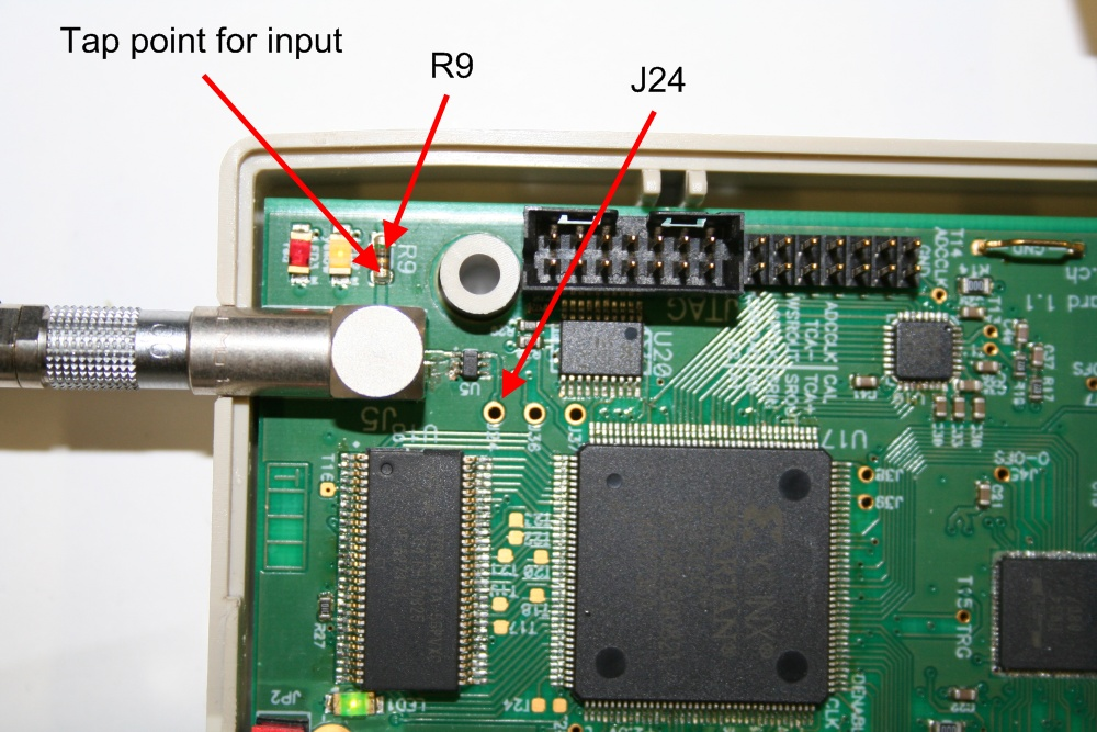
Stefan Ritt | External Trigger Input requirements | Several people mentioned that the external trigger input (TTL) does not work on the DRS4 Evaluation Board Rev. 1.1. This is not true. The requirement however is that the input signal must exceed approximately 1.8V. Since the input is terminated with 50 Ohms, not all TTL drivers may deliver enough current to exceed this threshold. To verify this, the trigger signal can be monitored with an oscilloscope at test point J24. Only if the input signal exceeds 1.8V, the signal will be seen at J24 and correctly trigger the FPGA. If the TTL driver is too weak, the termination resistor R9 can be optionally removed, but care should then be taken that reflections in the trigger input do not cause double triggers. The locations of the tap point for the input signal, the termination resistor R9 and the tap point J24 after the input level converter U5 are shown in this image:
|
|
3
|
Wed Jan 14 13:41:44 2009 |
Stefan Ritt | External Trigger Input requirements |
Another tricky issue comes from the fact that the external TTL trigger and the comparator are in a logical OR. So if the comparator level is set such that the signal is always over the threshold, the trigger is always "on" and the TTL trigger does not have any effect. It is therefore necessary to set the analog trigger level to a very high value in order to make the TTL trigger work. |
|
629
|
Wed Sep 27 16:11:03 2017 |
Yoni Sher | Event acquisition pace for irregular timing | Hi,
I'm running a LIDAR application that requires that every outgoing pulse be captured. My current setup firess sets of 20-50 pulses at 1 ms intervals, about 10 times a second, but only 10-20 pulses a second are captured.
When I fire at full speed (1KHz - one pulse every ms), about 500-600 pulses a second are captured.
At the moment, I'm triggering on channel 1 and captureing the data on channel 2. Would it help if I used the external trigger? Is there anything else I can do?
Yoni |
|
630
|
Mon Oct 2 16:08:05 2017 |
Stefan Ritt | Event acquisition pace for irregular timing | As written in the documentation, the DRS evaluaiton board has a maximum trigger capability of ~500 Hz. This is limited by the USB bus which has a finite data transfer rate. If you build your own electronics around the chip (like many other groups are doing), you can squeeze this to a few kHz, but it is some development effort.
Stefan
| Yoni Sher wrote: |
|
Hi,
I'm running a LIDAR application that requires that every outgoing pulse be captured. My current setup firess sets of 20-50 pulses at 1 ms intervals, about 10 times a second, but only 10-20 pulses a second are captured.
When I fire at full speed (1KHz - one pulse every ms), about 500-600 pulses a second are captured.
At the moment, I'm triggering on channel 1 and captureing the data on channel 2. Would it help if I used the external trigger? Is there anything else I can do?
Yoni
|
|
|
753
|
Thu Jun 20 01:36:48 2019 |
Andrew Peck | Evaluation firmware wait_vdd state | Dear Stefan,
I am working with others at UCLA on a custom made board built around the DRS4. We are in the process of writing firmware so I am adapting the readout state machine from the evaluation board firmware.
I see in the state machine of the eval board firmware that after a trigger is received, the FPGA goes into the start readout state and then into "wait_vdd", where the FPGA waits "~120 us for vdd to stabilize" before reading out the ADC.
Our application is sensitive to deadtime and this wait_vdd state adds very significantly. I am trying to find anything explaining the necessity of wait_vdd in the documentation / elog and have only found so far your old forum posting, https://elog.psi.ch/elogs/DRS4+Forum/12
Does this forum posting explain wait_vdd or is there a another purpose that I have missed?
If this post is relevant to wait_vdd, does the advice of large capacitance and an LDO with fast transient response still apply or are there any new recommendations?
Thank you,
Andrew Peck |
|
754
|
Fri Jun 21 12:54:47 2019 |
Stefan Ritt | Evaluation firmware wait_vdd state | Dear Andrew,
the posting you mention is still accurate. Any power supply will drop when you start the Domino wave, no matter how big your capacitor is. Unfortunately the output signal of the DRS4 scales with VDD. So if your VDD drops by 40 mV and you get a trigger and you immediately start the readout, the output baseline will also be shifted by about 40 mV. If you are sensitive to dead time, you can remove the wait_vdd state completely, but then you have to deal with varying baseline shifts. If you have narrow signals sitting on a broad baseline, you can correct for this by measuring the baseline outside your signal, then subtracting it before integrating your pulse. If you have lots of pile-up in your signals, it might sometimes be hard to evaluate the baseline on an event-by-event basis.
Stefan
| Andrew Peck wrote: |
|
Dear Stefan,
I am working with others at UCLA on a custom made board built around the DRS4. We are in the process of writing firmware so I am adapting the readout state machine from the evaluation board firmware.
I see in the state machine of the eval board firmware that after a trigger is received, the FPGA goes into the start readout state and then into "wait_vdd", where the FPGA waits "~120 us for vdd to stabilize" before reading out the ADC.
Our application is sensitive to deadtime and this wait_vdd state adds very significantly. I am trying to find anything explaining the necessity of wait_vdd in the documentation / elog and have only found so far your old forum posting, https://elog.psi.ch/elogs/DRS4+Forum/12
Does this forum posting explain wait_vdd or is there a another purpose that I have missed?
If this post is relevant to wait_vdd, does the advice of large capacitance and an LDO with fast transient response still apply or are there any new recommendations?
Thank you,
Andrew Peck
|
|
|
755
|
Mon Jun 24 23:07:35 2019 |
Andrew Peck | Evaluation firmware wait_vdd state | Dear Stefan,
Thanks so much for clarifying this. We made wait_vdd a parameter controlled by software and will try to experiment with it to find some compromise between deadtime and the offset added by the droop in VDD.
Best regards,
Andrew
| Stefan Ritt wrote: |
|
Dear Andrew,
the posting you mention is still accurate. Any power supply will drop when you start the Domino wave, no matter how big your capacitor is. Unfortunately the output signal of the DRS4 scales with VDD. So if your VDD drops by 40 mV and you get a trigger and you immediately start the readout, the output baseline will also be shifted by about 40 mV. If you are sensitive to dead time, you can remove the wait_vdd state completely, but then you have to deal with varying baseline shifts. If you have narrow signals sitting on a broad baseline, you can correct for this by measuring the baseline outside your signal, then subtracting it before integrating your pulse. If you have lots of pile-up in your signals, it might sometimes be hard to evaluate the baseline on an event-by-event basis.
Stefan
| Andrew Peck wrote: |
|
Dear Stefan,
I am working with others at UCLA on a custom made board built around the DRS4. We are in the process of writing firmware so I am adapting the readout state machine from the evaluation board firmware.
I see in the state machine of the eval board firmware that after a trigger is received, the FPGA goes into the start readout state and then into "wait_vdd", where the FPGA waits "~120 us for vdd to stabilize" before reading out the ADC.
Our application is sensitive to deadtime and this wait_vdd state adds very significantly. I am trying to find anything explaining the necessity of wait_vdd in the documentation / elog and have only found so far your old forum posting, https://elog.psi.ch/elogs/DRS4+Forum/12
Does this forum posting explain wait_vdd or is there a another purpose that I have missed?
If this post is relevant to wait_vdd, does the advice of large capacitance and an LDO with fast transient response still apply or are there any new recommendations?
Thank you,
Andrew Peck
|
|
|
|
153
|
Wed Feb 15 18:08:13 2012 |
Yuji Iwai | Evaluation Board v4 Trigger/Clock Connectors | Quick question - what type of connectors are used for the trigger and clock in/out on the v4 eval board? |
|
761
|
Sat Jul 13 01:00:15 2019 |
Brendan Posehn | Evaluation Board Test Functionality | Hello,
I have recently obtained a DRS4 Evaluation Board (V5), but I am unable to register signals when using the DRS Oscilloscope application. There seems to be some difference in noise when I have an input connected to a signal or not, but I am unable to view a simple, 0.2V amplitude square wave or other small signals. The only way I have been able to view a waveform is when connecting the reference clock to all channels. When running 'info' in the DRS Command Line Interface I am shown correct information. I was wondering if there is any way for me to test the functionality of the board (specifially ability to read signals on Ch 1-4) to ensure that it is indeed working as expected?
Thanks,
Brendan |
|
762
|
Mon Jul 15 17:26:50 2019 |
Stefan Ritt | Evaluation Board Test Functionality | Have you set the trigger correctly to the channel with your signal, polarity and level? Do you undersand the difference between normal and auto trigger? Why don't you post a screendump. Are you ABSOLUTELY SURE that you have a signal on your cable? Have you tried with another oscilloscope? Are you sure that your SMA connector is good?
Stefan
| Brendan Posehn wrote: |
|
Hello,
I have recently obtained a DRS4 Evaluation Board (V5), but I am unable to register signals when using the DRS Oscilloscope application. There seems to be some difference in noise when I have an input connected to a signal or not, but I am unable to view a simple, 0.2V amplitude square wave or other small signals. The only way I have been able to view a waveform is when connecting the reference clock to all channels. When running 'info' in the DRS Command Line Interface I am shown correct information. I was wondering if there is any way for me to test the functionality of the board (specifially ability to read signals on Ch 1-4) to ensure that it is indeed working as expected?
Thanks,
Brendan
|
|
|