| ID |
Date |
Author |
Subject |
|
366
|
Tue Aug 26 14:16:26 2014 |
Roman Gredig | binary files with more than 4 drs board ver. 5.0.2 | Dear Stefan
after having some problems with writing binary files with more than 4 drs boards (in multiboard-mode) I might
have found the solution.
In the file src/Osci.cpp at line 838 is:
unsigned char buffer[100000];
If I understand the binary format right, this works only with up to four boards. With the maximum number of
boards in your specification (16 boards) and all channels switched on on all boards this array needs to have
about 400000 entries (for the first event, where the time information is written too).
Could you please cross-check that?
Thank you very much!
Cheers,
Roman |
|
35
|
Mon Feb 15 19:43:34 2010 |
Ron Grazioso | Problem reading oscilloscope binary waveform output | I have saved some waveforms using the oscilloscope application in both binary and xml. I can see that the xml file gives me proper data values but when I try to read the binary file using IDL, it does not seem correct. This is a screen shot of the pulse I saved: 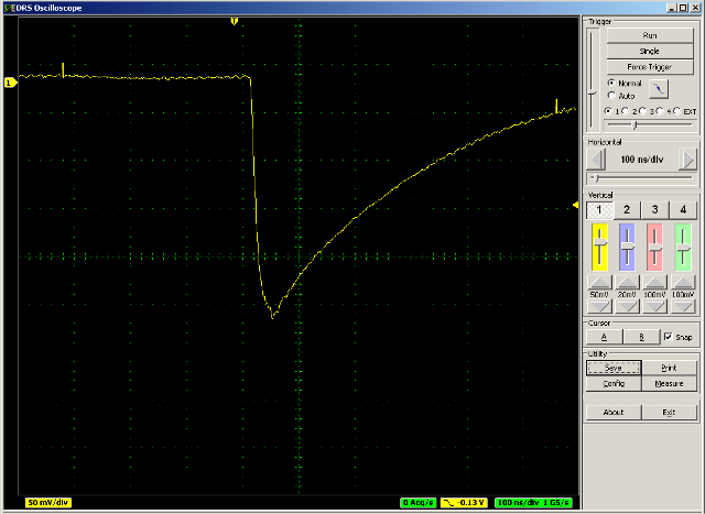
But when I open the binary file in IDL using:
data = uintarr(1024) ;unsigned integer array
readu,lun1,data
free_lun,lun1
close,lun1
;Convert bits to Volts
data=data*0.000015259-0.5
window,0,xs=512,ys=512
plot,data[*]
  I get: I get: 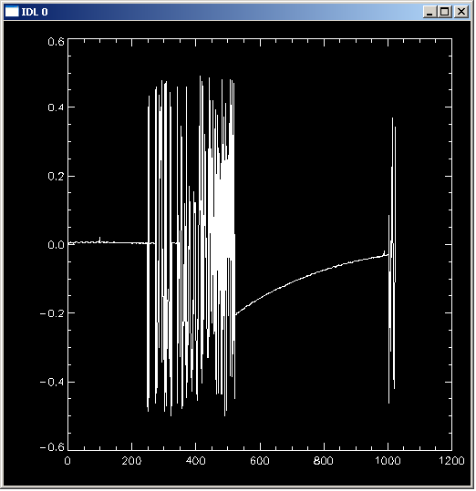
It looks like the pulse is there but there is something corrupting the data only in binary form. Is there a setting that may not be correct?
Thanks, Ron
|
|
112
|
Sat Feb 19 17:25:29 2011 |
S S Upadhya | how to synchronize Sampling frequency of two evaluation boards | Dear sir,
We have two evaluation boards of DRS4. We would like to use 8 inputs to be recorded on a trigger and we would like to find the relative time difference of inputs. So is it possible to synchronize the sampling frequency of the two evaluation boards.
with best regards
S S Upadhya |
|
115
|
Mon Feb 21 12:42:33 2011 |
S S Upadhya | how to synchronize Sampling frequency of two evaluation boards |
| Stefan Ritt wrote: |
|
| Stefan Ritt wrote: |
|
| S S Upadhya wrote: |
|
Dear sir,
We have two evaluation boards of DRS4. We would like to use 8 inputs to be recorded on a trigger and we would like to find the relative time difference of inputs. So is it possible to synchronize the sampling frequency of the two evaluation boards.
with best regards
S S Upadhya
|
No, not in this version. We plan a future version of the evaluation board with clock synchronization, but that board will not be ready before 2-3 months. Anyhow the board is more meant as an evaluation board, to test the chip and develop own electronics, and not to build a complete DAQ system. Note that CAEN distributes now a VME board containing the four DRS4 chips and 32 channels on a board.
|
Well, one thing you can do is to generate an external trigger and send it to the external trigger input of both cards. Then you can determine the time in respect to the trigger point in both boards. But since the trigger cell jitters by 2-3 cells in each chip, the accuracy is limited to about 1-2 ns when running at 2 GS/s.
|
Dear Stefan,
Thanks for the second suggestion. I wanted to do feasibility study of DRS4 application to our requirement in the experiment
Thank you again sir,
Upadhya |
|
522
|
Wed May 11 15:48:57 2016 |
SANDJONG Saturnin Orly | Probl�me de Calibration de la DRS4 | Bonjour, Je suis en stage dans un laboratoire ou on utilise pour echantillonnage des données, une cartes DRS4 5GSPS avec 1024 cell, mon probléme réside dans la partie Calibration en tension selon l'article "Novel Calibration Method for Switched Capacitor Arrays Enables Time Measurements with Sub-Picosecond Resolution".
En fait je ne comprends pas précisément ces 3 parties de la calibration en tension. Quelqu'un pourras t-il s'il vous plait m'expliquer assez clairement avec des exemples comment il faut s'y prendre?
Merci et bien Cordialement. |
|
728
|
Wed Jan 30 06:51:37 2019 |
Saurabh Neema | DRS4 domino wave stability study | We have been using DRS4 IC in our design for quite some time and it is giving good performance.
Till now we were using Domino wave frequency as 1 GSPS by use of reference clock to DRS4 and internal PLL of DRS4. Recently we tried to use 4GSPS by modifying the reference clock.
What I have found that DRS4 domino wave is more stable at 4 GSPS as compared to 1 GSPS by doing the timing jitter analysis. I am not sure if it is the property of DRS4 IC to be having more stable domino wave at higher frequency (by design) or it is due to some external effects like PLL loop filter or any other on board parasitic effects.
Please share if anyone has done any study of DRS4 Domino wave stability at different sampling frequencies.
Thanks,
|
|
302
|
Thu Nov 14 11:39:06 2013 |
Schablo | Cascading of channels | Hello, I want use cascading of channels for 2048 cell - SetChannelConfig(0,8,4), but i can't understand how . Please, help me. Where i can dowload 2048_mode.ppt. (I found information about this file in DRS.cpp (3445 line "/ combine two halfs correctly, see 2048_mode.ppt")
Best regards,
Schablo Kostya |
|
311
|
Thu Nov 21 14:35:57 2013 |
Schablo | Cascading of channels |
| Stefan Ritt wrote: |
|
| Schablo wrote: |
|
Hello, I want use cascading of channels for 2048 cell - SetChannelConfig(0,8,4), but i can't understand how . Please, help me. Where i can dowload 2048_mode.ppt. (I found information about this file in DRS.cpp (3445 line "/ combine two halfs correctly, see 2048_mode.ppt")
Best regards,
Schablo Kostya
|
You have to combine two channels into one, and depending on where the domino wave stopped, things get a bit complicated. I attach 2048_mode.ppt for your reference, but am not sure if this will really help.
/Stefan
|
Sorry for my question.
I'm trying change "drs_exam.cpp" for read 2048 cell.
I'm using SetChannnelConfig(0,8,4) and this code in "drs_exam.cpp" :
...
float arrX[2048];
float arrY[2048];
....
b->GetTime(0, b->GetTriggerCell(0), arrX);
b->GetWave(0, 0, arr.Y);
....
Return 2048 values in arrX[2048] - correct values, but in arrY[2048] - not correct values.
I can't understand what values return "GetWave" function. Please, say me how make, that GetWave function return correct values. " not - correct values "(i mean that i give signal in drs bord and values not true.)
Best regards,
Schablo Kostya
|
|
693
|
Tue May 8 23:58:35 2018 |
Sean Quinn | Manual Rev5.1 Figure 1, optional components | Dear All,
I'm troubleshooting a board which uses the DRS4 and adopts an analog front end very similar to the evaluation board. As a result, we rely on the eval board as a reference. In doing so we've encountered an issue in the manual:
The high resolution photo in Figure 1. is useful, but it seems to correspond to an older version of the board. For instance, the RF switch can't correspond to the schematics of Rev5.1 in the appendix.
Request: Could the manual be updated with a high resolution image of Rev5.1. Also, could a high resolution of the bottom side of the board be included in the manual? This is desirable since it has the version number and contact information, so it will remove any ambiguity about what board you're looking at and what schematics you should refer to.
A second question, which might be overly broad: what is the impact of installing the optional components (marked * in the schematics) on the analog front end? Why are a lot of these left uninstalled on the eval board?
Thanks,
Sean |
|
710
|
Wed Aug 1 00:49:30 2018 |
Sean Quinn | Optimal readout speed | Dear DRS4 team,
On page 3 of the data sheet, Table 1. for readout speed a typical value of 10 MHz is specified, but in the comment column it notes optimal performance achieved at 33 MHz.
I see the V5.1 eval board runs at 16 MHz. I'd like to understand the rationale for this using speed, instead of 33 MHz. Is there an SNR issue for the ADC at the higher speed, even though this is optimal for the DRS4?
Very best,
Sean |
|
722
|
Mon Nov 5 17:17:08 2018 |
Sean Quinn | Pi attenuator on eval board inputs? | Dear DRS4 team,
I am curious about this part of the circuit:
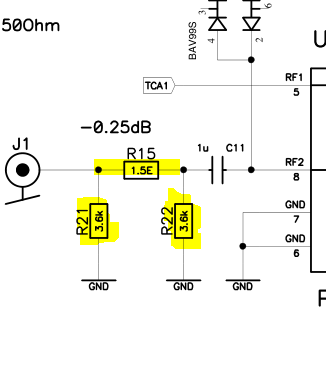
What is the purpose of this? |
|
820
|
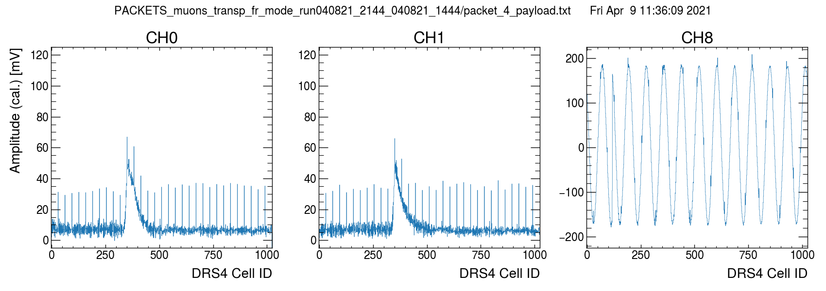
Wed Apr 7 03:29:39 2021 |
Sean Quinn | Unexpected noise in muxout: t_samp related? | Dear DRS4 team,
I'm experiencing some issues that seem to be isolated to the ASIC, and would like to understand if we are doing something wrong. There are several items to address in the post.
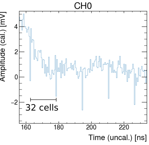
First, I do not think the noise observed is being injected from elsewhere on the board. If I run the DRS in transparent mode, the baseline noise is low, on order 3.5 mV (60 ADU), perhaps radiated from a clock. See below image. The scale is 0 to 1000 ADU with LSB = 6 uV (same AD9245 as eval board.). The DRS is in RUNNING state, I have forced a trigger in the ILA. This is for a single channel, CH0, 1024 cells.
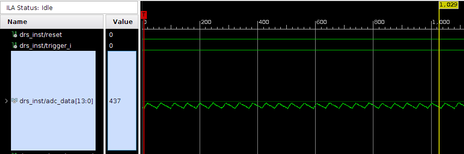
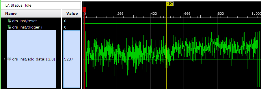
In the next image, I show the waveform obtained from a full readout. This corresponds to ADC_READOUT state, and the plot uses the same 1000 ADU scale. Noise seems around 350 ADU now, many factors worse than before.
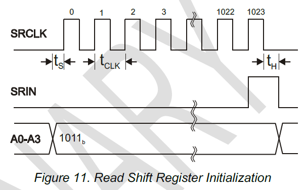
We've spent a lot of time trying to understand what's happening. One area that would be helpful to get some guidance on is the "t_samp" parameter. In Fig. 11 of the data sheet, should there be a t_samp label between t_s and t_clk? It just has arrows there with some width.
In our current firmware I believe R1 is simply one clock after R0 (for both ROI and full readout mode). Would this lead to the added noise observed in muxout?
This leads to the next question on what to actually use for t_samp. In the data sheet, page 4 "Timing Characteristics" it says to use t_samp = t0 + t_clk. Additionally, t0= 10 ns from that table. Fair enough.
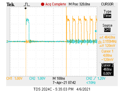
But if I check this against the eval board timing, I see very different values. Here the clock is 15 MHz so t_clk=67 ns (I note another post about this topic https://elog.psi.ch/elogs/DRS4+Forum/713), so I expect t_samp = 77 ns. But in practice it looks like the R0 to R1 delay is ~465 ns? (cyan=RSRLOAD, yellow=SRCLK)
Given this, is t_samp a value that should be tuned by the user?
Best regards,
Sean
|
|
822
|
Fri Apr 9 20:22:13 2021 |
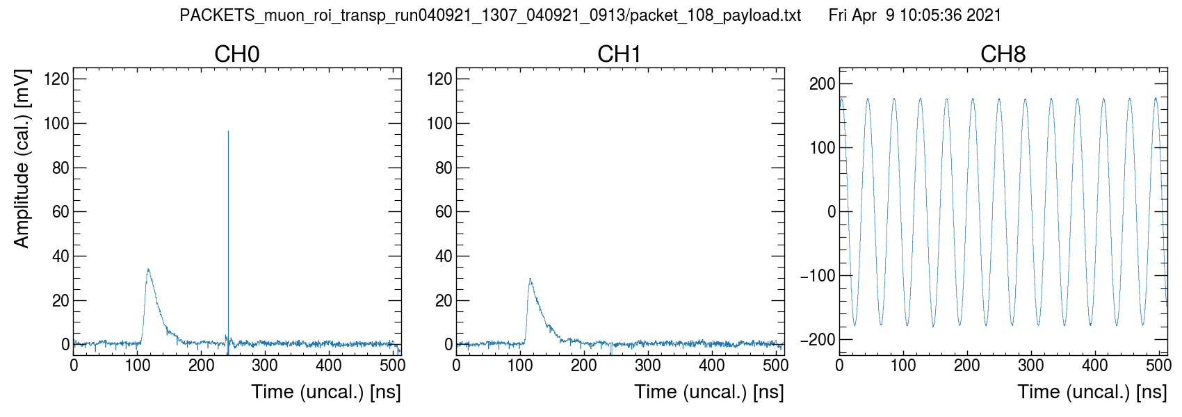
Sean Quinn | Unexpected noise in muxout: t_samp related? | Hi Stefan,
Thanks much for the quick reply. Ok, yes, things do seem ok after the offset calibration. I am running into some other issues I could use your advice on but will make a separate thread. As a preview, you can see hints in this waveform (periodic negative spikes).
This one should be considered resolved.
| Stefan Ritt wrote: |
|
Dear Sean,
noise in transparent mode comes from some coupling to your system clock. But 3.5 mV RMS seems rather hight to me. You should get it to below 1 mV if the DRS4 input is clean (try to short it).
The noise in the readout is expected. It looks exactly as Plot3 from the data sheet. You have to calibrate it away with a fixed offset for each cell as described in this paper: https://arxiv.org/abs/1405.4975 (paragraph IV. A. Voltage Calibration).
Concerning t_samp: Fig 11 in the datasheet just tells you that the rising edge of the SRCLK should come later than t_s after the address change. t_s is the setup time and 5 ns. Fig 12 tells you that the ADC should sample the analog output of the DRS t_samp after the address change A0-A3 and t_samp after the rising edge of SRCLK.
The digitizing speed of the evaluation board is indeed 15 MHz instead of the maximum 30 MHz, because this was easier to program in the FPGA. The t_samp has to be there so that the analog output signal of the DRS4 settles to its final value after each SRCLK pulse. If you sample "too early", you sample with the ADC the output when it is sill moving. So you have to wait until the analog is settled, but just before the next DRS sample becomes visible at the output. You can fine tune this with a differential probe at the DRS4 analog output (on a single ended probe you might drown in noise) on one channel of yoru scope and the ADC sample clock on the other channel of your scope. Note that the ADC sample clock cannot be derived straight from your FPGA clock, but you need some clock manager to fine-adjust its phase in 1ns steps.
But again, looking at your output, everything seems fine. You see the 5mV rms noise indicated in the datasheet table 1, which translates to about 20 mV peak-to-peak. If you do the offset calibration, this should go down to below 1 mV.
Best,
Stefan
| Sean Quinn wrote: |
|
Dear DRS4 team,
I'm experiencing some issues that seem to be isolated to the ASIC, and would like to understand if we are doing something wrong. There are several items to address in the post.
First, I do not think the noise observed is being injected from elsewhere on the board. If I run the DRS in transparent mode, the baseline noise is low, on order 3.5 mV (60 ADU), perhaps radiated from a clock. See below image. The scale is 0 to 1000 ADU with LSB = 6 uV (same AD9245 as eval board.). The DRS is in RUNNING state, I have forced a trigger in the ILA. This is for a single channel, CH0, 1024 cells.
In the next image, I show the waveform obtained from a full readout. This corresponds to ADC_READOUT state, and the plot uses the same 1000 ADU scale. Noise seems around 350 ADU now, many factors worse than before.
We've spent a lot of time trying to understand what's happening. One area that would be helpful to get some guidance on is the "t_samp" parameter. In Fig. 11 of the data sheet, should there be a t_samp label between t_s and t_clk? It just has arrows there with some width.
In our current firmware I believe R1 is simply one clock after R0 (for both ROI and full readout mode). Would this lead to the added noise observed in muxout?
This leads to the next question on what to actually use for t_samp. In the data sheet, page 4 "Timing Characteristics" it says to use t_samp = t0 + t_clk. Additionally, t0= 10 ns from that table. Fair enough.
But if I check this against the eval board timing, I see very different values. Here the clock is 15 MHz so t_clk=67 ns (I note another post about this topic https://elog.psi.ch/elogs/DRS4+Forum/713), so I expect t_samp = 77 ns. But in practice it looks like the R0 to R1 delay is ~465 ns? (cyan=RSRLOAD, yellow=SRCLK)
Given this, is t_samp a value that should be tuned by the user?
Best regards,
Sean
|
|
|
|
823
|
Fri Apr 9 20:29:45 2021 |
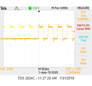
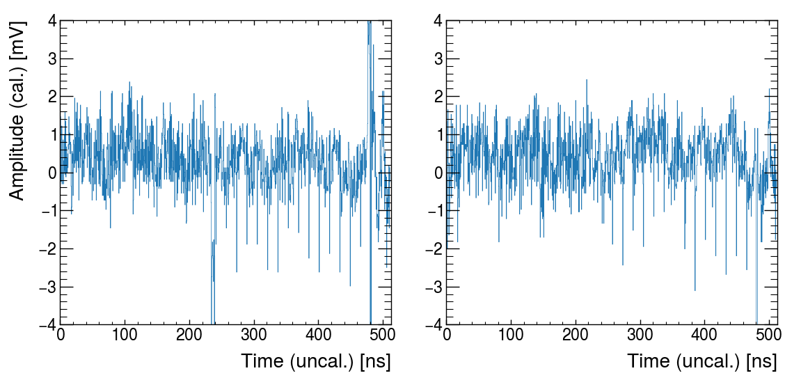
Sean Quinn | Spikes/noise sensitive to clock settings? | Dear DRS4 team,
I'm trying to troubleshoot some odd spike behavior. If I run the ADC and SR CLK at 16 MHz (behavior also seen at 33 MHz) we get very noisy data (post-calibration) with periodic spikes.
In the below plot
- CH0 & CH1 are muon pulses from a scintillator + SiPM detector
- CH8 is a 25 MHz sinewave (in phase with all generated board clocks)
- Transparent mode = ON
- ROI = OFF, "full readout mode", first sample = cell 0
- DRS REFCLK = 1 MHz (2 GS/s)
- ADC & SR CLK = 16 MHz, 0 deg. offset
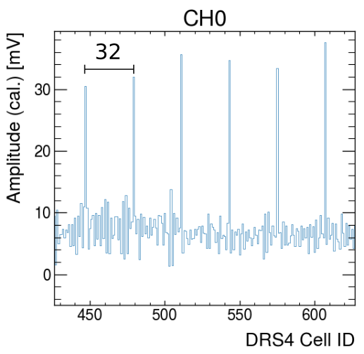
After I modify some clock settings, things seem to improve dramatically, and the spike behavior changes
- ADC and SR CLK = 15 MHz, 0 deg. offset
- Transparent mode = ON
- ROI = ON (just for testing purposes)
- Add 1.064 ns skew to DRS REF CLK
- NOTE: Unfortunately due to a design mishap, the ADC and FPGA clock use a phase-locked output pair on our clock synthesis chip, so we cannot fine-tune the skew for it.
Observed differences
- Spike polarity seems inverted
- Spikes limited to smaller number of cells now?
- Spike amplitude reduced
- Overall baseline variance seems better
- New large positive spike artifact on CH0 that seems inverted on CH1
- CH8 seems unaffected by large spikes?
Artifacts seem related to clock configuration, but I am sort of in the dark on what might be happening from a first-principles point of view. Any tips?
Warm regards,
Sean |
|
826
|
Fri Apr 9 21:56:54 2021 |
Sean Quinn | Unexpected noise in muxout: t_samp related? | Yes, there is some systematic board noise on this prototype, unfortunately 
Ok, then it seems the other post I made might still belong in this thread after all.
Thanks for confirming negative spike behavior, we now have a mitigation plan going forward.
Cheers,
| Stefan Ritt wrote: |
|
If you do the cell calibration correctly, your noise should be ~0.4 mV. You seem to be 2-3x larger. The periodic negative spikes come if you dont' sample at the right time. Adjust t_samp until they are gone.
Stefan
| Sean Quinn wrote: |
|
Hi Stefan,
Thanks much for the quick reply. Ok, yes, things do seem ok after the offset calibration. I am running into some other issues I could use your advice on but will make a separate thread. As a preview, you can see hints in this waveform (periodic negative spikes).
This one should be considered resolved.
| Stefan Ritt wrote: |
|
Dear Sean,
noise in transparent mode comes from some coupling to your system clock. But 3.5 mV RMS seems rather hight to me. You should get it to below 1 mV if the DRS4 input is clean (try to short it).
The noise in the readout is expected. It looks exactly as Plot3 from the data sheet. You have to calibrate it away with a fixed offset for each cell as described in this paper: https://arxiv.org/abs/1405.4975 (paragraph IV. A. Voltage Calibration).
Concerning t_samp: Fig 11 in the datasheet just tells you that the rising edge of the SRCLK should come later than t_s after the address change. t_s is the setup time and 5 ns. Fig 12 tells you that the ADC should sample the analog output of the DRS t_samp after the address change A0-A3 and t_samp after the rising edge of SRCLK.
The digitizing speed of the evaluation board is indeed 15 MHz instead of the maximum 30 MHz, because this was easier to program in the FPGA. The t_samp has to be there so that the analog output signal of the DRS4 settles to its final value after each SRCLK pulse. If you sample "too early", you sample with the ADC the output when it is sill moving. So you have to wait until the analog is settled, but just before the next DRS sample becomes visible at the output. You can fine tune this with a differential probe at the DRS4 analog output (on a single ended probe you might drown in noise) on one channel of yoru scope and the ADC sample clock on the other channel of your scope. Note that the ADC sample clock cannot be derived straight from your FPGA clock, but you need some clock manager to fine-adjust its phase in 1ns steps.
But again, looking at your output, everything seems fine. You see the 5mV rms noise indicated in the datasheet table 1, which translates to about 20 mV peak-to-peak. If you do the offset calibration, this should go down to below 1 mV.
Best,
Stefan
| Sean Quinn wrote: |
|
Dear DRS4 team,
I'm experiencing some issues that seem to be isolated to the ASIC, and would like to understand if we are doing something wrong. There are several items to address in the post.
First, I do not think the noise observed is being injected from elsewhere on the board. If I run the DRS in transparent mode, the baseline noise is low, on order 3.5 mV (60 ADU), perhaps radiated from a clock. See below image. The scale is 0 to 1000 ADU with LSB = 6 uV (same AD9245 as eval board.). The DRS is in RUNNING state, I have forced a trigger in the ILA. This is for a single channel, CH0, 1024 cells.
In the next image, I show the waveform obtained from a full readout. This corresponds to ADC_READOUT state, and the plot uses the same 1000 ADU scale. Noise seems around 350 ADU now, many factors worse than before.
We've spent a lot of time trying to understand what's happening. One area that would be helpful to get some guidance on is the "t_samp" parameter. In Fig. 11 of the data sheet, should there be a t_samp label between t_s and t_clk? It just has arrows there with some width.
In our current firmware I believe R1 is simply one clock after R0 (for both ROI and full readout mode). Would this lead to the added noise observed in muxout?
This leads to the next question on what to actually use for t_samp. In the data sheet, page 4 "Timing Characteristics" it says to use t_samp = t0 + t_clk. Additionally, t0= 10 ns from that table. Fair enough.
But if I check this against the eval board timing, I see very different values. Here the clock is 15 MHz so t_clk=67 ns (I note another post about this topic https://elog.psi.ch/elogs/DRS4+Forum/713), so I expect t_samp = 77 ns. But in practice it looks like the R0 to R1 delay is ~465 ns? (cyan=RSRLOAD, yellow=SRCLK)
Given this, is t_samp a value that should be tuned by the user?
Best regards,
Sean
|
|
|
|
|
|
894
|
Mon Oct 17 16:29:37 2022 |
Sebastian Infante | DRS4 installation via tar in ubuntu not working | Hello i cant install any the last versions that i downloaded from the dropbox, i can untar the file called drs-5.0.6 and when i type "make" while inside the extracted folder that starts working properly till a point and i get an error, its worth mention that i installed wxWidgets and could make a simple hello world that worked properly in wxWidgets.
The error that i get is the next one:
inlined from ‘bool ResponseCalibration::ReadCalibrationV4(unsigned int)’ at src/DRS.cpp:7224:35:
/usr/include/x86_64-linux-gnu/bits/string_fortified.h:95:34: warning: ‘char* __builtin___strncpy_chk(char*, const char*, long unsigned int, long unsigned int)’ specified bound depends on the length of the source argument [-Wstringop-truncation]
95 | return __builtin___strncpy_chk (__dest, __src, __len,
| ~~~~~~~~~~~~~~~~~~~~~~~~^~~~~~~~~~~~~~~~~~~~~~
96 | __glibc_objsize (__dest));
| ~~~~~~~~~~~~~~~~~~~~~~~~~
src/DRS.cpp: In member function ‘bool ResponseCalibration::ReadCalibrationV4(unsigned int)’:
src/DRS.cpp:4767:11: note: length computed here
4767 | strncpy(calibrationDirectoryPath, fCalibDirectory, strlen(fCalibDirectory));
| ~~~~~~~^~~~~~~~~~~~~~~~~~~~~~~~~~~~~~~~~~~~~~~~~~~~~~~~~~~~~~~~~~~~~~~~~~~~
In file included from /usr/include/string.h:535,
from /usr/local/include/wx-3.3/wx/string.h:30,
from /usr/local/include/wx-3.3/wx/memory.h:15,
from /usr/local/include/wx-3.3/wx/object.h:19,
from /usr/local/include/wx-3.3/wx/wx.h:15,
from src/DRS.cpp:15:
In function ‘char* strncpy(char*, const char*, size_t)’,
inlined from ‘void DRSBoard::GetCalibrationDirectory(char*)’ at src/DRS.cpp:4767:11,
inlined from ‘bool ResponseCalibration::ReadCalibrationV3(unsigned int)’ at src/DRS.cpp:7066:35:
/usr/include/x86_64-linux-gnu/bits/string_fortified.h:95:34: warning: ‘char* __builtin___strncpy_chk(char*, const char*, long unsigned int, long unsigned int)’ specified bound depends on the length of the source argument [-Wstringop-truncation]
95 | return __builtin___strncpy_chk (__dest, __src, __len,
| ~~~~~~~~~~~~~~~~~~~~~~~~^~~~~~~~~~~~~~~~~~~~~~
96 | __glibc_objsize (__dest));
| ~~~~~~~~~~~~~~~~~~~~~~~~~
src/DRS.cpp: In member function ‘bool ResponseCalibration::ReadCalibrationV3(unsigned int)’:
src/DRS.cpp:4767:11: note: length computed here
4767 | strncpy(calibrationDirectoryPath, fCalibDirectory, strlen(fCalibDirectory));
| ~~~~~~~^~~~~~~~~~~~~~~~~~~~~~~~~~~~~~~~~~~~~~~~~~~~~~~~~~~~~~~~~~~~~~~~~~~~
g++ -g -O2 -Wall -Wuninitialized -fno-strict-aliasing -Iinclude -I/usr/local/include -DOS_LINUX -DHAVE_USB -DHAVE_LIBUSB10 -DUSE_DRS_MUTEX -I/usr/local/lib/wx/include/gtk3-unicode-3.3 -I/usr/local/include/wx-3.3 -D_FILE_OFFSET_BITS=64 -DWXUSINGDLL -D__WXGTK__ -pthread -c src/averager.cpp
g++ -g -O2 -Wall -Wuninitialized -fno-strict-aliasing -Iinclude -I/usr/local/include -DOS_LINUX -DHAVE_USB -DHAVE_LIBUSB10 -DUSE_DRS_MUTEX -I/usr/local/lib/wx/include/gtk3-unicode-3.3 -I/usr/local/include/wx-3.3 -D_FILE_OFFSET_BITS=64 -DWXUSINGDLL -D__WXGTK__ -pthread -c src/ConfigDialog.cpp
In file included from include/DRSOscInc.h:25,
from src/ConfigDialog.cpp:7:
include/DOFrame.h: In member function ‘bool DOFrame::GetRefclk()’:
include/DOFrame.h:111:46: error: ordered comparison of pointer with integer zero (‘bool*’ and ‘int’)
111 | bool GetRefclk() { return m_refClk > 0; }
| ~~~~~~~~~^~~
make: *** [Makefile:81: ConfigDialog.o] Error 1
|
|
800
|
Wed Oct 21 15:03:13 2020 |
Seiya Nozaki | Timing diagram of SROUT/SRIN signal to write/read a write shift register | Dear Stefan,
I have questions about the timing diagram of SROUT/SRIN signal to write/read a write shift register.
1) Value of SRIN signal is saved at the falling edge of SRCLK, correct? (It is written in datasheet, page12, "Bits are latched into the shift register on the falling edge of SRCLK")
2) When are 8-bits of write shift register shown through SROUT? At ridging edges of SRCLK? and with additional delay(~10ns)? or falling edges?
3) In my understanding, when SRCLK is sent to DRS4, we can read and write the values in parallel, right? If so, is it possible just to read the registers without updating the registers?
[Background]
We have two modes to set the write shift register, the first one is to always reconnect to the first line and another one is to reconnect to the same line as when DWRITE goes to Low.
We can read/write the write shift register with the first mode (channel reset, page1). But we rarely face the problem of write shift register, unexpected values are written, with the second mode. With this mode, SROUT signal is sent back to DRS from FPGA as SRIN to write the same value on the write shift register. So there is a small delay(~10ns) due to the routing (DRS->FPGA->DRS, page2). It seems SRIN signal is not stable around the falling edges of SRCLK, thus it could cause that unexpected values are written in write shifter register.
To understand the situation clearly, I'd like to know the answer to the above questions.
Thank you.
Best regards,
Seiya |
|
802
|
Tue Oct 27 15:02:09 2020 |
Seiya Nozaki | Timing diagram of SROUT/SRIN signal to write/read a write shift register | Dear Stefan,
Thank you for your reply.
SRIN is directly connected to SROUT via FPGA for now, but it is unstable for the timing between clock and SRIN depending on the firmware logic.
We want to make our system more robust, so we are thinking to use a clock with a lower frequency (let's say 16.6 MHz) or change the duty cycle of a clock to keep more time between the rising edge and falling edge of a clock. This change is just for reading/writing the write shift register, we will use a 33 MHz clock for the analog readout in any case.
If we change like above, are there any concerns from the DRS4 side?
Best,
Seiya
| Stefan Ritt wrote: |
|
Dear Seiya,
1) That's correct. SRIN is ampled at the falling edge. Pleae make sure to obey the hold-time as written in the datasheet. P.12, Fig. 11: SRIN must be stable before the falling edge of SRCLK and tH after the falling clock. tH is 5ns according to table 1.
2) The write shift register is a 8-bit shift register, with an input, output and clock. After the first clock pulse, the 7th bit is shown, after the second clock pulse the 6th bit and so on. You you need 8 clock pulses to read the whole register. At the same time you write to the register, so what ever is present at SRIN will replace the old 8 bits of that register.
3) No this is not possible. When you read the register, you write to it at the same time. One possibilty is to connect SROUT to SRIN during that (maybe via the FPGA). Then you have a circular register wich is the same after each 8 clock pulses.
For your reference, I posted a commercial D-Flip Flop (TI SNHCS72). The DRS4 write shift register is a simple array of 8 such registers, with no CLR or PRE, where SROUT is Q of the last Flip Flop.
Best,
Stefan
| Seiya Nozaki wrote: |
|
Dear Stefan,
I have questions about the timing diagram of SROUT/SRIN signal to write/read a write shift register.
1) Value of SRIN signal is saved at the falling edge of SRCLK, correct? (It is written in datasheet, page12, "Bits are latched into the shift register on the falling edge of SRCLK")
2) When are 8-bits of write shift register shown through SROUT? At ridging edges of SRCLK? and with additional delay(~10ns)? or falling edges?
3) In my understanding, when SRCLK is sent to DRS4, we can read and write the values in parallel, right? If so, is it possible just to read the registers without updating the registers?
[Background]
We have two modes to set the write shift register, the first one is to always reconnect to the first line and another one is to reconnect to the same line as when DWRITE goes to Low.
We can read/write the write shift register with the first mode (channel reset, page1). But we rarely face the problem of write shift register, unexpected values are written, with the second mode. With this mode, SROUT signal is sent back to DRS from FPGA as SRIN to write the same value on the write shift register. So there is a small delay(~10ns) due to the routing (DRS->FPGA->DRS, page2). It seems SRIN signal is not stable around the falling edges of SRCLK, thus it could cause that unexpected values are written in write shifter register.
To understand the situation clearly, I'd like to know the answer to the above questions.
Thank you.
Best regards,
Seiya
|
|
|
|
804
|
Wed Oct 28 04:32:19 2020 |
Seiya Nozaki | Timing diagram of SROUT/SRIN signal to write/read a write shift register | Dear Stefan,
OK, it's good to hear! Thank you!
Best,
Seiya
| Stefan Ritt wrote: |
|
This is a static shift register, so you can make the clock as slow as you want. Actually I don't use a "clock", I just use a data pin I control via a state machine in the VHDL code. This way I have more control over the edges. I need several (internal) clock cycles to produce one SRCLK clock cycle, but that does not matter for the DRS.
Stefan
| Seiya Nozaki wrote: |
|
Dear Stefan,
Thank you for your reply.
SRIN is directly connected to SROUT via FPGA for now, but it is unstable for the timing between clock and SRIN depending on the firmware logic.
We want to make our system more robust, so we are thinking to use a clock with a lower frequency (let's say 16.6 MHz) or change the duty cycle of a clock to keep more time between the rising edge and falling edge of a clock. This change is just for reading/writing the write shift register, we will use a 33 MHz clock for the analog readout in any case.
If we change like above, are there any concerns from the DRS4 side?
Best,
Seiya
| Stefan Ritt wrote: |
|
Dear Seiya,
1) That's correct. SRIN is ampled at the falling edge. Pleae make sure to obey the hold-time as written in the datasheet. P.12, Fig. 11: SRIN must be stable before the falling edge of SRCLK and tH after the falling clock. tH is 5ns according to table 1.
2) The write shift register is a 8-bit shift register, with an input, output and clock. After the first clock pulse, the 7th bit is shown, after the second clock pulse the 6th bit and so on. You you need 8 clock pulses to read the whole register. At the same time you write to the register, so what ever is present at SRIN will replace the old 8 bits of that register.
3) No this is not possible. When you read the register, you write to it at the same time. One possibilty is to connect SROUT to SRIN during that (maybe via the FPGA). Then you have a circular register wich is the same after each 8 clock pulses.
For your reference, I posted a commercial D-Flip Flop (TI SNHCS72). The DRS4 write shift register is a simple array of 8 such registers, with no CLR or PRE, where SROUT is Q of the last Flip Flop.
Best,
Stefan
| Seiya Nozaki wrote: |
|
Dear Stefan,
I have questions about the timing diagram of SROUT/SRIN signal to write/read a write shift register.
1) Value of SRIN signal is saved at the falling edge of SRCLK, correct? (It is written in datasheet, page12, "Bits are latched into the shift register on the falling edge of SRCLK")
2) When are 8-bits of write shift register shown through SROUT? At ridging edges of SRCLK? and with additional delay(~10ns)? or falling edges?
3) In my understanding, when SRCLK is sent to DRS4, we can read and write the values in parallel, right? If so, is it possible just to read the registers without updating the registers?
[Background]
We have two modes to set the write shift register, the first one is to always reconnect to the first line and another one is to reconnect to the same line as when DWRITE goes to Low.
We can read/write the write shift register with the first mode (channel reset, page1). But we rarely face the problem of write shift register, unexpected values are written, with the second mode. With this mode, SROUT signal is sent back to DRS from FPGA as SRIN to write the same value on the write shift register. So there is a small delay(~10ns) due to the routing (DRS->FPGA->DRS, page2). It seems SRIN signal is not stable around the falling edges of SRCLK, thus it could cause that unexpected values are written in write shifter register.
To understand the situation clearly, I'd like to know the answer to the above questions.
Thank you.
Best regards,
Seiya
|
|
|
|
|
|
756
|
Tue Jun 25 23:04:29 2019 |
Si Xie | drs_exam is always reading out a sin wave | We are using the drs_exam.cpp to read out waveforms, but it seems to be outputting only sin waves on all channels - as if it was reading out the simulated waveform from the oscilloscope program if we run it without the board plugged in. Does anyone know what is causing this?
We are taking data with a pulser plugged into channel 1, which produces a single pulse with width of 8ns, and nothing plugged into channel 2.
Our board is as follows:
Found DRS4 evaluation board, serial #2567, firmware revision 21305
Board type: 9
The output is something like the following:
Event #0 ----------------------
t1[ns] u1[mV] t2[ns] u2[mV]
0.000 -452.7 0.026 -469.3
0.289 -460.8 0.293 -469.8
0.413 -477.3 0.400 -481.5
0.642 -485.3 0.650 -482.4
0.806 -486.9 0.821 -477.8
1.086 -476.8 1.085 -457.2
1.183 -467.3 1.162 -446.4
1.450 -435.6 1.459 -405.1
1.619 -410.1 1.630 -373.3
1.843 -366.2 1.851 -323.9
1.945 -342.9 1.948 -298.9
2.221 -275.7 2.210 -229.3
2.359 -237.6 2.357 -187.6
2.602 -165.6 2.609 -111.2
2.687 -141.1 2.697 -84.3
2.976 -50.5 2.987 5.5
3.164 8.4 3.144 53.3
3.377 73.9 3.384 124.2
3.503 111.4 3.506 158.0
3.753 182.0 3.769 226.9
3.924 227.5 3.929 265.8
|
|