ID |
Date |
Author |
Subject |
|
1
|
Mon Dec 15 13:37:38 2008 |
Stefan Ritt | Welcome | Welcome to the DRS4 Discussion Forum. This forum contains information and discussions related to the DRS4 chip. Please subscribe to this forum to receive automatic email updates. If you have any technical questions, please feel free to post it here. |
|
2
|
Wed Jan 14 12:02:04 2009 |
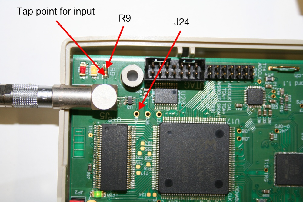
Stefan Ritt | External Trigger Input requirements | Several people mentioned that the external trigger input (TTL) does not work on the DRS4 Evaluation Board Rev. 1.1. This is not true. The requirement however is that the input signal must exceed approximately 1.8V. Since the input is terminated with 50 Ohms, not all TTL drivers may deliver enough current to exceed this threshold. To verify this, the trigger signal can be monitored with an oscilloscope at test point J24. Only if the input signal exceeds 1.8V, the signal will be seen at J24 and correctly trigger the FPGA. If the TTL driver is too weak, the termination resistor R9 can be optionally removed, but care should then be taken that reflections in the trigger input do not cause double triggers. The locations of the tap point for the input signal, the termination resistor R9 and the tap point J24 after the input level converter U5 are shown in this image:
|
|
3
|
Wed Jan 14 13:41:44 2009 |
Stefan Ritt | External Trigger Input requirements |
Another tricky issue comes from the fact that the external TTL trigger and the comparator are in a logical OR. So if the comparator level is set such that the signal is always over the threshold, the trigger is always "on" and the TTL trigger does not have any effect. It is therefore necessary to set the analog trigger level to a very high value in order to make the TTL trigger work. |
|
4
|
Wed Feb 11 12:21:07 2009 |
Stefan Ritt | Corrected datasheet Rev. 0.8 | Please note the new datasheet Rev. 0.8 available from the DRS web site. It fixes the label of pin #76, which was AGND but is actualy AVDD. The input IN8+ is located at pin #20 and not at pin #19 as described in the old table 2. |
|
5
|
Mon Feb 23 09:24:24 2009 |
Stefan Ritt | Rise-time measurements | Many applications using the DRS4 need to measure fast rising signals, like for PMTs or MCPs. This short note shows the minimal rise-times which can be measured with different input signal conditioning.
Evaluation Board
The evaluation board contains four passive transformers ADT1-1WT from Mini-Circuits to convert the single-ended input signal into a differential signal. Although these parts are rated 800 MHz bandwidth (-3dB), they have hard time to drive the DRS4 inputs. This is because at high frequencies the input impedance of DRS4 becomes pretty small (~20 Ohm at 500 MHz) due to its capacitive nature. Furthermore, each transformer drives two DRS4 inputs (channel cascading) which enhances this problem by a factor of two. We made a quick test sending a signal to the evaluation board with a rise time of 277ps and a fall time of 280ps. The result measured with the evaluation board is seen here:
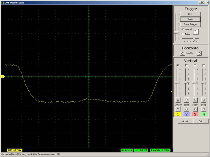
The measured rise-time (10%-90%) is only about 2ns. Disconnecting the second channel from each transformer improves this situation a bit:
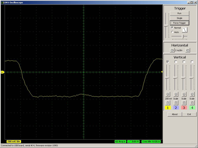
so the rise-time comes down to ~1.6ns.
Active ADA4937 driver
We tested the behavior using an active buffer ADA4937 to replace the passive transformer. Without the DRS4 connected to this buffer, we measured with the oscilloscope a rise time of 408ps and a fall time of 644ps. When we connect the DRS4 (single channel), this values increase to 702ps (rise) and 1400ps (fall), all measured with a differential oscilloscope probe (WL300 4 GHz Bandwidth, LeCroy 7300A, 3 GHz Bandwidth). In this case the rise time seen by the DRS4 is wieth ~700ps accordingly shorter:
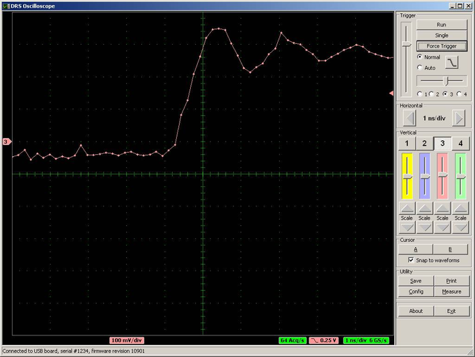
(The signal was not properly terminated and therefore we have a small overswing).
Conclusion
To obtain an optimal rise-time measurement, the design of the input stage is rather important. A fast active driver seems to do a better job than a passive transformer (which was used on the evaluation board for power reasons). Connecting only one DRS4 channel to the input improves the rise-time measurement significantly. If channel cascading is still needed, a design should use one driver for each channel, and not driver two or more DRS4 inputs from a single buffer.
If anybody comes up with an even better input driver, I'm happy to publish the results here. |
|
6
|
Mon Apr 27 15:09:49 2009 |
Stefan Ritt | Amplitude and Timing calibration for DRS4 Evaluation Board | This is a quick notification to all users of the current DRS4 evaluation board.
As you all know, the DRS4 chip needs some calibration for each individual cell which corrects the offset and the non-equidistant width in time. While the first evaluation boards have been shipped without this calibration, the current version of the software implements a full amplitude and timing calibration. The offset correction reduces the noise of the board by almost an order of magnitude to below 1 mV RMS. The timing calibration using an on-board reference clock allows a timing accuracy in the order of 10 ps. To illustrate that the following two pictures show a reference clock signal before and after timing calibration:
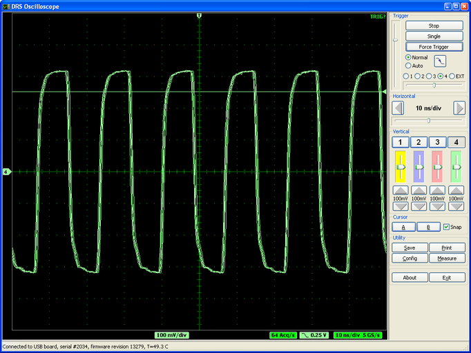
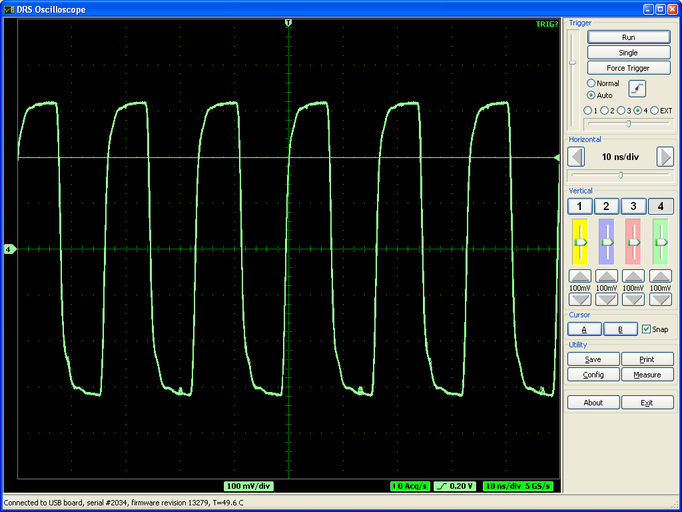
The integral temporal nonlineairy at 5 GSPS before timing calibration is about 600 ps as can be seen by the jitter of the overlaid waveforms.
In order to do a timing calibration, the firmware revison 13297 or later is required. The current software package 2.1 contains an updated firmware, but unfortunately one needs a Xilinx download cable to flash this new firmware (see http://drs.web.psi.ch/download/ under "Software Versions"). If some people want an update but do not want to buy such a cable, we offer a free update at our institute (just the postage has to be paid). The old evaluation board (Rev. 1.0, plastic housing) can unfortunately not be updated.
After the offset calibration is made, there are small (~20mV) short spikes left. They probably come from some cross-talk between the USB interface and the analog part of the board. This is currently under investigation. If new updates become available, they will be announced in this forum.
April 27th, 2009,
Stefan Ritt |
|
7
|
Tue Apr 28 11:44:07 2009 |
Stefan Ritt | Simple example application to read a DRS evaluation board | Several people asked for s simple application to guide them in writing their own application to read out a DRS board. Such an application has been added in software revions 2.1.1 and is attached to this message. This example program drs_exam.cpp written in C++ does the following necessary steps to access a DRS board:
- Crate a "DRS" object and scan all USB devices
- Display found DRS boards
- Initialize the first found board and set the sampling frequency to 5 GSPS
- Enable internal trigger on channel #1 with 250 mV threshold
- Start acquisition and wait for a trigger
- Read two waveforms (both time and amplitude)
- Repeat this 10 times
I know that we are still missing a good documentation for the DRS API, but I have not yet found the time to do that. I hope the example program is enough for most people to start writing own programs. For Windows users (MS Visual C++ 8.0) there is a drs.sln project file, and for linux users there is a Makefile which can be used to compile this example program.
|
| Attachment 1: drs_exam.cpp
|
/********************************************************************\

  Name:         drs_exam.cpp
  Created by:   Stefan Ritt

  Contents:     Simple example application to read out a DRS4
                evaluation board

  $Id: drs_exam.cpp 13344 2009-04-28 07:34:45Z ritt@PSI.CH $

\********************************************************************/

#include <math.h>

#ifdef _MSC_VER

#include <windows.h>

#elif defined(OS_LINUX)

#define O_BINARY 0

#include <unistd.h>
#include <ctype.h>
#include <sys/ioctl.h>
#include <errno.h>

#define DIR_SEPARATOR '/'

#endif

#include <stdio.h>
#include <string.h>
#include <stdlib.h>

#include "strlcpy.h"
#include "DRS.h"

/*------------------------------------------------------------------*/

int main()
{
   int i, j, nBoards;
   DRS *drs;
   DRSBoard *b;
   float time_array[1024];
   float wave_array[8][1024];

   /* do initial scan */
   drs = new DRS();

   /* show any found board(s) */
   for (i=0 ; i<drs->GetNumberOfBoards() ; i++) {
      b = drs->GetBoard(i);
      printf("Found DRS4 evaluation board, serial #%d, firmware revision %d\n",
         b->GetBoardSerialNumber(), b->GetFirmwareVersion());
   }

   /* exit if no board found */
   nBoards = drs->GetNumberOfBoards();
   if (nBoards == 0) {
      printf("No DRS4 evaluation board found\n");
      return 0;
   }

   /* continue working with first board only */
   b = drs->GetBoard(0);

   /* initialize board */
   b->Init();

   /* set sampling frequency */
   b->SetFrequency(5);

   /* enable transparent mode needed for analog trigger */
   b->SetTranspMode(1);

   /* use following line to disable hardware trigger */
   //b->EnableTrigger(0, 0);

   /* use following line to enable external hardware trigger (Lemo) */
   //b->EnableTrigger(1, 0);

   /* use following lines to enable hardware trigger on CH1 at 250 mV positive edge */
   b->EnableTrigger(0, 1);              // lemo off, analog trigger on
   b->SetTriggerSource(0);              // use CH1 as source
   b->SetTriggerLevel(0.25, false, 0);  // 0.25 V, positive edge, zero delay

   /* repeat ten times */
   for (j=0 ; j<10 ; j++) {

      /* start board (activate domino wave) */
      b->StartDomino();

      /* wait for trigger */
      printf("Waiting for trigger...");
      while (b->IsBusy());

      /* read all waveforms */
      b->TransferWaves(0, 8);

      /* read time (X) array in ns */
      b->GetTime(0, time_array);

      /* decode waveform (Y) array first channel in mV */
      b->GetWave(0, 0, wave_array[0]);

      /* decode waveform (Y) array second channel in mV*/
      b->GetWave(0, 1, wave_array[1]);

      /* process waveform: add here some code to display or save waveform X=time[i], Y=wave_array[n][i] */

      /* print some progress indication */
      printf("\rEvent #%d read successfully\n", j);
   }

   /* delete DRS object -> close USB connection */
   delete drs;
}
|
|
8
|
Wed Apr 29 07:57:33 2009 |
Stefan Ritt | Simple example application to read a DRS evaluation board |
| Stefan Ritt wrote: |
|
Several people asked for s simple application to guide them in writing their own application to read out a DRS board. Such an application has been added in software revions 2.1.1 and is attached to this message. This example program drs_exam.cpp written in C++ does the following necessary steps to access a DRS board:
- Crate a "DRS" object and scan all USB devices
- Display found DRS boards
- Initialize the first found board and set the sampling frequency to 5 GSPS
- Enable internal trigger on channel #1 with 250 mV threshold
- Start acquisition and wait for a trigger
- Read two waveforms (both time and amplitude)
- Repeat this 10 times
I know that we are still missing a good documentation for the DRS API, but I have not yet found the time to do that. I hope the example program is enough for most people to start writing own programs. For Windows users (MS Visual C++ 8.0) there is a drs.sln project file, and for linux users there is a Makefile which can be used to compile this example program.
|
One note: The program drs_exam.cpp published in the previous message needs the current version of the DRS library in DRS.cpp and DRS.h. They are contained in the software release 2.1.1 which has to be downloaded. For simplicity, I attached the two files to this message. |
| Attachment 1: DRS.cpp
|
/********************************************************************

  Name:         DRS.cpp
  Created by:   Stefan Ritt, Matthias Schneebeli

  Contents:     Library functions for DRS mezzanine and USB boards

  $Id: DRS.cpp 13351 2009-04-28 11:12:54Z ritt@PSI.CH $

\********************************************************************/

#include <stdio.h>
#include <math.h>
#include <string.h>
#include <stdlib.h>
#include <time.h>
#include <assert.h>
#include <algorithm>
#include <sys/stat.h>
#include "strlcpy.h"

#ifdef _MSC_VER
#pragma warning(disable:4996)
#   include <windows.h>
#   include <direct.h>
#else
#   include <unistd.h>
#   include <sys/time.h>
inline void Sleep(useconds_t x)
{
   usleep(x * 1000);
}
#endif

#ifdef _MSC_VER
#include <conio.h>
#define drs_kbhit() kbhit()
#else
#include <sys/ioctl.h>
int drs_kbhit()
{
   int n;

   ioctl(0, FIONREAD, &n);
   return (n > 0);
}
static inline int getch()
{
   return getchar();
}
#endif

#include <DRS.h>

#ifdef _MSC_VER
extern "C" {
#endif

#include <mxml.h>

#ifdef _MSC_VER
}
#endif

/*---- minimal FPGA firmvare version required for this library -----*/
const int REQUIRED_FIRMWARE_VERSION_DRS2 = 5268;
const int REQUIRED_FIRMWARE_VERSION_DRS3 = 6981;
const int REQUIRED_FIRMWARE_VERSION_DRS4 = 13191;

/*---- VME addresses -----------------------------------------------*/
#ifdef HAVE_VME
/* assuming following DIP Switch settings:

   SW1-1: 1 (off)       use geographical addressing (1=left, 21=right)
   SW1-2: 1 (off)       \
   SW1-3: 1 (off)        >  VME_WINSIZE = 8MB, subwindow = 1MB
   SW1-4: 0 (on)        /
   SW1-5: 0 (on)        reserverd
   SW1-6: 0 (on)        reserverd
   SW1-7: 0 (on)        reserverd
   SW1-8: 0 (on)       \
                        |
   SW2-1: 0 (on)        |
   SW2-2: 0 (on)        |
   SW2-3: 0 (on)        |
   SW2-4: 0 (on)        > VME_ADDR_OFFSET = 0
   SW2-5: 0 (on)        |
   SW2-6: 0 (on)        |
   SW2-7: 0 (on)        |
   SW2-8: 0 (on)       /

   which gives
     VME base address = SlotNo * VME_WINSIZE + VME_ADDR_OFFSET
                      = SlotNo * 0x80'0000
*/
#define GEVPC_BASE_ADDR           0x00000000
#define GEVPC_WINSIZE               0x800000
#define GEVPC_USER_FPGA   (GEVPC_WINSIZE*2/8)
#define PMC1_OFFSET                  0x00000
#define PMC2_OFFSET                  0x80000
#define PMC_CTRL_OFFSET              0x00000    /* all registers 32 bit */
#define PMC_STATUS_OFFSET            0x10000
#define PMC_FIFO_OFFSET              0x20000
#define PMC_RAM_OFFSET               0x40000
#endif                          // HAVE_VME
/*---- USB addresses -----------------------------------------------*/
#define USB_TIMEOUT                     1000    // one second
#ifdef HAVE_USB
#define USB_CTRL_OFFSET                 0x00    /* all registers 32 bit */
#define USB_STATUS_OFFSET               0x40
#define USB_RAM_OFFSET                  0x80
#define USB_CMD_IDENT                      0    // Query identification
#define USB_CMD_ADDR                       1    // Address cycle
#define USB_CMD_READ                       2    // "VME" read <addr><size>
#define USB_CMD_WRITE                      3    // "VME" write <addr><size>
#define USB_CMD_READ12                     4    // 12-bit read <LSB><MSB>
#define USB_CMD_WRITE12                    5    // 12-bit write <LSB><MSB>

#define USB2_CMD_READ                      1
#define USB2_CMD_WRITE                     2
#define USB2_CTRL_OFFSET             0x00000    /* all registers 32 bit */
#define USB2_STATUS_OFFSET           0x10000
#define USB2_FIFO_OFFSET             0x20000
#define USB2_RAM_OFFSET              0x40000
#endif                          // HAVE_USB

/*---- Register addresses ------------------------------------------*/

#ifndef T_CTRL
#define T_CTRL                             1
#define T_STATUS                           2
#define T_RAM                              3
#define T_FIFO                             4
#endif

#define REG_CTRL                     0x00000    /* 32 bit control reg */
#define REG_DAC_OFS                  0x00004
#define REG_DAC0                     0x00004
#define REG_DAC1                     0x00006
#define REG_DAC2                     0x00008
#define REG_DAC3                     0x0000A
#define REG_DAC4                     0x0000C
#define REG_DAC5                     0x0000E
#define REG_DAC6                     0x00010
#define REG_DAC7                     0x00012
#define REG_CHANNEL_CONFIG           0x00014    // low byte
#define REG_CONFIG                   0x00014    // high byte
#define REG_CHANNEL_SPAN             0x00016
#define REG_FREQ_SET_HI              0x00018    // DRS2
#define REG_FREQ_SET_LO              0x0001A    // DRS2
#define REG_TRG_DELAY                0x00018    // DRS4
#define REG_FREQ_SET                 0x0001A    // DRS4
#define REG_TRIG_DELAY               0x0001C
#define REG_LMK_MSB                  0x0001C    // DRS4 Mezz
#define REG_CALIB_TIMING             0x0001E    // DRS2
#define REG_EEPROM_PAGE              0x0001E    // DRS4
#define REG_LMK_LSB                  0x0001E    // DRS4 Mezz

#define REG_MAGIC                    0x00000
#define REG_BOARD_TYPE               0x00002
#define REG_STATUS                   0x00004
#define REG_RDAC_OFS                 0x0000E
#define REG_RDAC0                    0x00008
#define REG_STOP_CELL0               0x00008
#define REG_RDAC1                    0x0000A
#define REG_STOP_CELL1               0x0000A
#define REG_RDAC2                    0x0000C
#define REG_STOP_CELL2               0x0000C
#define REG_RDAC3                    0x0000E
#define REG_STOP_CELL3               0x0000E
#define REG_RDAC4                    0x00000
#define REG_RDAC5                    0x00002
#define REG_RDAC6                    0x00014
#define REG_RDAC7                    0x00016
#define REG_EVENTS_IN_FIFO           0x00018
#define REG_EVENT_COUNT              0x0001A
#define REG_FREQ1                    0x0001C
#define REG_FREQ2                    0x0001E
#define REG_TEMPERATURE              0x00020
#define REG_TRIGGER_BUS              0x00022
#define REG_SERIAL_BOARD             0x00024
#define REG_VERSION_FW               0x00026

/*------------------------------------------------------------------*/

using namespace std;

#ifdef HAVE_USB
#define USB2_BUFFER_SIZE (1024*1024+10)
unsigned char static *usb2_buffer = NULL;
#endif

/*------------------------------------------------------------------*/

DRS::DRS()
:  fNumberOfBoards(0)
#ifdef HAVE_VME
    , fVmeInterface(0)
#endif
{
#ifdef HAVE_USB
   MUSB_INTERFACE *usb_interface;
#endif

#if defined(HAVE_VME) || defined(HAVE_USB)
   int index = 0, i = 0;
#endif

   memset(fError, 0, sizeof(fError));

#ifdef HAVE_VME
   unsigned short type, fw, magic, serial, temperature;
   mvme_addr_t addr;

   if (mvme_open(&fVmeInterface, 0) == MVME_SUCCESS) {

      mvme_set_am(fVmeInterface, MVME_AM_A32);
      mvme_set_dmode(fVmeInterface, MVME_DMODE_D16);

      /* check all VME slave slots */
      for (index = 2; index <= 21; index++) {

         /* check PMC1 */
         addr = GEVPC_BASE_ADDR + index * GEVPC_WINSIZE;        // VME board base address
         addr += GEVPC_USER_FPGA;       // UsrFPGA base address
         addr += PMC1_OFFSET;   // PMC1 offset

         mvme_set_dmode(fVmeInterface, MVME_DMODE_D16);
         i = mvme_read(fVmeInterface, &magic, addr + PMC_STATUS_OFFSET + REG_MAGIC, 2);
         if (i == 2) {
            if (magic != 0xC0DE) {
               printf("Found old firmware, please upgrade immediately!\n");
               fBoard[fNumberOfBoards] = new DRSBoard(fVmeInterface, addr, (index - 2) << 1);
               fNumberOfBoards++;
            } else {

               /* read board type */
               mvme_read(fVmeInterface, &type, addr + PMC_STATUS_OFFSET + REG_BOARD_TYPE, 2);
               type &= 0xFF;
               if (type == 2 || type == 3 || type == 4) {    // DRS2 or DRS3 or DRS4

                  /* read firmware number */
                  mvme_read(fVmeInterface, &fw, addr + PMC_STATUS_OFFSET + REG_VERSION_FW, 2);

                  /* read serial number */
                  mvme_read(fVmeInterface, &serial, addr + PMC_STATUS_OFFSET + REG_SERIAL_BOARD, 2);

                  /* read temperature register to see if CMC card is present */
                  mvme_read(fVmeInterface, &temperature, addr + PMC_STATUS_OFFSET + REG_TEMPERATURE, 2);

                  /* LED blinking */
#if 0
                  do {
                     data = 0x00040000;
                     mvme_write(fVmeInterface, addr + PMC_CTRL_OFFSET + REG_CTRL, &data, sizeof(data));
                     mvme_write(fVmeInterface, addr + PMC2_OFFSET + PMC_CTRL_OFFSET + REG_CTRL, &data,
                                sizeof(data));

                     Sleep(500);

                     data = 0x00000000;
                     mvme_write(fVmeInterface, addr + PMC_CTRL_OFFSET + REG_CTRL, &data, sizeof(data));
                     mvme_write(fVmeInterface, addr + PMC2_OFFSET + PMC_CTRL_OFFSET + REG_CTRL, data,
                                sizeof(data));

                     Sleep(500);

                  } while (1);
#endif

                  if (temperature == 0xFFFF) {
                     //printf("slot %d, fw %d, no CMC board in upper slot\n", index, fw);
                  } else {
                     //printf("slot %d, fw %d, CMC serial %d in upper slot\n", index, fw, serial);

                     fBoard[fNumberOfBoards] = new DRSBoard(fVmeInterface, addr, (index - 2) << 1);
                     if (fBoard[fNumberOfBoards]->HasCorrectFirmware())
                        fNumberOfBoards++;
                     else
                        sprintf(fError, "Wrong firmware version: board has %d, required is %d\n",
                                fBoard[fNumberOfBoards]->GetFirmwareVersion(),
                                fBoard[fNumberOfBoards]->GetRequiredFirmwareVersion());
                  }
               }
            }
         }

         /* check PMC2 */
         addr = GEVPC_BASE_ADDR + index * GEVPC_WINSIZE;        // VME board base address
         addr += GEVPC_USER_FPGA;       // UsrFPGA base address
         addr += PMC2_OFFSET;   // PMC2 offset

         mvme_set_dmode(fVmeInterface, MVME_DMODE_D16);
         i = mvme_read(fVmeInterface, &fw, addr + PMC_STATUS_OFFSET + REG_MAGIC, 2);
         if (i == 2) {
            if (magic != 0xC0DE) {
               printf("Found old firmware, please upgrade immediately!\n");
               fBoard[fNumberOfBoards] = new DRSBoard(fVmeInterface, addr, (index - 2) << 1 | 1);
               fNumberOfBoards++;
            } else {
... 5173 more lines ...
|
| Attachment 2: DRS.h
|
/********************************************************************
  DRS.h, S.Ritt, M. Schneebeli - PSI

  $Id: DRS.h 13347 2009-04-28 08:24:05Z ritt@PSI.CH $

********************************************************************/
#ifndef DRS_H
#define DRS_H
#include <stdio.h>
#include <string.h>

#ifdef HAVE_LIBUSB
#   ifndef HAVE_USB
#      define HAVE_USB
#   endif
#endif

#ifdef HAVE_USB
#   include <musbstd.h>
#endif                          // HAVE_USB

#ifdef HAVE_VME
#   include <mvmestd.h>
#endif                          // HAVE_VME

/* disable "deprecated" warning */
#ifdef _MSC_VER
#pragma warning(disable: 4996)
#endif

#ifndef NULL
#define NULL 0
#endif

/* transport mode */
#define TR_VME   1
#define TR_USB   2
#define TR_USB2  3

/* address types */
#define T_CTRL   1
#define T_STATUS 2
#define T_RAM    3
#define T_FIFO   4

/* control register bit definitions */
#define BIT_START_TRIG        (1<<0)    // write a "1" to start domino wave
#define BIT_REINIT_TRIG       (1<<1)    // write a "1" to stop & reset DRS
#define BIT_SOFT_TRIG         (1<<2)    // write a "1" to stop and read data to RAM
#define BIT_EEPROM_WRITE_TRIG (1<<3)    // write a "1" to write into serial EEPROM
#define BIT_EEPROM_READ_TRIG  (1<<4)    // write a "1" to read from serial EEPROM
#define BIT_AUTOSTART        (1<<16)
#define BIT_DMODE            (1<<17)    // (*DRS2*) 0: single shot, 1: circular
#define BIT_LED              (1<<18)    // 1=on, 0=blink during readout
#define BIT_TCAL_EN          (1<<19)    // switch on (1) / off (0) for 33 MHz calib signal
#define BIT_TCAL_SOURCE      (1<<20)
#define BIT_REFCLK_SOURCE    (1<<20)
#define BIT_FREQ_AUTO_ADJ    (1<<21)    // DRS2/3
#define BIT_TRANSP_MODE      (1<<21)    // DRS4
#define BIT_ENABLE_TRIGGER1  (1<<22)    // External LEMO/FP/TRBUS trigger
#define BIT_LONG_START_PULSE (1<<23)    // (*DRS2*) 0:short start pulse (>0.8GHz), 1:long start pulse (<0.8GHz)
#define BIT_READOUT_MODE     (1<<23)    // (*DRS3*) 0:start from first bin, 1:start from domino stop
#define BIT_DELAYED_START    (1<<24)    // DRS2: start domino wave 400ns after soft trigger, used for waveform
                                        // generator startup
#define BIT_NEG_TRIGGER      (1<<24)    // DRS4: use high-to-low trigger if set
#define BIT_ACAL_EN          (1<<25)    // connect DRS to inputs (0) or to DAC6 (1)
#define BIT_TRIGGER_DELAYED  (1<<26)    // select delayed trigger from trigger bus
#define BIT_DACTIVE          (1<<27)    // keep domino wave running during readout
#define BIT_STANDBY_MODE     (1<<28)    // put chip in standby mode
#define BIT_TR_SOURCE1       (1<<29)    // trigger source selection bits
#define BIT_TR_SOURCE2       (1<<30)    // trigger source selection bits
#define BIT_ENABLE_TRIGGER2  (1<<31)    // analog threshold (internal) trigger

/* status register bit definitions */
#define BIT_RUNNING           (1<<0)    // one if domino wave running or readout in progress
#define BIT_NEW_FREQ1         (1<<1)    // one if new frequency measurement available
#define BIT_NEW_FREQ2         (1<<2)
#define BIT_PLL_LOCKED0       (1<<1)    // 1 if PLL has locked (DRS4 evaluation board only)
#define BIT_PLL_LOCKED1       (1<<2)    // 1 if PLL DRS4 B has locked (DRS4 mezzanine board only)
#define BIT_PLL_LOCKED2       (1<<3)    // 1 if PLL DRS4 C has locked (DRS4 mezzanine board only)
#define BIT_PLL_LOCKED3       (1<<4)    // 1 if PLL DRS4 D has locked (DRS4 mezzanine board only)
#define BIT_EEPROM_BUSY       (1<<5)    // 1 if EEPROM operation in progress

/* configuration register bit definitions */
#define BIT_CONFIG_DMODE      (1<<8)    // 0: single shot, 1: circular
#define BIT_CONFIG_PLLEN      (1<<9)    // write a "1" to enable the internal PLL
#define BIT_CONFIG_WSRLOOP   (1<<10)    // write a "1" to connect WSROUT to WSRIN internally

enum DRSBoardConstants {
   kNumberOfChannelsV2          =   10,
   kNumberOfChannelsV4          =    9,
   kNumberOfCalibChannelsV3     =   10,
   kNumberOfCalibChannelsV4     =    9,
   kNumberOfBins                = 1024,
   kNumberOfChips               =    2,
   kFrequencyCacheSize          =   10,
   kBSplineOrder                =    4,
   kPreCaliculatedBSplines      = 1000,
   kPreCaliculatedBSplineGroups =    5,
   kNumberOfADCBins             = 4096,
   kBSplineXMinOffset           =   20,
   kMaxNumberOfClockCycles      =  100,
};

enum DRSErrorCodes {
   kSuccess                     =  0,
   kInvalidTriggerSignal        = -1,
   kWrongChannelOrChip          = -2,
   kInvalidTransport            = -3,
   kZeroSuppression             = -4,
   kWaveNotAvailable            = -5
};

/*---- callback class ----*/

class DRSCallback
{
public:
   virtual void Progress(int value) = 0;
   virtual ~DRSCallback() {};
};

/*------------------------*/

class DRSBoard;

class ResponseCalibration {
protected:

   class CalibrationData {
   public:
      class CalibrationDataChannel {
      public:
         unsigned char   fLimitGroup[kNumberOfBins];           //!
         float           fMin[kNumberOfBins];                  //!
         float           fRange[kNumberOfBins];                //!
         short           fOffset[kNumberOfBins];               //!
         short           fGain[kNumberOfBins];                 //!
         unsigned short  fOffsetADC[kNumberOfBins];            //!
         short          *fData[kNumberOfBins];                 //!
         unsigned char  *fLookUp[kNumberOfBins];               //!
         unsigned short  fLookUpOffset[kNumberOfBins];         //!
         unsigned char   fNumberOfLookUpPoints[kNumberOfBins]; //!
         float          *fTempData;                            //!

      private:
         CalibrationDataChannel(const CalibrationDataChannel &c);              // not implemented
         CalibrationDataChannel &operator=(const CalibrationDataChannel &rhs); // not implemented

      public:
         CalibrationDataChannel(int numberOfGridPoints)
         :fTempData(new float[numberOfGridPoints]) {
            int i;
            for (i = 0; i < kNumberOfBins; i++) {
               fData[i] = new short[numberOfGridPoints];
            }
            memset(fLimitGroup,           0, sizeof(fLimitGroup));
            memset(fMin,                  0, sizeof(fMin));
            memset(fRange,                0, sizeof(fRange));
            memset(fOffset,               0, sizeof(fOffset));
            memset(fGain,                 0, sizeof(fGain));
            memset(fOffsetADC,            0, sizeof(fOffsetADC));
            memset(fLookUp,               0, sizeof(fLookUp));
            memset(fLookUpOffset,         0, sizeof(fLookUpOffset));
            memset(fNumberOfLookUpPoints, 0, sizeof(fNumberOfLookUpPoints));
         }
         ~CalibrationDataChannel() {
            int i;
            delete fTempData;
            for (i = 0; i < kNumberOfBins; i++) {
               delete fData[i];
               delete fLookUp[i];
            }
         }
      };

      bool                    fRead;                                  //!
      CalibrationDataChannel *fChannel[10];                           //!
      unsigned char           fNumberOfGridPoints;                    //!
      int                     fHasOffsetCalibration;                  //!
      float                   fStartTemperature;                      //!
      float                   fEndTemperature;                        //!
      int                    *fBSplineOffsetLookUp[kNumberOfADCBins]; //!
      float                 **fBSplineLookUp[kNumberOfADCBins];       //!
      float                   fMin;                                   //!
      float                   fMax;                                   //!
      unsigned char           fNumberOfLimitGroups;                   //!
      static float            fIntRevers[2 * kBSplineOrder - 2];

   private:
      CalibrationData(const CalibrationData &c);              // not implemented
      CalibrationData &operator=(const CalibrationData &rhs); // not implemented

   public:
      CalibrationData(int numberOfGridPoints);
      ~CalibrationData();
      static int CalculateBSpline(int nGrid, float value, float *bsplines);
      void       PreCalculateBSpline();
      void       DeletePreCalculatedBSpline();
   };

   // General Fields
   DRSBoard        *fBoard;

   double           fPrecision;

   // Fields for creating the Calibration
   bool             fInitialized;
   bool             fRecorded;
   bool             fFitted;
   bool             fOffset;
   bool             fCalibrationValid[2];

   int              fNumberOfPointsLowVolt;
   int              fNumberOfPoints;
   int              fNumberOfMode2Bins;
   int              fNumberOfSamples;
   int              fNumberOfGridPoints;
   int              fNumberOfXConstPoints;
   int              fNumberOfXConstGridPoints;
   double           fTriggerFrequency;
   int              fShowStatistics;
   FILE            *fCalibFile;

   int              fCurrentLowVoltPoint;
   int              fCurrentPoint;
   int              fCurrentSample;
   int              fCurrentFitChannel;
   int              fCurrentFitBin;

   float           *fResponseX[10][kNumberOfBins];
   float           *fResponseY;
   unsigned short **fWaveFormMode3[10];
   unsigned short **fWaveFormMode2[10];
   unsigned short **fWaveFormOffset[10];
   unsigned short **fWaveFormOffsetADC[10];
   unsigned short  *fSamples;
   int             *fSampleUsed;

   float           *fPntX[2];
   float           *fPntY[2];
   float           *fUValues[2];
   float           *fRes[kNumberOfBins];
   float           *fResX[kNumberOfBins];

   double          *fXXFit;
   double          *fYYFit;
   double          *fWWFit;
   double          *fYYFitRes;
   double          *fYYSave;
   double          *fXXSave;
   double          fGainMin;
   double          fGainMax;

   float          **fStatisticsApprox;
   float          **fStatisticsApproxExt;

   // Fields for applying the Calibration
   CalibrationData *fCalibrationData[kNumberOfChips];

private:
         ResponseCalibration(const ResponseCalibration &c);              // not implemented
         ResponseCalibration &operator=(const ResponseCalibration &rhs); // not implemented

public:
   ResponseCalibration(DRSBoard* board);
   ~ResponseCalibration();

   void   SetCalibrationParameters(int numberOfPointsLowVolt, int numberOfPoints, int numberOfMode2Bins,
                                   int numberOfSamples, int numberOfGridPoints, int numberOfXConstPoints,
                                   int numberOfXConstGridPoints, double triggerFrequency, int showStatistics = 0);
   void   ResetCalibration();
   bool   RecordCalibrationPoints(int chipNumber);
   bool   RecordCalibrationPointsV3(int chipNumber);
   bool   RecordCalibrationPointsV4(int chipNumber);
   bool   FitCalibrationPoints(int chipNumber);
   bool   FitCalibrationPointsV3(int chipNumber);
   bool   FitCalibrationPointsV4(int chipNumber);
   bool   OffsetCalibration(int chipNumber);
   bool   OffsetCalibrationV3(int chipNumber);
   bool   OffsetCalibrationV4(int chipNumber);
   double GetTemperature(unsigned int chipIndex);

   bool   WriteCalibration(unsigned int chipIndex);
   bool   WriteCalibrationV3(unsigned int chipIndex);
   bool   WriteCalibrationV4(unsigned int chipIndex);
   bool   ReadCalibration(unsigned int chipIndex);
   bool   ReadCalibrationV3(unsigned int chipIndex);
   bool   ReadCalibrationV4(unsigned int chipIndex);
   bool   Calibrate(unsigned int chipIndex, unsigned int channel, float *adcWaveform,
                    float *uWaveform, float threshold, bool offsetCalib);
   bool   Calibrate(unsigned int chipIndex, unsigned int channel, unsigned short *adcWaveform, unsigned short *uWaveform,
                    int triggerCell, float threshold, bool offsetCalib);
   bool   SubtractADCOffset(unsigned int chipIndex, unsigned int channel, unsigned short *adcWaveform,
                            unsigned short *adcCalibratedWaveform, unsigned short newBaseLevel);
   bool   IsRead(int chipIndex) const { return fCalibrationValid[chipIndex]; }
   double GetPrecision() const { return fPrecision; };

   double GetOffsetAt(int chip,int chn,int bin) const { return fCalibrationData[chip]->fChannel[chn]->fOffset[bin]; };
   double GetGainAt(int chip,int chn,int bin) const { return fCalibrationData[chip]->fChannel[chn]->fGain[bin]; };
... 336 more lines ...
|
|
9
|
Wed Jun 10 12:46:43 2009 |
Stefan Ritt | Input range switch added in Version 2.1.3 | A new software verison for the DRS4 Evaluation Board has been has been released. Version 2.1.3 adds a switch for the input range of the DRS4 board. Once can choose between -0.5V...0.5V and 0V...1V:
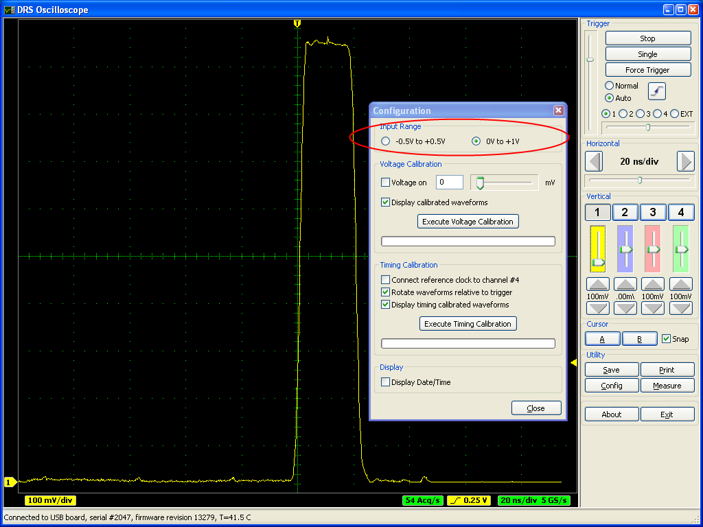
A board firmware update is not necessary for this. It was originally planned to have even a negative range -1V...0V, but this is not possible with the current board design. People who want to record negative pulses have to use an inverter to produce positive pulses. In a future version of the board it might be possible to include this functionality since this is determined by the analog front-end and not the DRS4 chip. |
|
10
|
Tue Jul 7 16:39:57 2009 |
Stefan Ritt | Power up problem and remedy | Maybe some of you have experienced that the DRS4 chip can get pretty hot after power up. After it's initialized the first time, the power consumption goes back to normal. I finally found the cause of this problem and have a remedy. Here is the new paragraph from the updated data sheet:
During power-up, care has to be taken that the DENABLE and DWRITE signals are low. If not, the domino wave can get started before the power supply voltages are stable, which brings the DRS4 chip into a state where it draws a considerable amount of current and heats up significantly. This can be problematic if the signals are directly generated by a FPGA, since most FPGAs have internal pull-up resistors which get activated during the configuration phase of the FPGA. In such a case, the DENABLE and DWRITE signals should be connected to GND with a pull down resistor. This resistor should be much smaller than the FPGA pull-up resistor in order to keep the signals close to GND during the FPGA configuration. A typical value is 4.7 kOhm.
The attached schematics shows the location of the two required resistors. |
| Attachment 1: typical_mode.gif
|

|
|
11
|
Thu Jul 9 09:11:03 2009 |
Stefan Ritt | Current problems with drs_exam.cpp | The current version of the DRS readout example program drs_exam.cpp has two problems:
- The sampling frequency cannot be changed, it will always stay in the region around 5 GSPS
- The waveform obtained by GetWave is rotated such that the first DRS cell corresponds to the first array bin
Both problems have been fixed and the fix will be contained in an upcoming software release. |
|
12
|
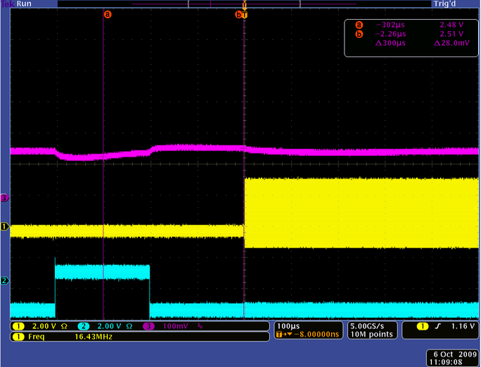
Tue Oct 6 11:20:39 2009 |
Stefan Ritt | VDD instability | It has turned out that the stability of the AVDD and DVDD power supplies for the DRS4 are very critical. On the evaluation board I use a REG1117-2.5, on our VME board I use a ADP3338-2.5 for the DVDD power supply. When the domino wave is started, the power consumption of the DRS4 chip jumps up by ~40 mA, which has to be compensated by the linear regulator. Following screen shot shows what happens:
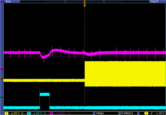
The blue trace is the DWRITE signal indicating the sampling phase when high. The yellow is the SRCLK showing when the readout takes place. The pink is now the DVDD power. It can be clearly seen that there is a dip of ~50 mV when the domino wave starts, a positive dip when it stops and another smaller dip when the readout starts. This causes strange effects: If the trigger arrives during the first dip, the actual sampling takes place when the DVDD is ~50 mV smaller, which leads to a baseline shift of a sampled 0V DC input voltage of about the same amount (-50 mV).
The obvious improvement is to put a huge capacitor on the power supply, but that does not help much:
The dip gets a bit smaller, but it's still there. So a better solution would be to use a faster LDO regulator. Please take care of this if you plan a new design.
Furthermore, I believe that the chip internally has some "warmup" phase, where the die heats up a bit when the additional 40 mA are drawn. So a "good" solution is to wait some time after starting the domino wave until one allows for triggers. Tests showed that a few milliseconds are necessary to keep the baseline shifts below a few millivolts. This of course decreases the dead time of the system significantly, so one has to choose the proper balance between increase dead time and increased base line shift. On some applications where a baseline shift is not an issue, one could opt for the minimum dead time. |
|
13
|
Wed Oct 7 17:58:20 2009 |
Stefan Ritt | VDD switch off speed | It turned out that the VDD switch off speed plays some important role. On our VME board, we have a linear regulator, then a 4.7 uF capacitor, then the DRS4 chip (DVDD and AVDD). When switching off the VME power, it takes quite some time to discharge the 4.7 uF capacitor, since the DRS4 chip goes into a high impedance mode if VDD < ~1V. This gives following VDD trace:
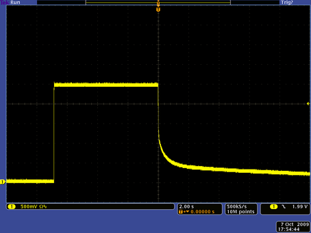
Rising edge is power on, falling edge is power off. Note the horizontal time scale of 2 s/div. So to get below 0.3 V or so, it takes up to 30 seconds. If the power is switched back on when AVDD is above 0.3V, the DRS4 chip can get into a weird state, where probably many domino waves are started and the chip draws an enormous amount of current. Typically the linear regulator limits the current, so the 2.5V drops to ~1.5V, and the board is not working. If people are aware of this and always wait >30sec. before turning the power on again, this is fine, but people might forget.
So the solution is to put a resistor (typically 100 Ohm to 1 kOhm) parallel to the 4.7 uF capacitor in order to have some resistive current load of a few mA. The discharge then looks like this:
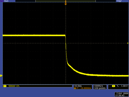
Note the horizontal scale of 10ms/div. So after 30 ms AVDD is discharged and powering on the chip again does not do any harm. The same should be done to DVDD. |
|
14
|
Wed Oct 14 23:53:05 2009 |
Armin Kolb | DRS_exam using USB Evaluation Board with OS X | For the users using a Macintosh,
after several hours the Evaluation Board is working on my Macintosh (intel).
1) install the development package with xcode, its on the OS X installation DVD
2) install the libusb binary from http://www.ellert.se/twain-sane/
3) modify the makefile for compiling drs_exam (attached) afterwards it's running perfect!
best,
Armin
|
| Attachment 1: Makefile
|
########################################################
#
#  Makefile for drs_exam executables
#  under OS X Macintosh with Bash Shell
#
#
########################################################

CFLAGS        = -g -O2 -Wall -Iinclude -DOS_LINUX -DHAVE_LIBUSB
LIBS          = -lpthread -lutil -lusb

CPP_OBJ       = DRS.o
OBJECTS       = musbstd.o mxml.o strlcpy.o

all: drs_exam

drs_exam: $(OBJECTS) DRS.o drs_exam.o
	$(CXX) $(CFLAGS) $(OBJECTS) DRS.o drs_exam.o -o drs_exam $(LIBS)

drs_exam.o: src/drs_exam.cpp include/mxml.h include/DRS.h
	$(CXX) $(CFLAGS) -c $<

$(CPP_OBJ): %.o: src/%.cpp include/%.h include/mxml.h include/DRS.h
	$(CXX) $(CFLAGS) $(WXFLAGS) -c $<

$(OBJECTS): %.o: src/%.c include/mxml.h include/DRS.h
	$(CXX) $(CFLAGS) -c $<

clean:
	rm -f *.o drscl drsosc
|
|
15
|
Fri Oct 16 09:51:03 2009 |
Jinhong Wang | DSR4 Full Readout Mode | Hello Mr. Stefan Ritt
In DSR4 DATASHEET Rev.0.8 Page13, I noticed you metioned the samping should occur after 38 ns after the rising edge of SRCLK when the multiplexer is used. So what is suggested value(delay time between sampling and the rising edge of SRCLK) for the parallel mode,in which the multiplexer is not used?
Best wishes!
Jinhong Wang |
|
16
|
Fri Oct 16 10:16:10 2009 |
Stefan Ritt | DSR4 Full Readout Mode |
| Jinhong Wang wrote: |
|
Hello Mr. Stefan Ritt
In DSR4 DATASHEET Rev.0.8 Page13, I noticed you metioned the samping should occur after 38 ns after the rising edge of SRCLK when the multiplexer is used. So what is suggested value(delay time between sampling and the rising edge of SRCLK) for the parallel mode,in which the multiplexer is not used?
Best wishes!
Jinhong Wang
|
The clock-to-output delay is the same if one uses the multiplexer or not. I found however that in most cases the delay of 38 ns needs some fine tuning to get optimal performance. So I typically use a shifted clock generated by the FPGA clock manager with a programmable delay (+-5 ns for Xilinx) and optimize this in the running system. |
|
17
|
Mon Oct 19 09:06:43 2009 |
Jinhong Wang | BIAS Pin of DRS4 | Dear Mr. Stefan Ritt.
Thank u for your timely response on "DSR4 Full Readout Mode", I received it from Professor Qi An, who is my PhD supervisor.
I am currently going through the DRS4 datasheet. Well, can you give some specification on the usage of "BIAS" pin of DRS4? It is just metioned in the datasheet as bias of internal buffer. What is the internal buffer exactly reffered to here? The MUXOUT buffer of channel 8 or else? Does it have some relationship to O_OFS? I mean, if the reference voltage to BIAS is changed, how will the output be influenced?
Looking forward to hearing from you soon.
Jinhong Wang
Fast Electronics LAB. of University of Science and Technology of China. |
|
18
|
Mon Oct 19 09:13:00 2009 |
Stefan Ritt | BIAS Pin of DRS4 |
| Jinhong Wang wrote: |
|
Dear Mr. Stefan Ritt.
Thank u for your timely response on "DSR4 Full Readout Mode", I received it from Professor Qi An, who is my PhD supervisor.
I am currently going through the DRS4 datasheet. Well, can you give some specification on the usage of "BIAS" pin of DRS4? It is just metioned in the datasheet as bias of internal buffer. What is the internal buffer exactly reffered to here? The MUXOUT buffer of channel 8 or else? Does it have some relationship to O_OFS? I mean, if the reference voltage to BIAS is changed, how will the output be influenced?
Looking forward to hearing from you soon.
Jinhong Wang
Fast Electronics LAB. of University of Science and Technology of China.
|
"internal buffers" are all internal operational amplifiers in the DRS4 chip. Every OPAMP needs a bias (just look it up in any electronics textbook), which determines the linearity and the speed of the OPAMP. When designing DRS4, I was not sure if the required BIAS voltage changes over time, or between chips, so I made it available at a pin, which is a common technique in chip design. But it turns out now that this voltage is not very critical, so just keeping the pin open will work in most cases. |
|
19
|
Mon Oct 19 11:26:29 2009 |
Jinhong Wang | output common mode voltage of DRS4 | Hello Mr. Stifan.Ritt
In the DSR4 datasheet, it is mentioned that there is an additional buffer at each analog output, this buffer shifts the the differential range of -0.5V~0.5V to 0.8V~1.8V. Does it mean that this buffer shifts a voltage of about 1.3V for the primary differential range?
Again for the differential range of -0.5V~0.5V, can the common mode voltage of the analog output at OUT+/OUT- be chaned? In the example presented in the datasheet, OUT+ is 0.8V~1.8V and OUT- is 1.8V~0.8V. So for an output swing of 2V p-p, can the common mode voltage be modified to the desired value? Supposed that the input ranges from -0.5V~0.5V.
Thank you!
Jinhong Wang |
|
20
|
Mon Oct 19 12:46:12 2009 |
Stefan Ritt | output common mode voltage of DRS4 |
| Jinhong Wang wrote: |
|
Does it mean that this buffer shifts a voltage of about 1.3V for the primary differential range?
|
No. It shifts about ROFS-0.25V. So only if ROFS=1.55V, the shift will be 1.3V.
| Jinhong Wang wrote: |
|
Again for the differential range of -0.5V~0.5V, can the common mode voltage of the analog output at OUT+/OUT- be chaned?
|
Just read the datasheet under "ANALOG OUTPUTS". I'm sorry if I did not describe this clearly, but the U+ voltage is fixed (only dependent on ROFS), and U- can be calculated using Uofs as written in the datasheet.
| Jinhong Wang wrote: |
|
In the example presented in the datasheet, OUT+ is 0.8V~1.8V and OUT- is 1.8V~0.8V. So for an output swing of 2V p-p, can the common mode voltage be modified to the desired value? Supposed that the input ranges from -0.5V~0.5V.
|
OUT+ is 0.8V~1.8V, OUT- is 2*Uofs-OUT+. So you can only change the OUT- level, not the OUT+ level. |
|