| ID |
Date |
Author |
Subject |
|
31
|
Sun Jan 31 23:52:15 2010 |
Hao Huan | Failure In Flashing Xilinx PROM | Hi Stefan,
I have an old-version DRS4 evaluation board which doesn't have the latest firmware. I tried to flash the drs_eval1.ipf boundary scan chain into the XCF02S PROM with Xilinx IMPACT, and the firmware seemed to go through into the PROM. However, when I started the DRS command line interface to test the firmware it kept on reporting errors like
musb_write: requested 10, wrote -116, errno 0 (No error)
musb_read error -116
musb_write: requested 10, wrote -22, error 0 (No error)
musb_read error -116
and so on. Finally the program made a dumb recognition of the board as
Found mezz. board 0 on USB, serial #0, firmware revision 0
Do you have any idea which caused this problem? Thanks! |
|
30
|
Mon Jan 11 16:32:21 2010 |
Stefan Ritt | normal_mode_in_drs_exam.cpp |
| aliyilmaz wrote: |
|
Dear Mr. S. Ritt
i am Ms. student , am working with your DRS4 board to calculate the time of flight of the cosmic particle which passes trough the hodoscope . i see the signals at scope , which is negative (i don't want to take positive side of the signal).
i am using your drs_exap.cpp file to take the data, i set the analog trigger source , threshold level is negative, like this(b->SetTriggerLevel(-30, true) ); but the exam file also registers the positive side of signal (i think that is spike or internal reflection), is it possible to eliminate this spike? Also i want to register the data just after the threshold value, but that is always triggered, i think that caused from the mode. Is it possible to set the trigger mode to normal in exam file?,and how can i do that?
Best regards.
Sincerely,
Ali YILMAZ (ali.yilmaz@roma1.infn.it)
|
Please note that SetTriggerLevel(level, polarity) needs "level" in volts, not millivolts, so you need SetTriggerLevel(-0.3, true). The trigger mode is not specified with any library call, but depends on what your program does. If you always poll on IsBusy(), then you are already in "normal" mode. The auto mode can only be achieved on the user application level by doing an "artifical" trigger by calling SoftTrigger() if there are no hardware triggers for a certain time. |
|
29
|
Wed Dec 30 14:28:33 2009 |
aliyilmaz | normal_mode_in_drs_exam.cpp | Dear Mr. S. Ritt
i am Ms. student , am working with your DRS4 board to calculate the time of flight of the cosmic particle which passes trough the hodoscope . i see the signals at scope , which is negative (i don't want to take positive side of the signal).
i am using your drs_exap.cpp file to take the data, i set the analog trigger source , threshold level is negative, like this(b->SetTriggerLevel(-30, true) ); but the exam file also registers the positive side of signal (i think that is spike or internal reflection), is it possible to eliminate this spike? Also i want to register the data just after the threshold value, but that is always triggered, i think that caused from the mode. Is it possible to set the trigger mode to normal in exam file?,and how can i do that?
Best regards.
Sincerely,
Ali YILMAZ (ali.yilmaz@roma1.infn.it)
|
|
28
|
Tue Dec 22 09:07:27 2009 |
Stefan Ritt | Trigger of DRS4 |
| Jinhong Wang wrote: |
|
| Stefan Ritt wrote: |
|
| Jinhong Wang wrote: |
|
| Stefan Ritt wrote: |
|
| Jinhong Wang wrote: |
|
Dear Mr. S. Ritt
The following is my confusion about the trigger of DRS4. It mainly concertrates on the generation of trigger signal to stop DRS4 sampling process for readout of sampled waveform.
As metioned in the datasheet of DRS4, the chip samples the analog input every domino sampling period. After finished sampling a waveform, the sampling process can be stoped by lowering the DWRITE while keeping DENABLE high. But the analog input is asychronous to the Domino CLK. Then, how can we know when to stop the domino sampling process to read out the sampled waveform? Of course, a trigger can be used. But from my present knowledge of DRS4, trigger can only be generated from analog input. Analog input is splited into two channels, one to DRS4 analog input, the other to FPGA as the trigger. However, splitting analog inputs increases the system design complexity, and may lower the total performace. So what is your suggestion?
In our system, there are 8 analog inputs to a signal DRS4 chip, the outputs of DRS4 chip are connected to an 8-channel 14 bit ADC ( AD9252). It wold be kind of you to inform me about the most applicable approach for readout of DRS4 sampled wavefrom.
Best regards.
Sincerely,
Jinhong Wang (wangjinh@mail.ustc.edu.cn)
|
Indeed you have to make an external trigger. The evaluation board uses the "transparent mode" of the DRS4 to "mirror" the input signal at the output, then puts a comparator there. The schematics of the evaluation board is in the manual. This does then not degrate the analog performance. You can of course also split the signal at the input, this will only add a minor additional load to the input signal, since the load of the DRS4 chips itself is much bigger than that of any comparator.
An alternative is to turn on the transparent mode and continuously digitize all 8 outputs with your AD9252. Then you make the trigger purely digital in your FPGA. You can put there a comparator, or even more complex logic like multiplicity etc. Note however that this causes some latency, since the ADC has a pipeline which is quite long, so you have to buffer the latency of your trigger in the analog window of the DRS4 sampling cells. Like if you run the DRS4 at 1 GSPS, you can accomodate 1024 ns of sampling depth, which is good for maybe 500 ns of trigger latency plus 500 ns of the waveform of interest.
|
Thank you. The transparent mode can be really helpful. Can you provide me in more details of the chip's transparent mode? I am still confused about the following aspects.
I notice that DRS4 samples the analog wave in the way "clear before write", and in the transparent mode, there will be certain delay before the trigger logic stops the sampling process. So,does it mean that the waveform recording process per Domino sampling cycle will not degrade the amplitude of the analog signal? Hence, for two idential analog inputs, one with a trigger latency of 500 ns and the other of 510 ns, the sampled waveform is identical, what differs is the starting number of the first active sampling cell, where the reading process considered to be started. Is that right? Looking forward to your insight.
Best regrads.
Sincerely,
Jinhong Wang (wangjinh@mail.ustc.edu.cn)
|
The amplitude of the analog signal is not degraded by the transparent mode, since the signal is buffered on the chip, and the output of this buffer is send off the chip. The waveform digitizing of course requires quite some current to charge up all capacitors, so there is maximum current of ~1mA for 5 GSPS. If you only have a weak signal source, your bandwidth might be limited by that. On the evaluation board for example we use passive transformers to produce the differential input signal from a single-ended signal. Although the transformers are rated 1 GHz Bandwidth, we only achieve 200 MHz with the passive transformers. By using active high speed differential drivers, you can get about 700 MHz right now.
If you have two channels with 500 ns and 510 ns trigger latency, there is no difference in the "domino stop position" since there is only one domino circuit per chip which can be stopped. So the stop position is the same for all eight channels on a chip.
|
So you mean there is an analog buffer per channel? The analog signal is buffered there, before entering the sampling cells? Then, when will the buffer content be released and cleared? How shall I handle "Dwite" and "Denable" during a complete operation when an analog signal arrives in the transparent mode? I cannot find more information beyond the datasheet, a detailed description of the transparent mode (and the analog buffer, if possible) will be really helpful for me.
Best,
Sincerely,
Jinhong Wang (wangjinh@mail.ustc.edu.cn)
|
There is one analog buffer per channel at the output, as indicated on the FUNCTIONAL BLOCK DIAGRAM of the datasheet. The section ANALOG INPUTS clearly states that the input signal has to load directly the sampling capacitors.
All other people using the chip so far correctly understood these things so far, so I believe more information beyond the datasheet is not necessary. I believe you have a principal problem of understanding, which can hardly be clarified by email. Best would be if you directly call me, I can then explain things to you. |
|
27
|
Tue Dec 22 01:30:55 2009 |
Jinhong Wang | Trigger of DRS4 |
| Stefan Ritt wrote: |
|
| Jinhong Wang wrote: |
|
| Stefan Ritt wrote: |
|
| Jinhong Wang wrote: |
|
Dear Mr. S. Ritt
The following is my confusion about the trigger of DRS4. It mainly concertrates on the generation of trigger signal to stop DRS4 sampling process for readout of sampled waveform.
As metioned in the datasheet of DRS4, the chip samples the analog input every domino sampling period. After finished sampling a waveform, the sampling process can be stoped by lowering the DWRITE while keeping DENABLE high. But the analog input is asychronous to the Domino CLK. Then, how can we know when to stop the domino sampling process to read out the sampled waveform? Of course, a trigger can be used. But from my present knowledge of DRS4, trigger can only be generated from analog input. Analog input is splited into two channels, one to DRS4 analog input, the other to FPGA as the trigger. However, splitting analog inputs increases the system design complexity, and may lower the total performace. So what is your suggestion?
In our system, there are 8 analog inputs to a signal DRS4 chip, the outputs of DRS4 chip are connected to an 8-channel 14 bit ADC ( AD9252). It wold be kind of you to inform me about the most applicable approach for readout of DRS4 sampled wavefrom.
Best regards.
Sincerely,
Jinhong Wang (wangjinh@mail.ustc.edu.cn)
|
Indeed you have to make an external trigger. The evaluation board uses the "transparent mode" of the DRS4 to "mirror" the input signal at the output, then puts a comparator there. The schematics of the evaluation board is in the manual. This does then not degrate the analog performance. You can of course also split the signal at the input, this will only add a minor additional load to the input signal, since the load of the DRS4 chips itself is much bigger than that of any comparator.
An alternative is to turn on the transparent mode and continuously digitize all 8 outputs with your AD9252. Then you make the trigger purely digital in your FPGA. You can put there a comparator, or even more complex logic like multiplicity etc. Note however that this causes some latency, since the ADC has a pipeline which is quite long, so you have to buffer the latency of your trigger in the analog window of the DRS4 sampling cells. Like if you run the DRS4 at 1 GSPS, you can accomodate 1024 ns of sampling depth, which is good for maybe 500 ns of trigger latency plus 500 ns of the waveform of interest.
|
Thank you. The transparent mode can be really helpful. Can you provide me in more details of the chip's transparent mode? I am still confused about the following aspects.
I notice that DRS4 samples the analog wave in the way "clear before write", and in the transparent mode, there will be certain delay before the trigger logic stops the sampling process. So,does it mean that the waveform recording process per Domino sampling cycle will not degrade the amplitude of the analog signal? Hence, for two idential analog inputs, one with a trigger latency of 500 ns and the other of 510 ns, the sampled waveform is identical, what differs is the starting number of the first active sampling cell, where the reading process considered to be started. Is that right? Looking forward to your insight.
Best regrads.
Sincerely,
Jinhong Wang (wangjinh@mail.ustc.edu.cn)
|
The amplitude of the analog signal is not degraded by the transparent mode, since the signal is buffered on the chip, and the output of this buffer is send off the chip. The waveform digitizing of course requires quite some current to charge up all capacitors, so there is maximum current of ~1mA for 5 GSPS. If you only have a weak signal source, your bandwidth might be limited by that. On the evaluation board for example we use passive transformers to produce the differential input signal from a single-ended signal. Although the transformers are rated 1 GHz Bandwidth, we only achieve 200 MHz with the passive transformers. By using active high speed differential drivers, you can get about 700 MHz right now.
If you have two channels with 500 ns and 510 ns trigger latency, there is no difference in the "domino stop position" since there is only one domino circuit per chip which can be stopped. So the stop position is the same for all eight channels on a chip.
|
So you mean there is an analog buffer per channel? The analog signal is buffered there, before entering the sampling cells? Then, when will the buffer content be released and cleared? How shall I handle "Dwite" and "Denable" during a complete operation when an analog signal arrives in the transparent mode? I cannot find more information beyond the datasheet, a detailed description of the transparent mode (and the analog buffer, if possible) will be really helpful for me.
Best,
Sincerely,
Jinhong Wang (wangjinh@mail.ustc.edu.cn) |
|
26
|
Mon Dec 21 16:52:08 2009 |
Stefan Ritt | Trigger of DRS4 |
| Jinhong Wang wrote: |
|
| Stefan Ritt wrote: |
|
| Jinhong Wang wrote: |
|
Dear Mr. S. Ritt
The following is my confusion about the trigger of DRS4. It mainly concertrates on the generation of trigger signal to stop DRS4 sampling process for readout of sampled waveform.
As metioned in the datasheet of DRS4, the chip samples the analog input every domino sampling period. After finished sampling a waveform, the sampling process can be stoped by lowering the DWRITE while keeping DENABLE high. But the analog input is asychronous to the Domino CLK. Then, how can we know when to stop the domino sampling process to read out the sampled waveform? Of course, a trigger can be used. But from my present knowledge of DRS4, trigger can only be generated from analog input. Analog input is splited into two channels, one to DRS4 analog input, the other to FPGA as the trigger. However, splitting analog inputs increases the system design complexity, and may lower the total performace. So what is your suggestion?
In our system, there are 8 analog inputs to a signal DRS4 chip, the outputs of DRS4 chip are connected to an 8-channel 14 bit ADC ( AD9252). It wold be kind of you to inform me about the most applicable approach for readout of DRS4 sampled wavefrom.
Best regards.
Sincerely,
Jinhong Wang (wangjinh@mail.ustc.edu.cn)
|
Indeed you have to make an external trigger. The evaluation board uses the "transparent mode" of the DRS4 to "mirror" the input signal at the output, then puts a comparator there. The schematics of the evaluation board is in the manual. This does then not degrate the analog performance. You can of course also split the signal at the input, this will only add a minor additional load to the input signal, since the load of the DRS4 chips itself is much bigger than that of any comparator.
An alternative is to turn on the transparent mode and continuously digitize all 8 outputs with your AD9252. Then you make the trigger purely digital in your FPGA. You can put there a comparator, or even more complex logic like multiplicity etc. Note however that this causes some latency, since the ADC has a pipeline which is quite long, so you have to buffer the latency of your trigger in the analog window of the DRS4 sampling cells. Like if you run the DRS4 at 1 GSPS, you can accomodate 1024 ns of sampling depth, which is good for maybe 500 ns of trigger latency plus 500 ns of the waveform of interest.
|
Thank you. The transparent mode can be really helpful. Can you provide me in more details of the chip's transparent mode? I am still confused about the following aspects.
I notice that DRS4 samples the analog wave in the way "clear before write", and in the transparent mode, there will be certain delay before the trigger logic stops the sampling process. So,does it mean that the waveform recording process per Domino sampling cycle will not degrade the amplitude of the analog signal? Hence, for two idential analog inputs, one with a trigger latency of 500 ns and the other of 510 ns, the sampled waveform is identical, what differs is the starting number of the first active sampling cell, where the reading process considered to be started. Is that right? Looking forward to your insight.
Best regrads.
Sincerely,
Jinhong Wang (wangjinh@mail.ustc.edu.cn)
|
The amplitude of the analog signal is not degraded by the transparent mode, since the signal is buffered on the chip, and the output of this buffer is send off the chip. The waveform digitizing of course requires quite some current to charge up all capacitors, so there is maximum current of ~1mA for 5 GSPS. If you only have a weak signal source, your bandwidth might be limited by that. On the evaluation board for example we use passive transformers to produce the differential input signal from a single-ended signal. Although the transformers are rated 1 GHz Bandwidth, we only achieve 200 MHz with the passive transformers. By using active high speed differential drivers, you can get about 700 MHz right now.
If you have two channels with 500 ns and 510 ns trigger latency, there is no difference in the "domino stop position" since there is only one domino circuit per chip which can be stopped. So the stop position is the same for all eight channels on a chip. |
|
25
|
Mon Dec 21 10:17:05 2009 |
Jinhong Wang | Trigger of DRS4 |
| Stefan Ritt wrote: |
|
| Jinhong Wang wrote: |
|
Dear Mr. S. Ritt
The following is my confusion about the trigger of DRS4. It mainly concertrates on the generation of trigger signal to stop DRS4 sampling process for readout of sampled waveform.
As metioned in the datasheet of DRS4, the chip samples the analog input every domino sampling period. After finished sampling a waveform, the sampling process can be stoped by lowering the DWRITE while keeping DENABLE high. But the analog input is asychronous to the Domino CLK. Then, how can we know when to stop the domino sampling process to read out the sampled waveform? Of course, a trigger can be used. But from my present knowledge of DRS4, trigger can only be generated from analog input. Analog input is splited into two channels, one to DRS4 analog input, the other to FPGA as the trigger. However, splitting analog inputs increases the system design complexity, and may lower the total performace. So what is your suggestion?
In our system, there are 8 analog inputs to a signal DRS4 chip, the outputs of DRS4 chip are connected to an 8-channel 14 bit ADC ( AD9252). It wold be kind of you to inform me about the most applicable approach for readout of DRS4 sampled wavefrom.
Best regards.
Sincerely,
Jinhong Wang (wangjinh@mail.ustc.edu.cn)
|
Indeed you have to make an external trigger. The evaluation board uses the "transparent mode" of the DRS4 to "mirror" the input signal at the output, then puts a comparator there. The schematics of the evaluation board is in the manual. This does then not degrate the analog performance. You can of course also split the signal at the input, this will only add a minor additional load to the input signal, since the load of the DRS4 chips itself is much bigger than that of any comparator.
An alternative is to turn on the transparent mode and continuously digitize all 8 outputs with your AD9252. Then you make the trigger purely digital in your FPGA. You can put there a comparator, or even more complex logic like multiplicity etc. Note however that this causes some latency, since the ADC has a pipeline which is quite long, so you have to buffer the latency of your trigger in the analog window of the DRS4 sampling cells. Like if you run the DRS4 at 1 GSPS, you can accomodate 1024 ns of sampling depth, which is good for maybe 500 ns of trigger latency plus 500 ns of the waveform of interest.
|
Thank you. The transparent mode can be really helpful. Can you provide me in more details of the chip's transparent mode? I am still confused about the following aspects.
I notice that DRS4 samples the analog wave in the way "clear before write", and in the transparent mode, there will be certain delay before the trigger logic stops the sampling process. So,does it mean that the waveform recording process per Domino sampling cycle will not degrade the amplitude of the analog signal? Hence, for two idential analog inputs, one with a trigger latency of 500 ns and the other of 510 ns, the sampled waveform is identical, what differs is the starting number of the first active sampling cell, where the reading process considered to be started. Is that right? Looking forward to your insight.
Best regrads.
Sincerely,
Jinhong Wang (wangjinh@mail.ustc.edu.cn) |
|
24
|
Tue Dec 15 14:38:09 2009 |
Stefan Ritt | Trigger of DRS4 |
| Jinhong Wang wrote: |
|
Dear Mr. S. Ritt
The following is my confusion about the trigger of DRS4. It mainly concertrates on the generation of trigger signal to stop DRS4 sampling process for readout of sampled waveform.
As metioned in the datasheet of DRS4, the chip samples the analog input every domino sampling period. After finished sampling a waveform, the sampling process can be stoped by lowering the DWRITE while keeping DENABLE high. But the analog input is asychronous to the Domino CLK. Then, how can we know when to stop the domino sampling process to read out the sampled waveform? Of course, a trigger can be used. But from my present knowledge of DRS4, trigger can only be generated from analog input. Analog input is splited into two channels, one to DRS4 analog input, the other to FPGA as the trigger. However, splitting analog inputs increases the system design complexity, and may lower the total performace. So what is your suggestion?
In our system, there are 8 analog inputs to a signal DRS4 chip, the outputs of DRS4 chip are connected to an 8-channel 14 bit ADC ( AD9252). It wold be kind of you to inform me about the most applicable approach for readout of DRS4 sampled wavefrom.
Best regards.
Sincerely,
Jinhong Wang (wangjinh@mail.ustc.edu.cn)
|
Indeed you have to make an external trigger. The evaluation board uses the "transparent mode" of the DRS4 to "mirror" the input signal at the output, then puts a comparator there. The schematics of the evaluation board is in the manual. This does then not degrate the analog performance. You can of course also split the signal at the input, this will only add a minor additional load to the input signal, since the load of the DRS4 chips itself is much bigger than that of any comparator.
An alternative is to turn on the transparent mode and continuously digitize all 8 outputs with your AD9252. Then you make the trigger purely digital in your FPGA. You can put there a comparator, or even more complex logic like multiplicity etc. Note however that this causes some latency, since the ADC has a pipeline which is quite long, so you have to buffer the latency of your trigger in the analog window of the DRS4 sampling cells. Like if you run the DRS4 at 1 GSPS, you can accomodate 1024 ns of sampling depth, which is good for maybe 500 ns of trigger latency plus 500 ns of the waveform of interest. |
|
23
|
Mon Dec 14 10:14:16 2009 |
Jinhong Wang | Trigger of DRS4 | Dear Mr. S. Ritt
The following is my confusion about the trigger of DRS4. It mainly concertrates on the generation of trigger signal to stop DRS4 sampling process for readout of sampled waveform.
As metioned in the datasheet of DRS4, the chip samples the analog input every domino sampling period. After finished sampling a waveform, the sampling process can be stoped by lowering the DWRITE while keeping DENABLE high. But the analog input is asychronous to the Domino CLK. Then, how can we know when to stop the domino sampling process to read out the sampled waveform? Of course, a trigger can be used. But from my present knowledge of DRS4, trigger can only be generated from analog input. Analog input is splited into two channels, one to DRS4 analog input, the other to FPGA as the trigger. However, splitting analog inputs increases the system design complexity, and may lower the total performace. So what is your suggestion?
In our system, there are 8 analog inputs to a signal DRS4 chip, the outputs of DRS4 chip are connected to an 8-channel 14 bit ADC ( AD9252). It wold be kind of you to inform me about the most applicable approach for readout of DRS4 sampled wavefrom.
Best regards.
Sincerely,
Jinhong Wang (wangjinh@mail.ustc.edu.cn) |
|
22
|
Wed Nov 4 14:42:22 2009 |
Stefan Ritt | outline dimension of DRS4 |
| Jinhong Wang wrote: |
|
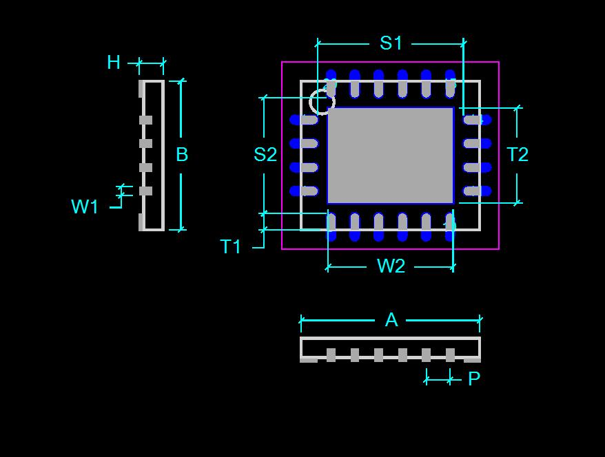
Fig.1 typical dimension of QFN package
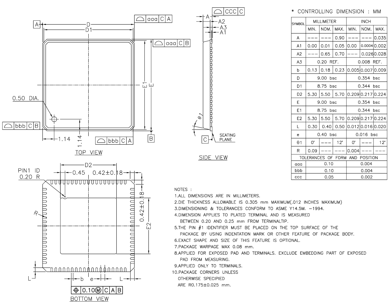
Above is the typical dimension specification for QFN package. I cann't find the corresponding "T1" as in Fig.1 in the DRS4 documents, nor any of the tolerance of the dimensions, which are usually expressed in the form of a range between a min. value and a max. value.
So will you specify the dimension of "T1" and "W1", and the dimension tolerance of them?
Thanks and best wishes!
Jinhong Wang University of Science and Technology of China
|
Please find attached the complete dimensions. |
| Attachment 1: qfn76.png
|
|
|
21
|
Fri Oct 30 03:31:54 2009 |
Jinhong Wang | outline dimension of DRS4 | 
Fig.1 typical dimension of QFN package
Above is the typical dimension specification for QFN package. I cann't find the corresponding "T1" as in Fig.1 in the DRS4 documents, nor any of the tolerance of the dimensions, which are usually expressed in the form of a range between a min. value and a max. value.
So will you specify the dimension of "T1" and "W1", and the dimension tolerance of them?
Thanks and best wishes!
Jinhong Wang University of Science and Technology of China |
|
20
|
Mon Oct 19 12:46:12 2009 |
Stefan Ritt | output common mode voltage of DRS4 |
| Jinhong Wang wrote: |
|
Does it mean that this buffer shifts a voltage of about 1.3V for the primary differential range?
|
No. It shifts about ROFS-0.25V. So only if ROFS=1.55V, the shift will be 1.3V.
| Jinhong Wang wrote: |
|
Again for the differential range of -0.5V~0.5V, can the common mode voltage of the analog output at OUT+/OUT- be chaned?
|
Just read the datasheet under "ANALOG OUTPUTS". I'm sorry if I did not describe this clearly, but the U+ voltage is fixed (only dependent on ROFS), and U- can be calculated using Uofs as written in the datasheet.
| Jinhong Wang wrote: |
|
In the example presented in the datasheet, OUT+ is 0.8V~1.8V and OUT- is 1.8V~0.8V. So for an output swing of 2V p-p, can the common mode voltage be modified to the desired value? Supposed that the input ranges from -0.5V~0.5V.
|
OUT+ is 0.8V~1.8V, OUT- is 2*Uofs-OUT+. So you can only change the OUT- level, not the OUT+ level. |
|
19
|
Mon Oct 19 11:26:29 2009 |
Jinhong Wang | output common mode voltage of DRS4 | Hello Mr. Stifan.Ritt
In the DSR4 datasheet, it is mentioned that there is an additional buffer at each analog output, this buffer shifts the the differential range of -0.5V~0.5V to 0.8V~1.8V. Does it mean that this buffer shifts a voltage of about 1.3V for the primary differential range?
Again for the differential range of -0.5V~0.5V, can the common mode voltage of the analog output at OUT+/OUT- be chaned? In the example presented in the datasheet, OUT+ is 0.8V~1.8V and OUT- is 1.8V~0.8V. So for an output swing of 2V p-p, can the common mode voltage be modified to the desired value? Supposed that the input ranges from -0.5V~0.5V.
Thank you!
Jinhong Wang |
|
18
|
Mon Oct 19 09:13:00 2009 |
Stefan Ritt | BIAS Pin of DRS4 |
| Jinhong Wang wrote: |
|
Dear Mr. Stefan Ritt.
Thank u for your timely response on "DSR4 Full Readout Mode", I received it from Professor Qi An, who is my PhD supervisor.
I am currently going through the DRS4 datasheet. Well, can you give some specification on the usage of "BIAS" pin of DRS4? It is just metioned in the datasheet as bias of internal buffer. What is the internal buffer exactly reffered to here? The MUXOUT buffer of channel 8 or else? Does it have some relationship to O_OFS? I mean, if the reference voltage to BIAS is changed, how will the output be influenced?
Looking forward to hearing from you soon.
Jinhong Wang
Fast Electronics LAB. of University of Science and Technology of China.
|
"internal buffers" are all internal operational amplifiers in the DRS4 chip. Every OPAMP needs a bias (just look it up in any electronics textbook), which determines the linearity and the speed of the OPAMP. When designing DRS4, I was not sure if the required BIAS voltage changes over time, or between chips, so I made it available at a pin, which is a common technique in chip design. But it turns out now that this voltage is not very critical, so just keeping the pin open will work in most cases. |
|
17
|
Mon Oct 19 09:06:43 2009 |
Jinhong Wang | BIAS Pin of DRS4 | Dear Mr. Stefan Ritt.
Thank u for your timely response on "DSR4 Full Readout Mode", I received it from Professor Qi An, who is my PhD supervisor.
I am currently going through the DRS4 datasheet. Well, can you give some specification on the usage of "BIAS" pin of DRS4? It is just metioned in the datasheet as bias of internal buffer. What is the internal buffer exactly reffered to here? The MUXOUT buffer of channel 8 or else? Does it have some relationship to O_OFS? I mean, if the reference voltage to BIAS is changed, how will the output be influenced?
Looking forward to hearing from you soon.
Jinhong Wang
Fast Electronics LAB. of University of Science and Technology of China. |
|
16
|
Fri Oct 16 10:16:10 2009 |
Stefan Ritt | DSR4 Full Readout Mode |
| Jinhong Wang wrote: |
|
Hello Mr. Stefan Ritt
In DSR4 DATASHEET Rev.0.8 Page13, I noticed you metioned the samping should occur after 38 ns after the rising edge of SRCLK when the multiplexer is used. So what is suggested value(delay time between sampling and the rising edge of SRCLK) for the parallel mode,in which the multiplexer is not used?
Best wishes!
Jinhong Wang
|
The clock-to-output delay is the same if one uses the multiplexer or not. I found however that in most cases the delay of 38 ns needs some fine tuning to get optimal performance. So I typically use a shifted clock generated by the FPGA clock manager with a programmable delay (+-5 ns for Xilinx) and optimize this in the running system. |
|
15
|
Fri Oct 16 09:51:03 2009 |
Jinhong Wang | DSR4 Full Readout Mode | Hello Mr. Stefan Ritt
In DSR4 DATASHEET Rev.0.8 Page13, I noticed you metioned the samping should occur after 38 ns after the rising edge of SRCLK when the multiplexer is used. So what is suggested value(delay time between sampling and the rising edge of SRCLK) for the parallel mode,in which the multiplexer is not used?
Best wishes!
Jinhong Wang |
|
14
|
Wed Oct 14 23:53:05 2009 |
Armin Kolb | DRS_exam using USB Evaluation Board with OS X | For the users using a Macintosh,
after several hours the Evaluation Board is working on my Macintosh (intel).
1) install the development package with xcode, its on the OS X installation DVD
2) install the libusb binary from http://www.ellert.se/twain-sane/
3) modify the makefile for compiling drs_exam (attached) afterwards it's running perfect!
best,
Armin
|
| Attachment 1: Makefile
|
########################################################
#
#  Makefile for drs_exam executables
#  under OS X Macintosh with Bash Shell
#
#
########################################################

CFLAGS        = -g -O2 -Wall -Iinclude -DOS_LINUX -DHAVE_LIBUSB
LIBS          = -lpthread -lutil -lusb

CPP_OBJ       = DRS.o
OBJECTS       = musbstd.o mxml.o strlcpy.o

all: drs_exam

drs_exam: $(OBJECTS) DRS.o drs_exam.o
	$(CXX) $(CFLAGS) $(OBJECTS) DRS.o drs_exam.o -o drs_exam $(LIBS)

drs_exam.o: src/drs_exam.cpp include/mxml.h include/DRS.h
	$(CXX) $(CFLAGS) -c $<

$(CPP_OBJ): %.o: src/%.cpp include/%.h include/mxml.h include/DRS.h
	$(CXX) $(CFLAGS) $(WXFLAGS) -c $<

$(OBJECTS): %.o: src/%.c include/mxml.h include/DRS.h
	$(CXX) $(CFLAGS) -c $<

clean:
	rm -f *.o drscl drsosc
|
|
13
|
Wed Oct 7 17:58:20 2009 |
Stefan Ritt | VDD switch off speed | It turned out that the VDD switch off speed plays some important role. On our VME board, we have a linear regulator, then a 4.7 uF capacitor, then the DRS4 chip (DVDD and AVDD). When switching off the VME power, it takes quite some time to discharge the 4.7 uF capacitor, since the DRS4 chip goes into a high impedance mode if VDD < ~1V. This gives following VDD trace:
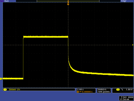
Rising edge is power on, falling edge is power off. Note the horizontal time scale of 2 s/div. So to get below 0.3 V or so, it takes up to 30 seconds. If the power is switched back on when AVDD is above 0.3V, the DRS4 chip can get into a weird state, where probably many domino waves are started and the chip draws an enormous amount of current. Typically the linear regulator limits the current, so the 2.5V drops to ~1.5V, and the board is not working. If people are aware of this and always wait >30sec. before turning the power on again, this is fine, but people might forget.
So the solution is to put a resistor (typically 100 Ohm to 1 kOhm) parallel to the 4.7 uF capacitor in order to have some resistive current load of a few mA. The discharge then looks like this:
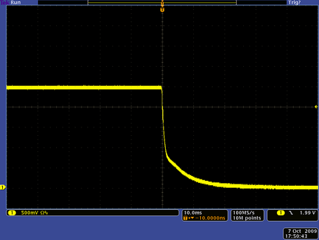
Note the horizontal scale of 10ms/div. So after 30 ms AVDD is discharged and powering on the chip again does not do any harm. The same should be done to DVDD. |
|
12
|
Tue Oct 6 11:20:39 2009 |
Stefan Ritt | VDD instability | It has turned out that the stability of the AVDD and DVDD power supplies for the DRS4 are very critical. On the evaluation board I use a REG1117-2.5, on our VME board I use a ADP3338-2.5 for the DVDD power supply. When the domino wave is started, the power consumption of the DRS4 chip jumps up by ~40 mA, which has to be compensated by the linear regulator. Following screen shot shows what happens:
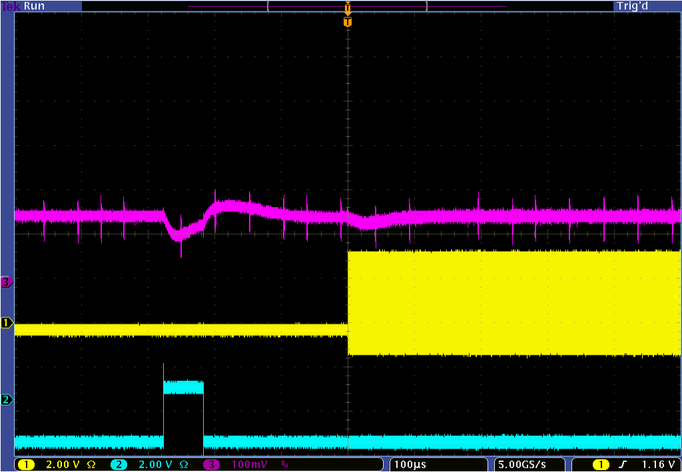
The blue trace is the DWRITE signal indicating the sampling phase when high. The yellow is the SRCLK showing when the readout takes place. The pink is now the DVDD power. It can be clearly seen that there is a dip of ~50 mV when the domino wave starts, a positive dip when it stops and another smaller dip when the readout starts. This causes strange effects: If the trigger arrives during the first dip, the actual sampling takes place when the DVDD is ~50 mV smaller, which leads to a baseline shift of a sampled 0V DC input voltage of about the same amount (-50 mV).
The obvious improvement is to put a huge capacitor on the power supply, but that does not help much:
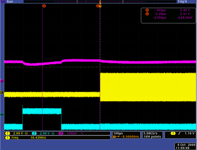
The dip gets a bit smaller, but it's still there. So a better solution would be to use a faster LDO regulator. Please take care of this if you plan a new design.
Furthermore, I believe that the chip internally has some "warmup" phase, where the die heats up a bit when the additional 40 mA are drawn. So a "good" solution is to wait some time after starting the domino wave until one allows for triggers. Tests showed that a few milliseconds are necessary to keep the baseline shifts below a few millivolts. This of course decreases the dead time of the system significantly, so one has to choose the proper balance between increase dead time and increased base line shift. On some applications where a baseline shift is not an issue, one could opt for the minimum dead time. |
|