 Fri Mar 11 17:26:15 2022, Matias Senger, Time calibration and the C++ API Fri Mar 11 17:26:15 2022, Matias Senger, Time calibration and the C++ API
|
I am using the V5 board at a fixed sampling frequency. With the `drsosc` app I have executed the time calibration at 5 GS/s (actually 5.12 GS/s). This is how my setup looks like in the app:

Now I want to replicate this using the C++ API (not the positive width measurement shown, the signal sampling only). I am seting the sampling frequency to 5 GS/s, as I do in the `drsosc` app. Then I get the time information using the `DRSBoard::GetTime(unsigned int chipIndex, int channelIndex, int tc, float *time)` function (which I don't find defined either in `DRS.h` or `DRS.cpp` but somehow it works). How can I know if these times that I get here are being corrected with the time calibration? If so, should I expect the time resolution to be < 3 ps? Are these 3 ps accumulative, such that in the end I end up having a contribution from the evaluation board of 3 ps × 5 Gs/s × 100 ns where 100 ns is the time difference between my two pulses? (This does not seem to be the case because if so I would expect the jitter to be ~ 1 ns, and we see that the "Pos Width" measurement is ~ 0.1 ns std.)
Why am I asking? I want to measure the jitter between the two falling edges. This cannot be done easily with the `drsosc` app I think, so I am acquiring the data and doing this offline. I have done this measurement in the past using a LeCroy WaveRunner oscilloscope with 20 GS/s and 4 GHz bandwidth (offline, same code) and I have seen it vary from ~5 ps → 30 ps when I vary a voltage that I can control. Now if I calculate this time fluctuation using the data acquired with the V5 evaluation board I get a value ~100 ps and independent of this voltage, which leads me to conclude that the limiting factor is being the evaluation board itself. So now I am wondering if I have reached its limit, or if there is some setting that can still improve this result.
Thanks! |
 Sat Mar 12 10:13:24 2022, Stefan Ritt, Time calibration and the C++ API Sat Mar 12 10:13:24 2022, Stefan Ritt, Time calibration and the C++ API
|
DRSBoard::GetTime is declared in DRS.h line 720.
If you want to measure timing down to ps, you need some basic knowledge, especially about signal-to-noise and risetime. This cannot be taught in a few sentenses, needs a full lecture. As a starting point please read that papat:
https://arxiv.org/abs/1405.4975
then you will understand why you measure different resolutions with different peak heights (and different rise times).
Concerning the DRS4 measurement, please be aware that the sampling poings are not equidistant, like not every 200ps for GSPS. They vary bin by bin significantly, from 50ps to 300ps. So you alway have to analyse the X/Y points as an array, not just the Y values assuming deltaX of 200ps. Probably you forgot that. Then, you have to interpolate between bins to find the crossing over your threshold. Linear interpolation is already good, spline interpolation even better. Deep inside Measurement.cpp of the drsosc program you find in the source code:
t1 = (thr*(x1[i]-x1[i-1])+x1[i-1]*y1[i]-x1[i]*y1[i-1])/(y1[i]-y1[i-1]);
which is the linear interpolation (thr is the threshold). You have to use (and understand!) similar code.
Best,
Stefan
| Matias Senger wrote: |
|
I am using the V5 board at a fixed sampling frequency. With the `drsosc` app I have executed the time calibration at 5 GS/s (actually 5.12 GS/s). This is how my setup looks like in the app:
Now I want to replicate this using the C++ API (not the positive width measurement shown, the signal sampling only). I am seting the sampling frequency to 5 GS/s, as I do in the `drsosc` app. Then I get the time information using the `DRSBoard::GetTime(unsigned int chipIndex, int channelIndex, int tc, float *time)` function (which I don't find defined either in `DRS.h` or `DRS.cpp` but somehow it works). How can I know if these times that I get here are being corrected with the time calibration? If so, should I expect the time resolution to be < 3 ps? Are these 3 ps accumulative, such that in the end I end up having a contribution from the evaluation board of 3 ps × 5 Gs/s × 100 ns where 100 ns is the time difference between my two pulses? (This does not seem to be the case because if so I would expect the jitter to be ~ 1 ns, and we see that the "Pos Width" measurement is ~ 0.1 ns std.)
Why am I asking? I want to measure the jitter between the two falling edges. This cannot be done easily with the `drsosc` app I think, so I am acquiring the data and doing this offline. I have done this measurement in the past using a LeCroy WaveRunner oscilloscope with 20 GS/s and 4 GHz bandwidth (offline, same code) and I have seen it vary from ~5 ps → 30 ps when I vary a voltage that I can control. Now if I calculate this time fluctuation using the data acquired with the V5 evaluation board I get a value ~100 ps and independent of this voltage, which leads me to conclude that the limiting factor is being the evaluation board itself. So now I am wondering if I have reached its limit, or if there is some setting that can still improve this result.
Thanks!
|
|
|
Sat Mar 12 16:52:36 2022, Matias Senger, Time calibration and the C++ API
|
Dear Stefan,
For the time of each bin I am using the values returend by `GetTime` without any assumption by my side. I did not notice before that the sampling time is not uniform, but I see that this is already happening. This is an example plot from one of the signals I processed:

The bin at 65.5 ns and the next one are closer than their neighbors. So this seems to indicate that the time calibration is being taken into account when I acquire the time bins using `GetTime`, is this correct?
To obtain the final time resolution I am using the constant fraction discriminator method and the signals are linearly interpolated to obtain the time at each percentage value, as seen in the plot. I have already measured time resolutions in the 5-100 ps range with exactly the same setup but using the LeCroy oscilloscope, which I am using just for data acquisition, and my software for offline analysis as shown in the plot above. Now what I am trying to do is to replace the LeCroy by the DRS4 Evaluation Board basically, so I can use the oscilloscope in a different setup.
Best,
Matias.
| Stefan Ritt wrote: |
|
DRSBoard::GetTime is declared in DRS.h line 720.
If you want to measure timing down to ps, you need some basic knowledge, especially about signal-to-noise and risetime. This cannot be taught in a few sentenses, needs a full lecture. As a starting point please read that papat:
https://arxiv.org/abs/1405.4975
then you will understand why you measure different resolutions with different peak heights (and different rise times).
Concerning the DRS4 measurement, please be aware that the sampling poings are not equidistant, like not every 200ps for GSPS. They vary bin by bin significantly, from 50ps to 300ps. So you alway have to analyse the X/Y points as an array, not just the Y values assuming deltaX of 200ps. Probably you forgot that. Then, you have to interpolate between bins to find the crossing over your threshold. Linear interpolation is already good, spline interpolation even better. Deep inside Measurement.cpp of the drsosc program you find in the source code:
t1 = (thr*(x1[i]-x1[i-1])+x1[i-1]*y1[i]-x1[i]*y1[i-1])/(y1[i]-y1[i-1]);
which is the linear interpolation (thr is the threshold). You have to use (and understand!) similar code.
Best,
Stefan
| Matias Senger wrote: |
|
I am using the V5 board at a fixed sampling frequency. With the `drsosc` app I have executed the time calibration at 5 GS/s (actually 5.12 GS/s). This is how my setup looks like in the app:
Now I want to replicate this using the C++ API (not the positive width measurement shown, the signal sampling only). I am seting the sampling frequency to 5 GS/s, as I do in the `drsosc` app. Then I get the time information using the `DRSBoard::GetTime(unsigned int chipIndex, int channelIndex, int tc, float *time)` function (which I don't find defined either in `DRS.h` or `DRS.cpp` but somehow it works). How can I know if these times that I get here are being corrected with the time calibration? If so, should I expect the time resolution to be < 3 ps? Are these 3 ps accumulative, such that in the end I end up having a contribution from the evaluation board of 3 ps × 5 Gs/s × 100 ns where 100 ns is the time difference between my two pulses? (This does not seem to be the case because if so I would expect the jitter to be ~ 1 ns, and we see that the "Pos Width" measurement is ~ 0.1 ns std.)
Why am I asking? I want to measure the jitter between the two falling edges. This cannot be done easily with the `drsosc` app I think, so I am acquiring the data and doing this offline. I have done this measurement in the past using a LeCroy WaveRunner oscilloscope with 20 GS/s and 4 GHz bandwidth (offline, same code) and I have seen it vary from ~5 ps → 30 ps when I vary a voltage that I can control. Now if I calculate this time fluctuation using the data acquired with the V5 evaluation board I get a value ~100 ps and independent of this voltage, which leads me to conclude that the limiting factor is being the evaluation board itself. So now I am wondering if I have reached its limit, or if there is some setting that can still improve this result.
Thanks!
|
|
|
Mon Mar 14 08:59:51 2022, Stefan Ritt, Time calibration and the C++ API 
|
Looks like you have the some time calibration, not sure if it's the correct one. Sample the sine wave from the calibration clock, once with and once without the timing calibration, then you will see if all points lie on a smooth line. Left: without timing calibration, right: with proper timing calibration:
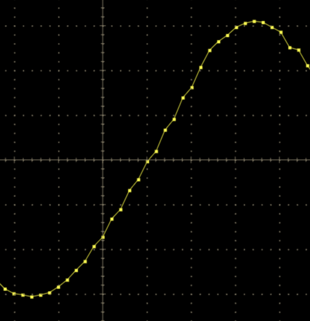 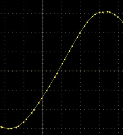
If your points do not lie on a smooth line, you might habe a problem such as the wrong channel for calibration, an offset of 1 in the index of the time array or some other software bug. Measure the same signal with the DRSOsc application and then your code. If the results differ, you have a software problem on your side.
Stefan
|
|
Tue Mar 15 13:07:50 2022, Matias Senger, Time calibration and the C++ API
|
Thanks for your help. If I look into the app the behavior for the 4 channels is exactly as you show:


Now, when I sample with my code something strange happens, two of the channels are fine and the other two are wrong:

This is a surprise to me because I acquire the 4 channels in the same way within a `for` loop. To get the time data I use `DRSBoard::GetTime` with the `tcalibrated` argument set to `true`. Is there any aditional step to use the calibration?
Best,
Matias.
| Stefan Ritt wrote: |
|
Looks like you have the some time calibration, not sure if it's the correct one. Sample the sine wave from the calibration clock, once with and once without the timing calibration, then you will see if all points lie on a smooth line. Left: without timing calibration, right: with proper timing calibration:
If your points do not lie on a smooth line, you might habe a problem such as the wrong channel for calibration, an offset of 1 in the index of the time array or some other software bug. Measure the same signal with the DRSOsc application and then your code. If the results differ, you have a software problem on your side.
Stefan
|
|
|
Sun Mar 6 17:54:47 2022, Matias Senger, Why does not trigger at higher sampling frequencies?
|
I have connected 3 signals to the DRS4 Evaluation Board V5 which look like this in the drsosc app:

Note that here I am sampling at 5 GS/s. Using this app everything works perfect.
Now I want to repeat this using the C++ API (which I am actually wrapping to use within Python, see here if interested https://github.com/SengerM/pydrs ) but can only make this to work at lower sampling frequencies up to 3.9 GS/s. This is how I am configuring the board followint the `drs_exam.cpp` file:
```python
board.set_sampling_frequency(Hz=SAMPLING_FREQ)
board.set_transparent_mode('on')
board.set_input_range(center=0)
board.enable_trigger(True,False) # Don't know what this line does, it was in the example `drs_exam.cpp`.
board.set_trigger_source('ch4')
board.set_trigger_level(volts=-.1)
board.set_trigger_polarity(edge='falling')
board.set_trigger_delay(seconds=TRIGGER_DELAY)
```
The full code is here https://github.com/SengerM/pydrs/blob/master/tests/test_drs.py but anyway, my previous snippet can be considered as pseudo-code and if more details needed I can provide.
This is what I get as I increase the sampling frequency:


Up to 3.95 GS/s it works perfectly. At >= 4 GS/s it just never triggers. A few times I was able to make this work at 4 and 5 GS/s playing with the trigger delay, but this seemed to be some kind of random luck because I was not able to replicate it even with the same values.
Any help is appreciated.
Best,
Matías. |
|
Mon Mar 7 08:45:32 2022, Stefan Ritt, Why does not trigger at higher sampling frequencies?
|
Unfortunately I have not idea what the problem could be. In principle the trigger should be independent of the sampling speed, since the trigger is only made with a discriminator and a flip-flop. The hardware must be ok since you see the trigger with the oscillocope app. All you can do is to go through the sorce code of the oscilloscope app, especially drsosc/Osic.cpp::ScanBoards(), SetTriggerLevel(), SetTriggerPolariy() etc. to make sure you do the same calls as the oscilloscope app.
Stefan |
|
Tue Mar 8 00:25:56 2022, Matias Senger, Why does not trigger at higher sampling frequencies?
|
I have seen in the app that the trigger source buttons do something different than the "or" and "transparent trigger" buttons:

If I enable the setup from the right, i.e. OR in CH4 and "Enable Transparent Trigger" the app stops triggering. This is the configuration that seems to be applied in the `drs_exam.cpp` code if I am not mistaken. For some reason in that code it still triggers (I have modified the code to trigger on CH4 instead of CH1 and the trigger level, polarity, etc.).
What does the button in the left actually do? The circular checkbox with the "4" I mean. This is the trigger configuration I want to get in the C++ code.
I also don't know what the function `DRSBoard::EnableTrigger` does, what is the meaning of `flag1` and `flag2`? In my code there is a call to this function which I copied from the example.
| Stefan Ritt wrote: |
|
Unfortunately I have not idea what the problem could be. In principle the trigger should be independent of the sampling speed, since the trigger is only made with a discriminator and a flip-flop. The hardware must be ok since you see the trigger with the oscillocope app. All you can do is to go through the sorce code of the oscilloscope app, especially drsosc/Osic.cpp::ScanBoards(), SetTriggerLevel(), SetTriggerPolariy() etc. to make sure you do the same calls as the oscilloscope app.
Stefan
|
|
|
Tue Mar 8 12:20:00 2022, Matias Senger, Why does not trigger at higher sampling frequencies?
|
Sorry for the spam. Just want to let you know that I was able to solve the problem, it was all due to a `float` being casted as `int` in the Python binding. Now it works like a charm.
| Matias Senger wrote: |
|
I have seen in the app that the trigger source buttons do something different than the "or" and "transparent trigger" buttons:
If I enable the setup from the right, i.e. OR in CH4 and "Enable Transparent Trigger" the app stops triggering. This is the configuration that seems to be applied in the `drs_exam.cpp` code if I am not mistaken. For some reason in that code it still triggers (I have modified the code to trigger on CH4 instead of CH1 and the trigger level, polarity, etc.).
What does the button in the left actually do? The circular checkbox with the "4" I mean. This is the trigger configuration I want to get in the C++ code.
I also don't know what the function `DRSBoard::EnableTrigger` does, what is the meaning of `flag1` and `flag2`? In my code there is a call to this function which I copied from the example.
| Stefan Ritt wrote: |
|
Unfortunately I have not idea what the problem could be. In principle the trigger should be independent of the sampling speed, since the trigger is only made with a discriminator and a flip-flop. The hardware must be ok since you see the trigger with the oscillocope app. All you can do is to go through the sorce code of the oscilloscope app, especially drsosc/Osic.cpp::ScanBoards(), SetTriggerLevel(), SetTriggerPolariy() etc. to make sure you do the same calls as the oscilloscope app.
Stefan
|
|
|
|
Tue Mar 1 19:03:37 2022, Keita Mizukoshi, Scaler issue to evaluate live time
|
Hi. I'm trying to evaluate livetime of the evaluation board with the hardware scaler. I'm facing a strange issue.
I took the rate with the function, DRS->GetScaler(int channel).
I guess that channels 0--3 mean the rate for the channel, and channel 4 means the counter of the trigger.
I took the 1,000 pulses generated by a pulse generator with 50 Hz.
The scaler values are ~ 39.83, not 50.
The timestamp difference between the initial event and the final event is 19.98 seconds.
1000/19.98 ~ 50, thus, the evaluation board took the pulses with enough livetime.
Can we believe the scaler value for the livetime evaluation? |
|
Thu Mar 3 16:14:16 2022, Stefan Ritt, Scaler issue to evaluate live time
|
The scalers are read out 10x per seconds, so they have an accuracy of 10 Hz. I tried a 50 Hz pulser, and measured 40 Hz, I tried 52 Hz and measured 50 Hz. This is about what you can expect.
The scaler rate is measured after the discriminator of the trigger, so the trigger level also affects the scaler reading. If you have a 100 mV pulse and your threshold is 200 mV, your scaler rate drops to zero. That can be seen best with the DRSOsc and sliding the trigger value. If you have a 50 Hz pulse with narrow (< us) pulses, things are fine. But if you use a 50 Hz square wave, then you get distorted signals due to the AC coupling which can also be confusing. See for example here: https://www.daqarta.com/dw_gg0o.htm
| Keita Mizukoshi wrote: |
|
Hi. I'm trying to evaluate livetime of the evaluation board with the hardware scaler. I'm facing a strange issue.
I took the rate with the function, DRS->GetScaler(int channel).
I guess that channels 0--3 mean the rate for the channel, and channel 4 means the counter of the trigger.
I took the 1,000 pulses generated by a pulse generator with 50 Hz.
The scaler values are ~ 39.83, not 50.
The timestamp difference between the initial event and the final event is 19.98 seconds.
1000/19.98 ~ 50, thus, the evaluation board took the pulses with enough livetime.
Can we believe the scaler value for the livetime evaluation?
|
|
|
Fri Mar 4 03:55:33 2022, Keita Mizukoshi, Scaler issue to evaluate live time
|
Thank you very much for your explanation.
I would like to show you a pulse example ('black line is the threshold).
Still, pulse generator rate and DRS4 rate are a bit different more than 10 Hz.
| Stefan Ritt wrote: |
|
The scalers are read out 10x per seconds, so they have an accuracy of 10 Hz. I tried a 50 Hz pulser, and measured 40 Hz, I tried 52 Hz and measured 50 Hz. This is about what you can expect.
The scaler rate is measured after the discriminator of the trigger, so the trigger level also affects the scaler reading. If you have a 100 mV pulse and your threshold is 200 mV, your scaler rate drops to zero. That can be seen best with the DRSOsc and sliding the trigger value. If you have a 50 Hz pulse with narrow (< us) pulses, things are fine. But if you use a 50 Hz square wave, then you get distorted signals due to the AC coupling which can also be confusing. See for example here: https://www.daqarta.com/dw_gg0o.htm
| Keita Mizukoshi wrote: |
|
Hi. I'm trying to evaluate livetime of the evaluation board with the hardware scaler. I'm facing a strange issue.
I took the rate with the function, DRS->GetScaler(int channel).
I guess that channels 0--3 mean the rate for the channel, and channel 4 means the counter of the trigger.
I took the 1,000 pulses generated by a pulse generator with 50 Hz.
The scaler values are ~ 39.83, not 50.
The timestamp difference between the initial event and the final event is 19.98 seconds.
1000/19.98 ~ 50, thus, the evaluation board took the pulses with enough livetime.
Can we believe the scaler value for the livetime evaluation?
|
|
|
|
Mon Mar 7 16:37:54 2022, Stefan Ritt, Scaler issue to evaluate live time
|
I tried your measurement with the DRSOscilloscope app (see below), and I measure a constant difference of 10 Hz among the whole range of 100 Hz to 3 kHz.
So I don't know what's wrong on your side. Did you try with the oscilloscope app as well? Have you checked your pulse generator? The evaluation board time reference is a quartz with an accuracy of 10^-5, so no way one can get there a difference you see.
Stefan
| Keita Mizukoshi wrote: |
|
Thank you very much for your explanation.
I would like to show you a pulse example ('black line is the threshold).
Still, pulse generator rate and DRS4 rate are a bit different more than 10 Hz.
| Stefan Ritt wrote: |
|
The scalers are read out 10x per seconds, so they have an accuracy of 10 Hz. I tried a 50 Hz pulser, and measured 40 Hz, I tried 52 Hz and measured 50 Hz. This is about what you can expect.
The scaler rate is measured after the discriminator of the trigger, so the trigger level also affects the scaler reading. If you have a 100 mV pulse and your threshold is 200 mV, your scaler rate drops to zero. That can be seen best with the DRSOsc and sliding the trigger value. If you have a 50 Hz pulse with narrow (< us) pulses, things are fine. But if you use a 50 Hz square wave, then you get distorted signals due to the AC coupling which can also be confusing. See for example here: https://www.daqarta.com/dw_gg0o.htm
| Keita Mizukoshi wrote: |
|
Hi. I'm trying to evaluate livetime of the evaluation board with the hardware scaler. I'm facing a strange issue.
I took the rate with the function, DRS->GetScaler(int channel).
I guess that channels 0--3 mean the rate for the channel, and channel 4 means the counter of the trigger.
I took the 1,000 pulses generated by a pulse generator with 50 Hz.
The scaler values are ~ 39.83, not 50.
The timestamp difference between the initial event and the final event is 19.98 seconds.
1000/19.98 ~ 50, thus, the evaluation board took the pulses with enough livetime.
Can we believe the scaler value for the livetime evaluation?
|
|
|
|
|
Mon Mar 7 13:38:03 2022, Radoslaw Marcinkowski, Problems with DRS4 Evaluation Board after Windows 10 upgrade - share of experiences
|
Dear DRS4 Users,
I would like to share my expireinces with using of DRS4 Evaluation Board software (oscilloscope) after upgrade of Windows 10.
I had Windows 10 (Enterprise) in version from ~2016. It was working fine with DRS4 Scope software. Due to the company policy, Windows was upgraded to the newer version (2019). Since this time the board was not recognized any more as DRS4 Evaluation Board, both by Windows and DRS4 Scope standard software. Changing USB sockets did not help at all. I installed once more time Zadig USB driver (suggested by https://www.psi.ch/en/drs/software-download), no Admistrator rights were needed. It took long time, about 10 minutes or more, it suggested restart in the meantime, and finally noticed that ... installation failed! Even that, DRS4 software started to recognize the board without the problem even without reboot. Let me notice that all users on this machine can use the DRS4 software even if installation was done by non-administrator user.
Regards,
Radek |
|
Wed Mar 2 17:25:10 2022, Matias Senger, How to convert samples to volt?
|
I am using the `drscl` app. My prior experience is practically zero, sorry if this is a very naive question. When I read using `read 0 1` (channel 0, with calibration) I get this:
```
Calibration not valid for board #2946
10 3 7 4 10 8 14 5 5 9 3 4 9 8 9 4
3 3 12 5 5 13 3 8 1 5 0 4 8 6 6 3
...etc...
```
Why does it says that the calibration is not valid? How am I supposed to go from integers to volts?
If I run the `info` command I get this:
```
==============================
Mezz. Board index: 0
DRS type: DRS4
Board type: 9
Serial number: 2946
Firmware revision: 30000
Temperature: 43.4 C
Input range: -0.5V...0.5V
Calibrated range: -0.5V...0.5V
Calibrated frequency: 0.000 GHz
Status reg.: 0000009A
Control reg.: 00000000
DMODE circular
Trigger bus: 00000000
Frequency: 1.007 GHz
``` |
|
Thu Mar 3 13:47:26 2022, Stefan Ritt, How to convert samples to volt?
|
The 'drscl' tool is more for experts, normal users are advised to use the DRSOsc oscilloscope.
The board has to be calibrated for a given sampling speed before calibrated data can be read out. Do that with the "calib" command, specifying 5 for the sampling rate, 0 for the range (which is the middle between -0.5 and +0.5) and 1 for 1024 mode. If you then do "start", "stop", "read 0 1" you get calibrated data in mV.
Stefan
| Matias Senger wrote: |
|
I am using the `drscl` app. My prior experience is practically zero, sorry if this is a very naive question. When I read using `read 0 1` (channel 0, with calibration) I get this:
```
Calibration not valid for board #2946
10 3 7 4 10 8 14 5 5 9 3 4 9 8 9 4
3 3 12 5 5 13 3 8 1 5 0 4 8 6 6 3
...etc...
```
Why does it says that the calibration is not valid? How am I supposed to go from integers to volts?
If I run the `info` command I get this:
```
==============================
Mezz. Board index: 0
DRS type: DRS4
Board type: 9
Serial number: 2946
Firmware revision: 30000
Temperature: 43.4 C
Input range: -0.5V...0.5V
Calibrated range: -0.5V...0.5V
Calibrated frequency: 0.000 GHz
Status reg.: 0000009A
Control reg.: 00000000
DMODE circular
Trigger bus: 00000000
Frequency: 1.007 GHz
```
|
|
|
Wed Feb 16 14:06:45 2022, Dmitry Hits, Sliders missing in drsosc
|
Hi everyone,
Did anyone have a "missing sliders problem" in GUI (see attachment) accompanied by the following message in the terminal.
(drsosc:4611): Gtk-WARNING **: 14:05:11.249: Negative content width -4 (allocation 20, extents 12x12) while allocating gadget (node scale, owner GtkScale)
(drsosc:4611): Gtk-WARNING **: 14:05:11.249: Negative content width -2 (allocation 0, extents 1x1) while allocating gadget (node trough, owner GtkScale)
If yes, how did you solve it?
All ideas are appreciated!
Cheers,
Dmitry
|
|
Sat Feb 12 13:06:56 2022, Matias Senger, Cannot trigger on pulses, have to trigger on undershoot
|
I am using the DRS4 board trying to measure pulses produced by an LGAD. I have no prior experience with this board, have just installed the `drsosc` application and am exploring. I am experiencing some strange trigger behavior. Consider the following screenshot:

Here nothing is strange, the board is triggering on the undershoot and it is working fine, I can trigger on rising/falling edge, different levels, etc.
Now, the strange thing is that if I pull the trigger up to trigger on the pulse itself it stops triggering:

I have tried many different setups for the trigger (rising, falling edge, different levels, etc) and nothing works. In the undershoot, everything works.
I have tried with the internal test signal and it works fine:

What could be the problem?
I have run the voltage and time calibrations as suggested in the manual. |
|
Tue Feb 15 12:02:29 2022, Stefan Ritt, Cannot trigger on pulses, have to trigger on undershoot
|
The trigger comparator is a ADCMP601 unit which requires a minimum pulse width of 3-4 ns. I see that your pulses are only 1-2 ns wide. You have to make your pulses wider in order to trigger on them.
Stefan |
|
Tue Feb 15 11:59:22 2022, Alex Myczko, apt install drs4eb
|
drs4b is now officially on these distributions:
https://repology.org/project/drs4eb/versions
enjoy |
|
Sat Jan 15 09:13:42 2022, student_riku, I want to know about the readout
|
Hello, everyone.
I'm a student in Japan.
Please forgive me if this is a very rudimentary question.
Am I right in thinking that inputting 1 to DMODE (Bit0) in the configuration register will connect the 1024th cell to the 1st cell?
Also, let's assume that after sampling 1024 cells on channel 0, 200 cells are sampled in the second week.
Does the readout of 1024 cells start from cell 0?
Or does it start from the 200th cell? |
|
Sat Jan 15 10:50:47 2022, Stefan Ritt, I want to know about the readout
|
| student_riku wrote: |
|
Am I right in thinking that inputting 1 to DMODE (Bit0) in the configuration register will connect the 1024th cell to the 1st cell?
|
Yes, as desceribed in the manual .
| student_riku wrote: |
|
Also, let's assume that after sampling 1024 cells on channel 0, 200 cells are sampled in the second week.
Does the readout of 1024 cells start from cell 0?
Or does it start from the 200th cell?
|
I don't understand what you mean by "second week".
Normally, you run the chip continously (DMODE=1) until you receive a trigger. Then, you typically read out the chip from the stop position by using a RSRLOAD pulse (as described unter "REGION-OF-INTEREST READOUT MODE".
Stefan |
|
Wed Jan 26 06:44:11 2022, student_riku, I want to know about the readout
|
Dear Stefan
Thanks a lot.
I solved it.
| Stefan Ritt wrote: |
| student_riku wrote: |
|
Am I right in thinking that inputting 1 to DMODE (Bit0) in the configuration register will connect the 1024th cell to the 1st cell?
|
Yes, as desceribed in the manual .
| student_riku wrote: |
|
Also, let's assume that after sampling 1024 cells on channel 0, 200 cells are sampled in the second week.
Does the readout of 1024 cells start from cell 0?
Or does it start from the 200th cell?
|
I don't understand what you mean by "second week".
Normally, you run the chip continously (DMODE=1) until you receive a trigger. Then, you typically read out the chip from the stop position by using a RSRLOAD pulse (as described unter "REGION-OF-INTEREST READOUT MODE".
Stefan
|
|
|
Tue Jan 25 14:15:00 2022, Thomas M., Regarding measuring for a set time
|
Hello,
I'm working on a project wherein we're looking at photomultipliers. We've already acquired a DRS4 evaluation board with the intent of using it to gather our data.
I've looked at the source code for the software with the intent of maybe writing a patch to add additional functionality. I was hoping you could answer some quick questions in that regard.
Am I correct in assuming that drsosc and drscl are functionally equivalent regarding collecting data? We want to run the DRS4-EB for a predefined amount of time. However, the DRS4 scope application seems only to run for a predefined set of measurements. Have I got that right? Is there some reason to avoid running the DRS4-EB for a predefined amount of time that I should be aware of?
Appreciate any help you can provide. Thanks!
Kind regards,
Thomas
|
|
Tue Jan 25 14:34:42 2022, Stefan Ritt, Regarding measuring for a set time
|
drsosc is a graphical application contiously acquiring data from the board, and drscl is a command line tool for debugging, as written in the manual.
The drsosc application runs indefinitely, but I guess you refer to saving data (by hitting the "Save" button in the drsosc application). Yes the save functionality has a number of events, since you cannot store data indefinitely, since your harddisk does not have indefinite space!
I kind of sense that you want to convert the "number of event to save" into "number of seconds or hours to save". This is not build into the drsosc application. It's all open source, so feel free to change the code. Alternatively, you can use the drs_exam.cpp program coming with the distribution, wich is a simpel C++ program reading the board. It has a for loop over 10 events, but you can change the code easily to run for a predetermined amount of time.
Stefan
| Thomas M. wrote: |
|
Am I correct in assuming that drsosc and drscl are functionally equivalent regarding collecting data? We want to run the DRS4-EB for a predefined amount of time. However, the DRS4 scope application seems only to run for a predefined set of measurements. Have I got that right? Is there some reason to avoid running the DRS4-EB for a predefined amount of time that I should be aware of?
|
|
|
Tue Jan 25 14:44:49 2022, Thomas M., Regarding measuring for a set time
|
Yes, you've got it exactly right. Thank you, that helps a lot!
Thomas
| Stefan Ritt wrote: |
|
drsosc is a graphical application contiously acquiring data from the board, and drscl is a command line tool for debugging, as written in the manual.
The drsosc application runs indefinitely, but I guess you refer to saving data (by hitting the "Save" button in the drsosc application). Yes the save functionality has a number of events, since you cannot store data indefinitely, since your harddisk does not have indefinite space!
I kind of sense that you want to convert the "number of event to save" into "number of seconds or hours to save". This is not build into the drsosc application. It's all open source, so feel free to change the code. Alternatively, you can use the drs_exam.cpp program coming with the distribution, wich is a simpel C++ program reading the board. It has a for loop over 10 events, but you can change the code easily to run for a predetermined amount of time.
Stefan
| Thomas M. wrote: |
|
Am I correct in assuming that drsosc and drscl are functionally equivalent regarding collecting data? We want to run the DRS4-EB for a predefined amount of time. However, the DRS4 scope application seems only to run for a predefined set of measurements. Have I got that right? Is there some reason to avoid running the DRS4-EB for a predefined amount of time that I should be aware of?
|
|
|
|
Thu Dec 23 03:42:26 2021, Lynsey, DRS4 request assistance
|
Dear Sir or Madam,
Good morning,I am using drs4 chip, and the measured fDTAP == 1/350ns, that is, fDOMINO == 1 / 350ns * 2048 == 5.8GHz.
I have three questions:
1. Is fDOMINO determined by the chip itself?
2. C1, C2 and R2 are TBD. I don't know how many to choose. Is there an algorithm?
3."Configure Write Shift Register to contain all 1's",What, pray, is the meaning of “1's"?
Truely yours.
|
|
Mon Jan 3 17:13:41 2022, Stefan Ritt, DRS4 request assistance
|
1. fDOMINO is defined as fREFCLK * 2048
2. Good values can be derived from the evaluation board schematics: C1=4.7nF, C2=1nF, R=130 Ohm
3. A "1" means a logical high level. See Wikipedia: https://en.wikipedia.org/wiki/Logic_level
| Lynsey wrote: |
|
Dear Sir or Madam,
Good morning,I am using drs4 chip, and the measured fDTAP == 1/350ns, that is, fDOMINO == 1 / 350ns * 2048 == 5.8GHz.
I have three questions:
1. Is fDOMINO determined by the chip itself?
2. C1, C2 and R2 are TBD. I don't know how many to choose. Is there an algorithm?
3."Configure Write Shift Register to contain all 1's",What, pray, is the meaning of “1's"?
Truely yours.
|
|
|
Fri Feb 26 17:05:26 2021, Tom Schneider, Trouble getting PLL to lock
|
Hello,
I am working on a custom PCB design with the DRS4 chip, and I can't get the PLL to lock. I'm feeding CLKIN with a 1MHz CMOS clock (REFCLK- tied to VDD/2), and I'm using the same loop filter as the eval board. I see from the datasheet that the PLL is enabled by default, so I'm not writing anything to the config register on startup. I am just driving DENABLE high approx. 100ms after startup and looking for the PLL lock bit to go high. When I look at DTAP, I see a 3MHz signal. Can anyone tell me what I'm doing wrong?
-Tom |
|
Fri Feb 26 17:59:14 2021, Stefan Ritt, Trouble getting PLL to lock
|
I guess you mean "1 MHz clock at REFCLK+", and not CLKIN, there is no CLKIN, just a SRCLK, but that is someting else!
There could be many reasons why this is not working. It's hard for me to debug your board without actually having it in hands. So just some ideas:
- Supply a clean differential REFCLK, I never tried one end tied to VDD/2
- Is /RESET high?
- Is BIAS at roughly 0.7V?
- Is A0-A3 different from 1111, which puts the chip in standby
- Did you double check your loop filter?
The easiest usually is to start from a running evaluation board, then compare all pins 1:1 with your board.
Stefan
| Tom Schneider wrote: |
|
Hello,
I am working on a custom PCB design with the DRS4 chip, and I can't get the PLL to lock. I'm feeding CLKIN with a 1MHz CMOS clock (REFCLK- tied to VDD/2), and I'm using the same loop filter as the eval board. I see from the datasheet that the PLL is enabled by default, so I'm not writing anything to the config register on startup. I am just driving DENABLE high approx. 100ms after startup and looking for the PLL lock bit to go high. When I look at DTAP, I see a 3MHz signal. Can anyone tell me what I'm doing wrong?
-Tom
|
|
|
Fri Feb 26 18:33:52 2021, Tom Schneider, Trouble getting PLL to lock
|
Stefan,
Thanks for responding so quickly. Yes I have my clock source going to REFCLK+ (CLKIN is the signal name on my schematic). BIAS is 0.7V exactly, /RESET is high, A0-A3 are 0x0000, and the loop filter has a 4.7nF cap to GND with a 130ohm resistor + 1uF cap in parallel, just like the eval board.
Regarding the clock - I am not using an LVDS clock, but rather a 2.5V-level clock signal, with REFCLK- tied to 1.25V. Sheet 9 of the datasheet states: If no LVDS reference clock signal is available, a CMOS signal can be connected to REFCLK+ and the REFCLK input is connected to VDD/2 via a resistor divider.
Is that not a true statement?
-Tom
| Stefan Ritt wrote: |
|
I guess you mean "1 MHz clock at REFCLK+", and not CLKIN, there is no CLKIN, just a SRCLK, but that is someting else!
There could be many reasons why this is not working. It's hard for me to debug your board without actually having it in hands. So just some ideas:
- Supply a clean differential REFCLK, I never tried one end tied to VDD/2
- Is /RESET high?
- Is BIAS at roughly 0.7V?
- Is A0-A3 different from 1111, which puts the chip in standby
- Did you double check your loop filter?
The easiest usually is to start from a running evaluation board, then compare all pins 1:1 with your board.
Stefan
| Tom Schneider wrote: |
|
Hello,
I am working on a custom PCB design with the DRS4 chip, and I can't get the PLL to lock. I'm feeding CLKIN with a 1MHz CMOS clock (REFCLK- tied to VDD/2), and I'm using the same loop filter as the eval board. I see from the datasheet that the PLL is enabled by default, so I'm not writing anything to the config register on startup. I am just driving DENABLE high approx. 100ms after startup and looking for the PLL lock bit to go high. When I look at DTAP, I see a 3MHz signal. Can anyone tell me what I'm doing wrong?
-Tom
|
|
|
|
Fri Feb 26 20:32:25 2021, Stefan Ritt, Trouble getting PLL to lock
|
Can you post a scope trace of your refclk together with DTAP, DSPEED and DENABLE?
| Tom Schneider wrote: |
|
Stefan,
Thanks for responding so quickly. Yes I have my clock source going to REFCLK+ (CLKIN is the signal name on my schematic). BIAS is 0.7V exactly, /RESET is high, A0-A3 are 0x0000, and the loop filter has a 4.7nF cap to GND with a 130ohm resistor + 1uF cap in parallel, just like the eval board.
Regarding the clock - I am not using an LVDS clock, but rather a 2.5V-level clock signal, with REFCLK- tied to 1.25V. Sheet 9 of the datasheet states: If no LVDS reference clock signal is available, a CMOS signal can be connected to REFCLK+ and the REFCLK input is connected to VDD/2 via a resistor divider.
Is that not a true statement?
-Tom
| Stefan Ritt wrote: |
|
I guess you mean "1 MHz clock at REFCLK+", and not CLKIN, there is no CLKIN, just a SRCLK, but that is someting else!
There could be many reasons why this is not working. It's hard for me to debug your board without actually having it in hands. So just some ideas:
- Supply a clean differential REFCLK, I never tried one end tied to VDD/2
- Is /RESET high?
- Is BIAS at roughly 0.7V?
- Is A0-A3 different from 1111, which puts the chip in standby
- Did you double check your loop filter?
The easiest usually is to start from a running evaluation board, then compare all pins 1:1 with your board.
Stefan
| Tom Schneider wrote: |
|
Hello,
I am working on a custom PCB design with the DRS4 chip, and I can't get the PLL to lock. I'm feeding CLKIN with a 1MHz CMOS clock (REFCLK- tied to VDD/2), and I'm using the same loop filter as the eval board. I see from the datasheet that the PLL is enabled by default, so I'm not writing anything to the config register on startup. I am just driving DENABLE high approx. 100ms after startup and looking for the PLL lock bit to go high. When I look at DTAP, I see a 3MHz signal. Can anyone tell me what I'm doing wrong?
-Tom
|
|
|
|
|
Fri Feb 26 21:24:39 2021, Tom Schneider, Trouble getting PLL to lock
|
Probe capacitance makes that tricky - if I put my probe on DSPEED, I see that it starts at approx. 2.5V then gradually decreases until it hits 0V. DTAP decreases from 3MHz to 0 during this time.
I'll try to get something together to show you.
| Stefan Ritt wrote: |
|
Can you post a scope trace of your refclk together with DTAP, DSPEED and DENABLE?
| Tom Schneider wrote: |
|
Stefan,
Thanks for responding so quickly. Yes I have my clock source going to REFCLK+ (CLKIN is the signal name on my schematic). BIAS is 0.7V exactly, /RESET is high, A0-A3 are 0x0000, and the loop filter has a 4.7nF cap to GND with a 130ohm resistor + 1uF cap in parallel, just like the eval board.
Regarding the clock - I am not using an LVDS clock, but rather a 2.5V-level clock signal, with REFCLK- tied to 1.25V. Sheet 9 of the datasheet states: If no LVDS reference clock signal is available, a CMOS signal can be connected to REFCLK+ and the REFCLK input is connected to VDD/2 via a resistor divider.
Is that not a true statement?
-Tom
| Stefan Ritt wrote: |
|
I guess you mean "1 MHz clock at REFCLK+", and not CLKIN, there is no CLKIN, just a SRCLK, but that is someting else!
There could be many reasons why this is not working. It's hard for me to debug your board without actually having it in hands. So just some ideas:
- Supply a clean differential REFCLK, I never tried one end tied to VDD/2
- Is /RESET high?
- Is BIAS at roughly 0.7V?
- Is A0-A3 different from 1111, which puts the chip in standby
- Did you double check your loop filter?
The easiest usually is to start from a running evaluation board, then compare all pins 1:1 with your board.
Stefan
| Tom Schneider wrote: |
|
Hello,
I am working on a custom PCB design with the DRS4 chip, and I can't get the PLL to lock. I'm feeding CLKIN with a 1MHz CMOS clock (REFCLK- tied to VDD/2), and I'm using the same loop filter as the eval board. I see from the datasheet that the PLL is enabled by default, so I'm not writing anything to the config register on startup. I am just driving DENABLE high approx. 100ms after startup and looking for the PLL lock bit to go high. When I look at DTAP, I see a 3MHz signal. Can anyone tell me what I'm doing wrong?
-Tom
|
|
|
|
|
|
Fri Feb 26 22:12:58 2021, Stefan Ritt, Trouble getting PLL to lock
|
Sounds to me like your REFCLK is not getting through or your PLL loop is open. Could be a bad solder connection. Try to measure signals not on the PCB trace, but directly on the DRS4 pins. Drive REFCLK with a proper LVDS signal. Maybe it's wrong what I wrote in the data sheet and the trick with VDD/2 is not really working.
Stefan |
|
Fri Feb 26 22:52:13 2021, Tom Schneider, Trouble getting PLL to lock
|
Thats not a simple modification to my PCB, but I'll give it a try. Thanks for your help
| Stefan Ritt wrote: |
|
Sounds to me like your REFCLK is not getting through or your PLL loop is open. Could be a bad solder connection. Try to measure signals not on the PCB trace, but directly on the DRS4 pins. Drive REFCLK with a proper LVDS signal. Maybe it's wrong what I wrote in the data sheet and the trick with VDD/2 is not really working.
Stefan
|
|
|
Thu Mar 4 21:36:14 2021, Tom Schneider, Trouble getting PLL to lock
|
I found the problem, and it had nothing to do with the CMOS clock input. As it turns out, even though I was using the default state of the config register, I still had to write to it after powerup. Once I did that, the PLL locked immediately.
-Tom
| Tom Schneider wrote: |
|
Thats not a simple modification to my PCB, but I'll give it a try. Thanks for your help
| Stefan Ritt wrote: |
|
Sounds to me like your REFCLK is not getting through or your PLL loop is open. Could be a bad solder connection. Try to measure signals not on the PCB trace, but directly on the DRS4 pins. Drive REFCLK with a proper LVDS signal. Maybe it's wrong what I wrote in the data sheet and the trick with VDD/2 is not really working.
Stefan
|
|
|
|
Fri Mar 5 09:39:42 2021, Stefan Ritt, Trouble getting PLL to lock
|
That probably depends on the way your FPGA boots. If the SRCLK signal goes high after the SRIN - even a few ns - you might clock one or two zeros into the config register, thus disabling the PLL. Shame that I haven't thought of this before.
Stefan |
|
Fri Dec 24 03:13:32 2021, Lynsey, Trouble getting PLL to lock
|
I also design the circuit myself. Our problem is the same. Can we communicate?
| Stefan Ritt wrote: |
|
I guess you mean "1 MHz clock at REFCLK+", and not CLKIN, there is no CLKIN, just a SRCLK, but that is someting else!
There could be many reasons why this is not working. It's hard for me to debug your board without actually having it in hands. So just some ideas:
- Supply a clean differential REFCLK, I never tried one end tied to VDD/2
- Is /RESET high?
- Is BIAS at roughly 0.7V?
- Is A0-A3 different from 1111, which puts the chip in standby
- Did you double check your loop filter?
The easiest usually is to start from a running evaluation board, then compare all pins 1:1 with your board.
Stefan
| Tom Schneider wrote: |
|
Hello,
I am working on a custom PCB design with the DRS4 chip, and I can't get the PLL to lock. I'm feeding CLKIN with a 1MHz CMOS clock (REFCLK- tied to VDD/2), and I'm using the same loop filter as the eval board. I see from the datasheet that the PLL is enabled by default, so I'm not writing anything to the config register on startup. I am just driving DENABLE high approx. 100ms after startup and looking for the PLL lock bit to go high. When I look at DTAP, I see a 3MHz signal. Can anyone tell me what I'm doing wrong?
-Tom
|
|
|
|
Tue Nov 16 01:27:51 2021, Jacquelynne Vaughan, V3 board, only one channel works, all components at each channel input working
|
Hi everyone,
I'm still looking through the forum for an answer to this question, but thought I'd go ahead and post anyway just in case it hasn't been answered yet. If it has I can take this post down.
I have a V3 board, and as far as I can tell only channel 2 gives an output. If I enable other channels using the DRS Oscilloscope software, they do show static but will not show a signal if I connect one to them (e.g. a series of subsequent square waves). A technician and I took the board out and tested all the components leading up to the microcontrollers for each channel, and everything seemed to be working fine. I thought maybe it was configured to only have one channel read an output, but I looked through the Config panel in the software and nothing seemed to indicate that.
I am a novice, and maybe I'm missing something that I didn't see in the manual. I can post screenshots if needed!
Thank you for your help! |
|
Tue Nov 16 08:51:14 2021, Stefan Ritt, V3 board, only one channel works, all components at each channel input working
|
A V3 boards is already 10 years old and out of warranty. The software has no configuration to turn channels off except the channel buttons on the main page on top of the sliders. I presume the channels are broked due to some overvoltage applied to them (the V5 board is better protected against over voltage). You can send it the board for repair, but it will cost almost the same amount of money than buying a new boards.
Regards,
Stefan
| Jacquelynne Vaughan wrote: |
|
Hi everyone,
I'm still looking through the forum for an answer to this question, but thought I'd go ahead and post anyway just in case it hasn't been answered yet. If it has I can take this post down.
I have a V3 board, and as far as I can tell only channel 2 gives an output. If I enable other channels using the DRS Oscilloscope software, they do show static but will not show a signal if I connect one to them (e.g. a series of subsequent square waves). A technician and I took the board out and tested all the components leading up to the microcontrollers for each channel, and everything seemed to be working fine. I thought maybe it was configured to only have one channel read an output, but I looked through the Config panel in the software and nothing seemed to indicate that.
I am a novice, and maybe I'm missing something that I didn't see in the manual. I can post screenshots if needed!
Thank you for your help!
|
|
|
Mon Sep 6 14:42:23 2021, Jiaolong, how to acquire the stop channel with 2x4096 cascading
|
Hi Steffan,
I have a question about how to acquire the stop channel:
Process: Configure the Write Shift Register with 00010001b to achieve 4-channel cascading, then after a trigger, set A3-A0 to 1101, sclk keeps 0.
Result: the WSROUT pin keeps 0, the SROUT pin has no clock pulse as written in datasheet, but keeps always 1 or 0. It can be seen the stop channel is channel 0 or channel 1, but no situation to represtent channel 3 or channel 4. And if set sclk with 8 pulses, the WSROUT and SROUT both keep 0.
What should I pay attention to? Looking forward to your reply.
Jiaolong |
|
Sat Sep 18 15:47:50 2021, Stefan Ritt, how to acquire the stop channel with 2x4096 cascading
|
The problem must be on your side, since the Write Shift Register readout works in other applications with the DRS4 chip. So I can only speculate what could be wrong:
- Do you really properly set the WSR? When you program it with 00010001b, add 8 more clock cycles and you should see the 00010001b pattern at WSROUT.
- Do all tests with an oscilloscope, to avoid potential problems in your FPGA firmware (like an input configures as an output by mistake).
- DWRITE must be high to see the contents of the WSR at the WSROUT pin, maybe that’s your mistake, see datasheet p 5 of 16.
- To see the contents of the WSR at SROUT, A0-3 must be 1101b, please check with your oscilloscope
- The addresses A0-A3 are simply connected to a multiplexer, so no clock is necessary after the addresses change
Stefan
| Jiaolong wrote: |
|
Hi Steffan,
I have a question about how to acquire the stop channel:
Process: Configure the Write Shift Register with 00010001b to achieve 4-channel cascading, then after a trigger, set A3-A0 to 1101, sclk keeps 0.
Result: the WSROUT pin keeps 0, the SROUT pin has no clock pulse as written in datasheet, but keeps always 1 or 0. It can be seen the stop channel is channel 0 or channel 1, but no situation to represtent channel 3 or channel 4. And if set sclk with 8 pulses, the WSROUT and SROUT both keep 0.
What should I pay attention to? Looking forward to your reply.
Jiaolong
|
|
|
Fri Nov 5 01:12:10 2021, Jiaolong, how to acquire the stop channel with 2x4096 cascading
|
Thanks for your advice. The problem has been solved by setting the srin again while reading out from srout.
| Stefan Ritt wrote: |
|
The problem must be on your side, since the Write Shift Register readout works in other applications with the DRS4 chip. So I can only speculate what could be wrong:
- Do you really properly set the WSR? When you program it with 00010001b, add 8 more clock cycles and you should see the 00010001b pattern at WSROUT.
- Do all tests with an oscilloscope, to avoid potential problems in your FPGA firmware (like an input configures as an output by mistake).
- DWRITE must be high to see the contents of the WSR at the WSROUT pin, maybe that’s your mistake, see datasheet p 5 of 16.
- To see the contents of the WSR at SROUT, A0-3 must be 1101b, please check with your oscilloscope
- The addresses A0-A3 are simply connected to a multiplexer, so no clock is necessary after the addresses change
Stefan
| Jiaolong wrote: |
|
Hi Steffan,
I have a question about how to acquire the stop channel:
Process: Configure the Write Shift Register with 00010001b to achieve 4-channel cascading, then after a trigger, set A3-A0 to 1101, sclk keeps 0.
Result: the WSROUT pin keeps 0, the SROUT pin has no clock pulse as written in datasheet, but keeps always 1 or 0. It can be seen the stop channel is channel 0 or channel 1, but no situation to represtent channel 3 or channel 4. And if set sclk with 8 pulses, the WSROUT and SROUT both keep 0.
What should I pay attention to? Looking forward to your reply.
Jiaolong
|
|
|
|
Mon Oct 25 18:48:04 2021, Javier Caravaca, Trigger multiple boards independently
|
Hello,
I recently acquired 4 DRS4 boards and I wanted to ask if it was possible to trigger them independently from the same computer.
I know that you can daisy-chain boards and trigger them all at the same time, but in my case, each of my boards record independent events, so I want them to trigger when trigger conditions are met in each board. I currently use the provided DRSOSC software, that can trigger on only the board that is being displayed at that moment. I tried opening several instances of DRSOSC to associate each to each board, but that is not possible since the second instance already does not find the boards. I wonder if there is a way of triggering from each board independently without having to use four computers.
Thank you,
Javier. |
|
Tue Oct 26 12:02:56 2021, Stefan Ritt, Trigger multiple boards independently
|
Unfortunately an independent operation from a single computer is not supported by the software. You can try to modify the drs_exam program and extend it. You can poll all boards in sequence and just read out that one which got a trigger, then start the loop again. But I don't know how good you are in programming. I needs a bit of experience to do that.
Stefan
| Javier Caravaca wrote: |
|
Hello,
I recently acquired 4 DRS4 boards and I wanted to ask if it was possible to trigger them independently from the same computer.
I know that you can daisy-chain boards and trigger them all at the same time, but in my case, each of my boards record independent events, so I want them to trigger when trigger conditions are met in each board. I currently use the provided DRSOSC software, that can trigger on only the board that is being displayed at that moment. I tried opening several instances of DRSOSC to associate each to each board, but that is not possible since the second instance already does not find the boards. I wonder if there is a way of triggering from each board independently without having to use four computers.
Thank you,
Javier.
|
|
|
Tue Oct 26 23:18:32 2021, Javier Caravaca, Trigger multiple boards independently
|
Thank you Stefan. Actually I noticed that the source code of drs_exam was available after I started this thread, and that was the solution that occurred to me too. I'll give that a try.
A related question is: if the 4 boards are triggering at max rate (500Hz), would the total data throughtput (of the four boards together) be 2GHz (500Hz x 4)? Or is the limitation on the readout, rather than the triggering?
Best,
Javier.
| Stefan Ritt wrote: |
|
Unfortunately an independent operation from a single computer is not supported by the software. You can try to modify the drs_exam program and extend it. You can poll all boards in sequence and just read out that one which got a trigger, then start the loop again. But I don't know how good you are in programming. I needs a bit of experience to do that.
Stefan
| Javier Caravaca wrote: |
|
Hello,
I recently acquired 4 DRS4 boards and I wanted to ask if it was possible to trigger them independently from the same computer.
I know that you can daisy-chain boards and trigger them all at the same time, but in my case, each of my boards record independent events, so I want them to trigger when trigger conditions are met in each board. I currently use the provided DRSOSC software, that can trigger on only the board that is being displayed at that moment. I tried opening several instances of DRSOSC to associate each to each board, but that is not possible since the second instance already does not find the boards. I wonder if there is a way of triggering from each board independently without having to use four computers.
Thank you,
Javier.
|
|
|
|
Wed Oct 27 08:11:42 2021, Stefan Ritt, Trigger multiple boards independently
|
I'm not sure if the rate would go up to 2 kHz (not 2 GHz!). Depends how the USB hub is designed. What you can do however is to buy 4 RaspberryPis (total cost 150$) and run everythign in parallel. The evaluation boards works nicely with the Pi's.
| Javier Caravaca wrote: |
|
A related question is: if the 4 boards are triggering at max rate (500Hz), would the total data throughtput (of the four boards together) be 2GHz (500Hz x 4)? Or is the limitation on the readout, rather than the triggering?
|
|
|
Tue Oct 26 10:41:46 2021, Mehrpad Monajem, External trigger and drs_exam
|
Hi Stefan,
I have two problems regarding using the drs_exam file with external trigger:
1- I connected a 200Khz signal with 20ns rising edge, 50 ohm load, and 27% duty cycle as an external trigger. The output of the drs_exam file starts from 0 to 200ns. Since I use an external trigger, I think it should be starting from 0 to 5ns and then again starting from 0. Could you please tell me where the problem is?
2- How is it possible to change from 1024 to 2048 bins in the drs_exam example?
You can find my code in the attachment.
Best regards,
Mehrpad |
|
Tue Oct 26 12:00:51 2021, Stefan Ritt, External trigger and drs_exam
|
1. Why should your waveform start from 0 to 5ns? I don't get your point. Whenever you trigger a readout, you get a 200ns wide time window, and by definition it starts at zero.
2. In the software distribution you have a drs_exam_2048.cpp program. Note that your board needs to be physically modified before delivery to switch to 2048 bins.
Best,
Stefan
| Mehrpad Monajem wrote: |
|
Hi Stefan,
I have two problems regarding using the drs_exam file with external trigger:
1- I connected a 200Khz signal with 20ns rising edge, 50 ohm load, and 27% duty cycle as an external trigger. The output of the drs_exam file starts from 0 to 200ns. Since I use an external trigger, I think it should be starting from 0 to 5ns and then again starting from 0. Could you please tell me where the problem is?
2- How is it possible to change from 1024 to 2048 bins in the drs_exam example?
You can find my code in the attachment.
Best regards,
Mehrpad
|
|
|
Tue Oct 26 15:05:18 2021, Mehrpad Monajem, External trigger and drs_exam
|
Thanks for your reply.
1- I want to have a window size of 25.6ns instead of 200ns at 5GSPS. I have a 200khz high voltage pulser, which applies a pulse to my sample. I want to digitize the detector signal for each pulse (each pulse has a 25.6ns period). The pulser and digitizer use same 200khz trigger signal from each channel of the signal generator.
2- My DRS board has a 2048 combined stick on it. But the software distribution that I have doesn't contain the drs_exam_2048.cpp program. Could you please send the link that I can download this program? I can't find it under the link below.
link: https://www.dropbox.com/sh/clqo7ekr0ysbrip/AACoWJzrQAbf3WiBJHG89bGGa?dl=0
Best regards,
Mehrpad
| Stefan Ritt wrote: |
|
1. Why should your waveform start from 0 to 5ns? I don't get your point. Whenever you trigger a readout, you get a 200ns wide time window, and by definition it starts at zero.
2. In the software distribution you have a drs_exam_2048.cpp program. Note that your board needs to be physically modified before delivery to switch to 2048 bins.
Best,
Stefan
| Mehrpad Monajem wrote: |
|
Hi Stefan,
I have two problems regarding using the drs_exam file with external trigger:
1- I connected a 200Khz signal with 20ns rising edge, 50 ohm load, and 27% duty cycle as an external trigger. The output of the drs_exam file starts from 0 to 200ns. Since I use an external trigger, I think it should be starting from 0 to 5ns and then again starting from 0. Could you please tell me where the problem is?
2- How is it possible to change from 1024 to 2048 bins in the drs_exam example?
You can find my code in the attachment.
Best regards,
Mehrpad
|
|
|
|
Thu Oct 14 15:19:00 2021, Keita Mizukoshi, livetime (or deadtime) of DRS4 evaluation board
|
Dear experts,
I would like to use the DRS4 evaluation board for actual physics experiment.
I made a CUI script based on the drs_exam, https://github.com/mzks/drs4_tools/blob/main/build/source/drscmd.cpp.
In this framework, how can we obtain DAQ livetime (or deadtime)?
Has some function already provided to evaluate them from firmware?
Best regards,
Keita |
|
Thu Oct 14 15:25:07 2021, Stefan Ritt, livetime (or deadtime) of DRS4 evaluation board
|
The one thing you can do easily is to look at the scaler values. If one channel counts all physical events, and you have all read out events, then the ratio give you the live/deadtime. The hardware scalers also keep running during the DRS readout.
Stefan
| Keita Mizukoshi wrote: |
|
Dear experts,
I would like to use the DRS4 evaluation board for actual physics experiment.
I made a CUI script based on the drs_exam, https://github.com/mzks/drs4_tools/blob/main/build/source/drscmd.cpp.
In this framework, how can we obtain DAQ livetime (or deadtime)?
Has some function already provided to evaluate them from firmware?
Best regards,
Keita
|
|
|
Thu Oct 14 18:03:52 2021, Keita Mizukoshi, livetime (or deadtime) of DRS4 evaluation board
|
Thank you very much for your response.
Excuse me for my very stupid confirmation.
If I take N events finally and the hardware scaler value is M, the livetime is realtime*(N/M). Is this correct?
| Stefan Ritt wrote: |
|
The one thing you can do easily is to look at the scaler values. If one channel counts all physical events, and you have all read out events, then the ratio give you the live/deadtime. The hardware scalers also keep running during the DRS readout.
Stefan
| Keita Mizukoshi wrote: |
|
Dear experts,
I would like to use the DRS4 evaluation board for actual physics experiment.
I made a CUI script based on the drs_exam, https://github.com/mzks/drs4_tools/blob/main/build/source/drscmd.cpp.
In this framework, how can we obtain DAQ livetime (or deadtime)?
Has some function already provided to evaluate them from firmware?
Best regards,
Keita
|
|
|
|
Thu Oct 14 18:42:31 2021, Stefan Ritt, livetime (or deadtime) of DRS4 evaluation board
|
I would say not exactly, but it's a good approximation.
| Keita Mizukoshi wrote: |
|
Thank you very much for your response.
Excuse me for my very stupid confirmation.
If I take N events finally and the hardware scaler value is M, the livetime is realtime*(N/M). Is this correct
|
|
|
Fri Oct 15 06:15:53 2021, Keita Mizukoshi, livetime (or deadtime) of DRS4 evaluation board
|
Thank you very much.
| Stefan Ritt wrote: |
|
I would say not exactly, but it's a good approximation.
| Keita Mizukoshi wrote: |
|
Thank you very much for your response.
Excuse me for my very stupid confirmation.
If I take N events finally and the hardware scaler value is M, the livetime is realtime*(N/M). Is this correct
|
|
|
|
Thu Sep 16 19:04:06 2021, Patrick Moriishi Freeman, drs_exam_multi with non-v4 boards, default configuration
|
Hello,
I made a modified version drs_exam_multi.cpp, but ran into an issue when running. When I ran it, it only found the two boards with lower serial numbers (2781 and 2879) and complained that the others (2880 and 2881) were not v4. Would there be a simple workaround for this type of thing? Also, would I be able to use the .dat format to keep the file sizes down.
If not, I am curious if there is a way I can at least set a default configuration for the drsosc program. It seems the drsosc.cfg is written when drsosc starts? Does it load the configuration from somewhere else? It would be very helpful to keep the same settings between runs, in particular the trigger delays, levels, trigger mode, and voltage offsets. Maybe I can even do this with just a few of the CLI commands? I know this is for experts only, but I think I would just need a few commands (setTrig, setTrigMode, setTrigDelay, that sort of thing) if they do exist. I would check the help now, but I'm running, and I'm pretty sure I saw some for trigger settings.
Anyhow, any help is appreciated in creating a more repeatable and automated data acquisition. Thanks!
|
|
Sat Sep 18 15:48:30 2021, Stefan Ritt, drs_exam_multi with non-v4 boards, default configuration
|
Hi,
please note the the evaluation board is what it says, a board to evaluate the chip, and is not meant for a full-blown shiny multi-board DAQ channel, so support for that is kind of limited.
Strange that you only find two out of four boards. What happens if you disconnect the two boards the system finds and then try again? Might be that your USB hub does not have enough power to supply four boards (each taking 2.5W, so you need 10W in total). Unplugging some board will show you if you have a power problem.
The drsosc.cfg stores the current configuration. For this to work, the drsosc program has to have write access to the directory where the drsosc.cfg program is stored, which is usually the directory from where the program is started. Maybe you have to adjust permissions. Yes you have commands to set everything, just look into drs_exam.cpp and you will find most of them.
Best,
Stefan
| Patrick Moriishi Freeman wrote: |
|
Hello,
I made a modified version drs_exam_multi.cpp, but ran into an issue when running. When I ran it, it only found the two boards with lower serial numbers (2781 and 2879) and complained that the others (2880 and 2881) were not v4. Would there be a simple workaround for this type of thing? Also, would I be able to use the .dat format to keep the file sizes down.
If not, I am curious if there is a way I can at least set a default configuration for the drsosc program. It seems the drsosc.cfg is written when drsosc starts? Does it load the configuration from somewhere else? It would be very helpful to keep the same settings between runs, in particular the trigger delays, levels, trigger mode, and voltage offsets. Maybe I can even do this with just a few of the CLI commands? I know this is for experts only, but I think I would just need a few commands (setTrig, setTrigMode, setTrigDelay, that sort of thing) if they do exist. I would check the help now, but I'm running, and I'm pretty sure I saw some for trigger settings.
Anyhow, any help is appreciated in creating a more repeatable and automated data acquisition. Thanks!
|
|
|
Wed Jul 14 14:55:09 2021, Mehrpad Monajem, C code to read the 4 channel with external trigger
|
Hi there,
Recently I bought a 5GSPS evaluation board with 2048 sampling points.
I want to read 4 inputs of the evaluation bord ar 5 GSPS or 2.5GSP and use an external trigger.
I've checked your website and download drs-5.0.5 which contains the source code in C. It seems that the file drs_exam.cpp can do what I am looking for.
So far I could make and compile the project in Linux Ubuntu, but I couldn't compile it in Windows 10. I've used Cygwin64 to compile the project in windows 10.
I have the following questions:
1- Since I only need to compile the drs_exam.cpp file, could please help me with how can I compile it directly(without making the entire project). Or tell me which version of Wxwidget and libusb I have to install.
2- If you have any sample code that can read 4 inputs with an external trigger, please tell me where can I find it.
In the end, I want to write a wrapper on this C file(which returns digitized data) and run it from my python program. Thank you in advance.
Best regards,
Mehrpad
|
|
Mon Aug 9 12:50:31 2021, Stefan Ritt, C code to read the 4 channel with external trigger
|
Sorry the late reply, I was on vacation.
Here are some answers:
1. I'm sorry I can't help much here, since I currently don't have a Windows 10 computer here to compile any code. I moved now completely to MacOSX, being very similar to Linux. I'm not allowed to run a Windows 7 computer any more for security reasons. Last time this worked for me was with Wxwidget version 3.0 and libusb 1.0, but I guess libusb is not critical so you can use a newer version. If you just compile drs_exam.cpp, you don't need any Wxwidget library. That one is only used for the oscilloscope program.
2. The program drs_exam_2048.cpp is meant to read channels in 2048-bin mode.
3. To adjust the delay between the trigger and the readout, use the function b->SetTriggerDelayNs(xxx)
Best,
Stefan
| Mehrpad Monajem wrote: |
|
Hi there,
Recently I bought a 5GSPS evaluation board with 2048 sampling points.
I want to read 4 inputs of the evaluation bord ar 5 GSPS or 2.5GSP and use an external trigger.
I've checked your website and download drs-5.0.5 which contains the source code in C. It seems that the file drs_exam.cpp can do what I am looking for.
So far I could make and compile the project in Linux Ubuntu, but I couldn't compile it in Windows 10. I've used Cygwin64 to compile the project in windows 10.
I have the following questions:
1- Since I only need to compile the drs_exam.cpp file, could please help me with how can I compile it directly(without making the entire project). Or tell me which version of Wxwidget and libusb I have to install.
2- If you have any sample code that can read 4 inputs with an external trigger, please tell me where can I find it.
In the end, I want to write a wrapper on this C file(which returns digitized data) and run it from my python program. Thank you in advance.
Best regards,
Mehrpad
|
|
|
Tue Aug 10 13:57:09 2021, Mehrpad Monajem, C code to read the 4 channel with external trigger
|
Thank you for the reply.
In the version that I have, I cannot find drs_exam_2048.cpp file. Could you please send me the link to download the software folder, which contain this file.
Best,
Mehrpad
| Stefan Ritt wrote: |
|
Sorry the late reply, I was on vacation.
Here are some answers:
1. I'm sorry I can't help much here, since I currently don't have a Windows 10 computer here to compile any code. I moved now completely to MacOSX, being very similar to Linux. I'm not allowed to run a Windows 7 computer any more for security reasons. Last time this worked for me was with Wxwidget version 3.0 and libusb 1.0, but I guess libusb is not critical so you can use a newer version. If you just compile drs_exam.cpp, you don't need any Wxwidget library. That one is only used for the oscilloscope program.
2. The program drs_exam_2048.cpp is meant to read channels in 2048-bin mode.
3. To adjust the delay between the trigger and the readout, use the function b->SetTriggerDelayNs(xxx)
Best,
Stefan
| Mehrpad Monajem wrote: |
|
Hi there,
Recently I bought a 5GSPS evaluation board with 2048 sampling points.
I want to read 4 inputs of the evaluation bord ar 5 GSPS or 2.5GSP and use an external trigger.
I've checked your website and download drs-5.0.5 which contains the source code in C. It seems that the file drs_exam.cpp can do what I am looking for.
So far I could make and compile the project in Linux Ubuntu, but I couldn't compile it in Windows 10. I've used Cygwin64 to compile the project in windows 10.
I have the following questions:
1- Since I only need to compile the drs_exam.cpp file, could please help me with how can I compile it directly(without making the entire project). Or tell me which version of Wxwidget and libusb I have to install.
2- If you have any sample code that can read 4 inputs with an external trigger, please tell me where can I find it.
In the end, I want to write a wrapper on this C file(which returns digitized data) and run it from my python program. Thank you in advance.
Best regards,
Mehrpad
|
|
|
|
Tue May 4 21:18:28 2021, Abaz Kryemadhi, recording only timestamp and amplitude and/or filesize maximum
|
Hi,
I have been collecting some date using the DRS4 board at a trigger rate of 10-20 Hz, I only need the timestamp and the amplitude, is there anyway to select only these two live as the data comes in to be stored.
Alternatively, What's the maximum file size or maximum number of events I can store in one binary file in linux.
Thanks,
Best,
Abaz |
|
Wed May 5 10:12:44 2021, Stefan Ritt, recording only timestamp and amplitude and/or filesize maximum
|
The maximum file size depends on the underlying linux file system. Common values are 4-16 GBytes.
Stefan
| Abaz Kryemadhi wrote: |
|
Hi,
I have been collecting some date using the DRS4 board at a trigger rate of 10-20 Hz, I only need the timestamp and the amplitude, is there anyway to select only these two live as the data comes in to be stored.
Alternatively, What's the maximum file size or maximum number of events I can store in one binary file in linux.
Thanks,
Best,
Abaz
|
|
|