| ID |
Date |
Author |
Subject |
|
807
|
Wed Jan 20 12:14:49 2021 |
Taegyu Lee | drs4 persistence | Dear all,
I have a question about the function that drs4 can perform.
Is there any function in drs4 that is analogous to that of "persistence display" in oscilloscope?? (accumulating pulses)
Thank you |
|
806
|
Thu Dec 17 11:31:34 2020 |
Stefan Ritt | drs sources on github? | Not github, but bitbucket: https://bitbucket.org/ritt/drs4eb/src/master/
But development kind of stalled, so there will be updates only in case of severe bugs, which are kind of gone after 10 years now.
Best,
Stefan
> Are there plans to add the drs software to github? (asking because I have users @ethz.ch that want to use it on debian,
> thus I'm creating official debian packages of it, if license allows so, but talking to upstream (the developers) would be
> much easier on github (or irc) than on this "DRS4 Discussion Forum".
>
> Best, |
|
805
|
Thu Dec 17 09:29:43 2020 |
Alex Myczko | drs sources on github? | Are there plans to add the drs software to github? (asking because I have users @ethz.ch that want to use it on debian,
thus I'm creating official debian packages of it, if license allows so, but talking to upstream (the developers) would be
much easier on github (or irc) than on this "DRS4 Discussion Forum".
Best, |
|
804
|
Wed Oct 28 04:32:19 2020 |
Seiya Nozaki | Timing diagram of SROUT/SRIN signal to write/read a write shift register | Dear Stefan,
OK, it's good to hear! Thank you!
Best,
Seiya
| Stefan Ritt wrote: |
|
This is a static shift register, so you can make the clock as slow as you want. Actually I don't use a "clock", I just use a data pin I control via a state machine in the VHDL code. This way I have more control over the edges. I need several (internal) clock cycles to produce one SRCLK clock cycle, but that does not matter for the DRS.
Stefan
| Seiya Nozaki wrote: |
|
Dear Stefan,
Thank you for your reply.
SRIN is directly connected to SROUT via FPGA for now, but it is unstable for the timing between clock and SRIN depending on the firmware logic.
We want to make our system more robust, so we are thinking to use a clock with a lower frequency (let's say 16.6 MHz) or change the duty cycle of a clock to keep more time between the rising edge and falling edge of a clock. This change is just for reading/writing the write shift register, we will use a 33 MHz clock for the analog readout in any case.
If we change like above, are there any concerns from the DRS4 side?
Best,
Seiya
| Stefan Ritt wrote: |
|
Dear Seiya,
1) That's correct. SRIN is ampled at the falling edge. Pleae make sure to obey the hold-time as written in the datasheet. P.12, Fig. 11: SRIN must be stable before the falling edge of SRCLK and tH after the falling clock. tH is 5ns according to table 1.
2) The write shift register is a 8-bit shift register, with an input, output and clock. After the first clock pulse, the 7th bit is shown, after the second clock pulse the 6th bit and so on. You you need 8 clock pulses to read the whole register. At the same time you write to the register, so what ever is present at SRIN will replace the old 8 bits of that register.
3) No this is not possible. When you read the register, you write to it at the same time. One possibilty is to connect SROUT to SRIN during that (maybe via the FPGA). Then you have a circular register wich is the same after each 8 clock pulses.
For your reference, I posted a commercial D-Flip Flop (TI SNHCS72). The DRS4 write shift register is a simple array of 8 such registers, with no CLR or PRE, where SROUT is Q of the last Flip Flop.
Best,
Stefan
| Seiya Nozaki wrote: |
|
Dear Stefan,
I have questions about the timing diagram of SROUT/SRIN signal to write/read a write shift register.
1) Value of SRIN signal is saved at the falling edge of SRCLK, correct? (It is written in datasheet, page12, "Bits are latched into the shift register on the falling edge of SRCLK")
2) When are 8-bits of write shift register shown through SROUT? At ridging edges of SRCLK? and with additional delay(~10ns)? or falling edges?
3) In my understanding, when SRCLK is sent to DRS4, we can read and write the values in parallel, right? If so, is it possible just to read the registers without updating the registers?
[Background]
We have two modes to set the write shift register, the first one is to always reconnect to the first line and another one is to reconnect to the same line as when DWRITE goes to Low.
We can read/write the write shift register with the first mode (channel reset, page1). But we rarely face the problem of write shift register, unexpected values are written, with the second mode. With this mode, SROUT signal is sent back to DRS from FPGA as SRIN to write the same value on the write shift register. So there is a small delay(~10ns) due to the routing (DRS->FPGA->DRS, page2). It seems SRIN signal is not stable around the falling edges of SRCLK, thus it could cause that unexpected values are written in write shifter register.
To understand the situation clearly, I'd like to know the answer to the above questions.
Thank you.
Best regards,
Seiya
|
|
|
|
|
|
803
|
Tue Oct 27 15:24:38 2020 |
Stefan Ritt | Timing diagram of SROUT/SRIN signal to write/read a write shift register | This is a static shift register, so you can make the clock as slow as you want. Actually I don't use a "clock", I just use a data pin I control via a state machine in the VHDL code. This way I have more control over the edges. I need several (internal) clock cycles to produce one SRCLK clock cycle, but that does not matter for the DRS.
Stefan
| Seiya Nozaki wrote: |
|
Dear Stefan,
Thank you for your reply.
SRIN is directly connected to SROUT via FPGA for now, but it is unstable for the timing between clock and SRIN depending on the firmware logic.
We want to make our system more robust, so we are thinking to use a clock with a lower frequency (let's say 16.6 MHz) or change the duty cycle of a clock to keep more time between the rising edge and falling edge of a clock. This change is just for reading/writing the write shift register, we will use a 33 MHz clock for the analog readout in any case.
If we change like above, are there any concerns from the DRS4 side?
Best,
Seiya
| Stefan Ritt wrote: |
|
Dear Seiya,
1) That's correct. SRIN is ampled at the falling edge. Pleae make sure to obey the hold-time as written in the datasheet. P.12, Fig. 11: SRIN must be stable before the falling edge of SRCLK and tH after the falling clock. tH is 5ns according to table 1.
2) The write shift register is a 8-bit shift register, with an input, output and clock. After the first clock pulse, the 7th bit is shown, after the second clock pulse the 6th bit and so on. You you need 8 clock pulses to read the whole register. At the same time you write to the register, so what ever is present at SRIN will replace the old 8 bits of that register.
3) No this is not possible. When you read the register, you write to it at the same time. One possibilty is to connect SROUT to SRIN during that (maybe via the FPGA). Then you have a circular register wich is the same after each 8 clock pulses.
For your reference, I posted a commercial D-Flip Flop (TI SNHCS72). The DRS4 write shift register is a simple array of 8 such registers, with no CLR or PRE, where SROUT is Q of the last Flip Flop.
Best,
Stefan
| Seiya Nozaki wrote: |
|
Dear Stefan,
I have questions about the timing diagram of SROUT/SRIN signal to write/read a write shift register.
1) Value of SRIN signal is saved at the falling edge of SRCLK, correct? (It is written in datasheet, page12, "Bits are latched into the shift register on the falling edge of SRCLK")
2) When are 8-bits of write shift register shown through SROUT? At ridging edges of SRCLK? and with additional delay(~10ns)? or falling edges?
3) In my understanding, when SRCLK is sent to DRS4, we can read and write the values in parallel, right? If so, is it possible just to read the registers without updating the registers?
[Background]
We have two modes to set the write shift register, the first one is to always reconnect to the first line and another one is to reconnect to the same line as when DWRITE goes to Low.
We can read/write the write shift register with the first mode (channel reset, page1). But we rarely face the problem of write shift register, unexpected values are written, with the second mode. With this mode, SROUT signal is sent back to DRS from FPGA as SRIN to write the same value on the write shift register. So there is a small delay(~10ns) due to the routing (DRS->FPGA->DRS, page2). It seems SRIN signal is not stable around the falling edges of SRCLK, thus it could cause that unexpected values are written in write shifter register.
To understand the situation clearly, I'd like to know the answer to the above questions.
Thank you.
Best regards,
Seiya
|
|
|
|
|
802
|
Tue Oct 27 15:02:09 2020 |
Seiya Nozaki | Timing diagram of SROUT/SRIN signal to write/read a write shift register | Dear Stefan,
Thank you for your reply.
SRIN is directly connected to SROUT via FPGA for now, but it is unstable for the timing between clock and SRIN depending on the firmware logic.
We want to make our system more robust, so we are thinking to use a clock with a lower frequency (let's say 16.6 MHz) or change the duty cycle of a clock to keep more time between the rising edge and falling edge of a clock. This change is just for reading/writing the write shift register, we will use a 33 MHz clock for the analog readout in any case.
If we change like above, are there any concerns from the DRS4 side?
Best,
Seiya
| Stefan Ritt wrote: |
|
Dear Seiya,
1) That's correct. SRIN is ampled at the falling edge. Pleae make sure to obey the hold-time as written in the datasheet. P.12, Fig. 11: SRIN must be stable before the falling edge of SRCLK and tH after the falling clock. tH is 5ns according to table 1.
2) The write shift register is a 8-bit shift register, with an input, output and clock. After the first clock pulse, the 7th bit is shown, after the second clock pulse the 6th bit and so on. You you need 8 clock pulses to read the whole register. At the same time you write to the register, so what ever is present at SRIN will replace the old 8 bits of that register.
3) No this is not possible. When you read the register, you write to it at the same time. One possibilty is to connect SROUT to SRIN during that (maybe via the FPGA). Then you have a circular register wich is the same after each 8 clock pulses.
For your reference, I posted a commercial D-Flip Flop (TI SNHCS72). The DRS4 write shift register is a simple array of 8 such registers, with no CLR or PRE, where SROUT is Q of the last Flip Flop.
Best,
Stefan
| Seiya Nozaki wrote: |
|
Dear Stefan,
I have questions about the timing diagram of SROUT/SRIN signal to write/read a write shift register.
1) Value of SRIN signal is saved at the falling edge of SRCLK, correct? (It is written in datasheet, page12, "Bits are latched into the shift register on the falling edge of SRCLK")
2) When are 8-bits of write shift register shown through SROUT? At ridging edges of SRCLK? and with additional delay(~10ns)? or falling edges?
3) In my understanding, when SRCLK is sent to DRS4, we can read and write the values in parallel, right? If so, is it possible just to read the registers without updating the registers?
[Background]
We have two modes to set the write shift register, the first one is to always reconnect to the first line and another one is to reconnect to the same line as when DWRITE goes to Low.
We can read/write the write shift register with the first mode (channel reset, page1). But we rarely face the problem of write shift register, unexpected values are written, with the second mode. With this mode, SROUT signal is sent back to DRS from FPGA as SRIN to write the same value on the write shift register. So there is a small delay(~10ns) due to the routing (DRS->FPGA->DRS, page2). It seems SRIN signal is not stable around the falling edges of SRCLK, thus it could cause that unexpected values are written in write shifter register.
To understand the situation clearly, I'd like to know the answer to the above questions.
Thank you.
Best regards,
Seiya
|
|
|
|
801
|
Tue Oct 27 13:37:23 2020 |
Stefan Ritt | Timing diagram of SROUT/SRIN signal to write/read a write shift register | Dear Seiya,
1) That's correct. SRIN is ampled at the falling edge. Pleae make sure to obey the hold-time as written in the datasheet. P.12, Fig. 11: SRIN must be stable before the falling edge of SRCLK and tH after the falling clock. tH is 5ns according to table 1.
2) The write shift register is a 8-bit shift register, with an input, output and clock. After the first clock pulse, the 7th bit is shown, after the second clock pulse the 6th bit and so on. You you need 8 clock pulses to read the whole register. At the same time you write to the register, so what ever is present at SRIN will replace the old 8 bits of that register.
3) No this is not possible. When you read the register, you write to it at the same time. One possibilty is to connect SROUT to SRIN during that (maybe via the FPGA). Then you have a circular register wich is the same after each 8 clock pulses.
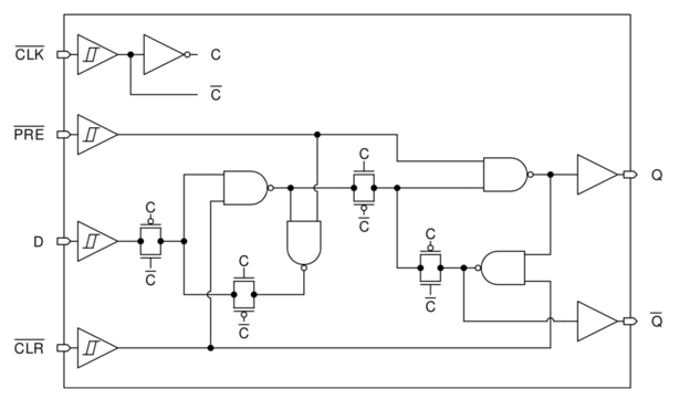
For your reference, I posted a commercial D-Flip Flop (TI SNHCS72). The DRS4 write shift register is a simple array of 8 such registers, with no CLR or PRE, where SROUT is Q of the last Flip Flop.
Best,
Stefan
| Seiya Nozaki wrote: |
|
Dear Stefan,
I have questions about the timing diagram of SROUT/SRIN signal to write/read a write shift register.
1) Value of SRIN signal is saved at the falling edge of SRCLK, correct? (It is written in datasheet, page12, "Bits are latched into the shift register on the falling edge of SRCLK")
2) When are 8-bits of write shift register shown through SROUT? At ridging edges of SRCLK? and with additional delay(~10ns)? or falling edges?
3) In my understanding, when SRCLK is sent to DRS4, we can read and write the values in parallel, right? If so, is it possible just to read the registers without updating the registers?
[Background]
We have two modes to set the write shift register, the first one is to always reconnect to the first line and another one is to reconnect to the same line as when DWRITE goes to Low.
We can read/write the write shift register with the first mode (channel reset, page1). But we rarely face the problem of write shift register, unexpected values are written, with the second mode. With this mode, SROUT signal is sent back to DRS from FPGA as SRIN to write the same value on the write shift register. So there is a small delay(~10ns) due to the routing (DRS->FPGA->DRS, page2). It seems SRIN signal is not stable around the falling edges of SRCLK, thus it could cause that unexpected values are written in write shifter register.
To understand the situation clearly, I'd like to know the answer to the above questions.
Thank you.
Best regards,
Seiya
|
|
| Attachment 1: Screenshot_2020-10-27_at_13.45.39_.png
|
|
|
800
|
Wed Oct 21 15:03:13 2020 |
Seiya Nozaki | Timing diagram of SROUT/SRIN signal to write/read a write shift register | Dear Stefan,
I have questions about the timing diagram of SROUT/SRIN signal to write/read a write shift register.
1) Value of SRIN signal is saved at the falling edge of SRCLK, correct? (It is written in datasheet, page12, "Bits are latched into the shift register on the falling edge of SRCLK")
2) When are 8-bits of write shift register shown through SROUT? At ridging edges of SRCLK? and with additional delay(~10ns)? or falling edges?
3) In my understanding, when SRCLK is sent to DRS4, we can read and write the values in parallel, right? If so, is it possible just to read the registers without updating the registers?
[Background]
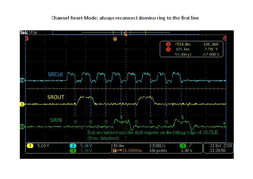
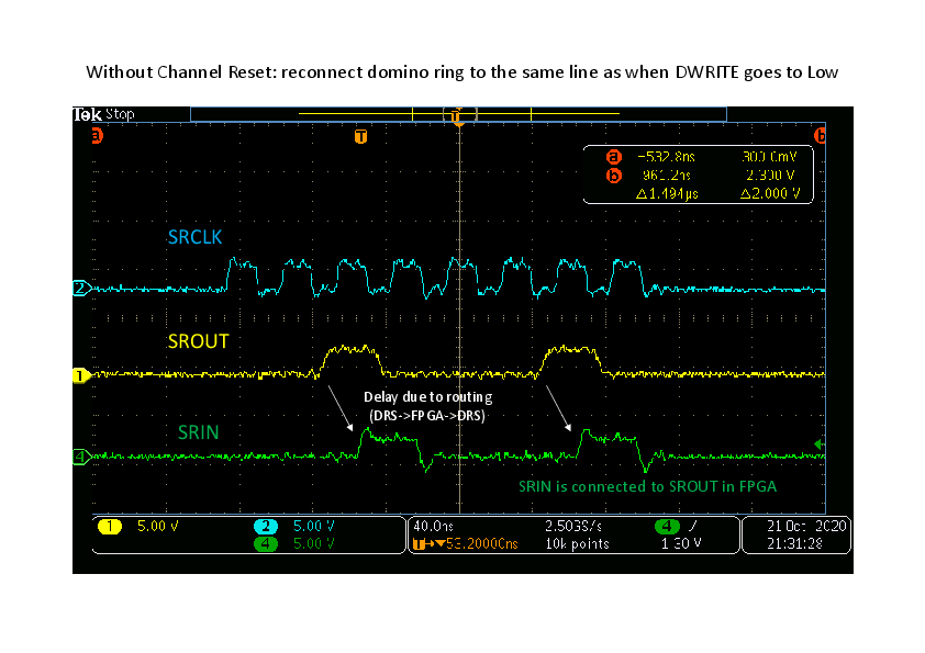
We have two modes to set the write shift register, the first one is to always reconnect to the first line and another one is to reconnect to the same line as when DWRITE goes to Low.
We can read/write the write shift register with the first mode (channel reset, page1). But we rarely face the problem of write shift register, unexpected values are written, with the second mode. With this mode, SROUT signal is sent back to DRS from FPGA as SRIN to write the same value on the write shift register. So there is a small delay(~10ns) due to the routing (DRS->FPGA->DRS, page2). It seems SRIN signal is not stable around the falling edges of SRCLK, thus it could cause that unexpected values are written in write shifter register.
To understand the situation clearly, I'd like to know the answer to the above questions.
Thank you.
Best regards,
Seiya |
| Attachment 1: drs4_srin_srout_srclk.pdf
|
|
|
799
|
Wed Oct 7 11:17:52 2020 |
Elmer Grundeman | External triggering | I will try that, thanks!
| Stefan Ritt wrote: |
|
The trigger is there only to trigger the chip, but cannot be used as a precise time reference. If you want to measure precise timing, do this always BETWEEN two inputs, never between an input and the trigger. You might want to split and delay your trigger signal and feed one copy to another input of the evaluation board as your reference.
Stefan
| Elmer Grundeman wrote: |
|
Dear all,
I had a question about timing jitter and external triggering.
I trigger the board externally with a 3V pulse from a DG645 delay generator and as a test I use the gated charge function to integrate another pulse of the DG which goes into channel 1 (the timing jitter between different outputs of the DG is on the order of ~25 picoseconds).
The issue I’m encountering is that the signal on channel 1 is jittering in time with ~1 ns, which means the signal is jittering with respect to my integration gate (point A and B). If I look at the data it always starts at t = 0.000 but my signal (pulse) moves around in time.
If I don’t use the external trigger but trigger on channel 1 directly the signal does not move with respect to the gate, but I can see the start and end of the trace move in time. If I look at the data the first data point is not at t = 0.000 but some other time, which jitters with ~1 ns.
I did repeat the voltage and timing calibration, but that did not help either.
Do you know where this jitter comes from and if I can get rid of it?
Best regards,
Elmer
|
|
|
|
798
|
Wed Oct 7 10:56:03 2020 |
Stefan Ritt | External triggering | The trigger is there only to trigger the chip, but cannot be used as a precise time reference. If you want to measure precise timing, do this always BETWEEN two inputs, never between an input and the trigger. You might want to split and delay your trigger signal and feed one copy to another input of the evaluation board as your reference.
Stefan
| Elmer Grundeman wrote: |
|
Dear all,
I had a question about timing jitter and external triggering.
I trigger the board externally with a 3V pulse from a DG645 delay generator and as a test I use the gated charge function to integrate another pulse of the DG which goes into channel 1 (the timing jitter between different outputs of the DG is on the order of ~25 picoseconds).
The issue I’m encountering is that the signal on channel 1 is jittering in time with ~1 ns, which means the signal is jittering with respect to my integration gate (point A and B). If I look at the data it always starts at t = 0.000 but my signal (pulse) moves around in time.
If I don’t use the external trigger but trigger on channel 1 directly the signal does not move with respect to the gate, but I can see the start and end of the trace move in time. If I look at the data the first data point is not at t = 0.000 but some other time, which jitters with ~1 ns.
I did repeat the voltage and timing calibration, but that did not help either.
Do you know where this jitter comes from and if I can get rid of it?
Best regards,
Elmer
|
|
|
797
|
Tue Sep 22 17:45:26 2020 |
Elmer Grundeman | External triggering | Dear all,
I had a question about timing jitter and external triggering.
I trigger the board externally with a 3V pulse from a DG645 delay generator and as a test I use the gated charge function to integrate another pulse of the DG which goes into channel 1 (the timing jitter between different outputs of the DG is on the order of ~25 picoseconds).
The issue I’m encountering is that the signal on channel 1 is jittering in time with ~1 ns, which means the signal is jittering with respect to my integration gate (point A and B). If I look at the data it always starts at t = 0.000 but my signal (pulse) moves around in time.
If I don’t use the external trigger but trigger on channel 1 directly the signal does not move with respect to the gate, but I can see the start and end of the trace move in time. If I look at the data the first data point is not at t = 0.000 but some other time, which jitters with ~1 ns.
I did repeat the voltage and timing calibration, but that did not help either.
Do you know where this jitter comes from and if I can get rid of it?
Best regards,
Elmer |
|
796
|
Mon Aug 31 17:17:30 2020 |
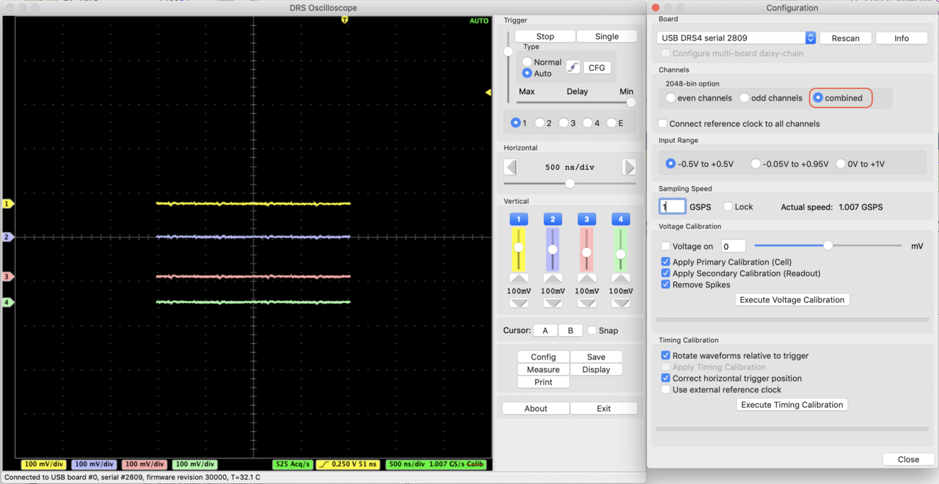
Stefan Ritt | Channel Cascading | If you have a board with cascading option, it should show the "combined" option in the 2048-bin option enabled (not grayed), as in the attached screen shot. If the 2048-bin option is all greyed out, the system does not recognize the cascading option. If your board has a sticker "2048 bin" and you still see the 2048-bin option greyed out, it might mean that a resistor on that board has been forgotten. If you do not see the "2048 bin" sticker on your board, you might not have a board with cascading option. So please check that. If the resistor is really missing, you can send us the board and we will add it.
Stefan
| Hans Steiger wrote: |
|
Dear All,
I have a board with Channel Cascading Option. I have the problem, that it seems to be impossible to run all 4 Channels simultaneously for digitizing pulses. I can just run even or odd channels but not even and odd ones? If I run in combined option, My question: If a board comes with this combined option, is it still usable as a 4Ch Digitizer but with 1024bin traces?
All the best,
Hans
|
|
| Attachment 1: Screenshot_2020-08-31_at_16.52.28_.png
|
|
|
795
|
Mon Aug 31 16:44:12 2020 |
Hans Steiger | Channel Cascading | Dear All,
I have a board with Channel Cascading Option. I have the problem, that it seems to be impossible to run all 4 Channels simultaneously for digitizing pulses. I can just run even or odd channels but not even and odd ones? If I run in combined option, My question: If a board comes with this combined option, is it still usable as a 4Ch Digitizer but with 1024bin traces?
All the best,
Hans |
|
794
|
Mon Aug 31 10:52:42 2020 |
Stefan Ritt | Dynamic Range Evaluation Board and Software | You cannot go below -0.5V for the inputs, since the board does not have an internal negative power supply, which would be necessary for that. If you have -0.8V pulses, the easiest is to use a passive inverter at the input to convert it to a 0.8V pulse.
Stefan
| Hans Steiger wrote: |
|
Dear Evaluation Board Team,
currently I am facing the problem of digitizing pulses with an amplitude of -0.6V to -0.8V. As the dynamic range of the board is 1Vpp, this should be feasible. However, I do not know how to set in the software a correct range. I see only -0.5V/0.5V, and the two positive options. Normally I would use -0.5V/0.5V and give the thing an offset of 0.4V or so? Is this possible? Where can I set such a offset?
All the best,
Hans
|
|
|
793
|
Sat Aug 29 22:00:30 2020 |
Hans Steiger | Dynamic Range Evaluation Board and Software | Dear Evaluation Board Team,
currently I am facing the problem of digitizing pulses with an amplitude of -0.6V to -0.8V. As the dynamic range of the board is 1Vpp, this should be feasible. However, I do not know how to set in the software a correct range. I see only -0.5V/0.5V, and the two positive options. Normally I would use -0.5V/0.5V and give the thing an offset of 0.4V or so? Is this possible? Where can I set such a offset?
All the best,
Hans |
|
792
|
Tue Jul 28 22:40:44 2020 |
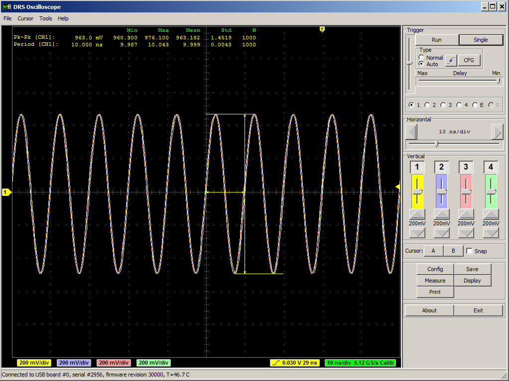
Razvan Stefan Gornea | no board found | I have a very similar problem, the command line doesn't work but the oscilloscope program does! Tried to fix it using Zadig driver update. Using Windows 7....
DRS command line tool, Revision 21435
Type 'help' for a list of available commands.
USB successfully scanned, but no boards found
No DRS Boards found
For completion, I just tested that the test program gives the same error message
C:\Program Files (x86)\DRS\bin>.\drs_exam.exe
USB successfully scanned, but no boards found
No DRS4 evaluation board found
| Stefan Ritt wrote: |
|
"dynamic" or "static" does not matter, as long as you don't use your program on another computer. I have no more idea about the "no board found" problem. It works ok on all computers I tried at our lab.
Stefan
| Lev Pavlov wrote: |
|
Hello. When compiling drs_exam, do you need to use a "static "version of usblib or a "dynamic" version?"The problem with "no board found" is not solved. Thanks for your help.
Lev
|
|
|
| Attachment 1: DRS4_scope.png
|
|
|
791
|
Tue May 26 12:44:16 2020 |
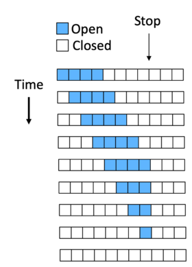
Stefan Ritt | Domino wave | Look at the attached picture. For simplicity, only 4 cells are open and tracking the input signal. Time is flowing from top to bottom. So initially, a train of 4 cells is open. When it's stopped, the train stops not immediately, but kind of "runs against a wall" at the stop cell. So each cell is open for four time ticks effectively, and you can use all 1024 cells.
| xggg wrote: |
|
Hi Stefan,
According to the datasheet DRS_rev09, the write signal is always 16 cells wide. So when the domino wave runs in infinite mode and be stopped by setting DENABLE low , there are always 16 cells capicitors tracking the input signal . It means that the effective sample cells is 1024-16=1008? That's confusing.
|
|
| Attachment 1: Screenshot_2020-05-26_at_12.43.40_.png
|
|
|
790
|
Tue May 26 11:10:27 2020 |
xggg | Domino wave | Hi Stefan,
According to the datasheet DRS_rev09, the write signal is always 16 cells wide. So when the domino wave runs in infinite mode and be stopped by setting DENABLE low , there are always 16 cells capicitors tracking the input signal . It means that the effective sample cells is 1024-16=1008? That's confusing. |
|
789
|
Mon May 25 03:36:12 2020 |
Keita Mizukoshi | DRS4 Evaluation board control tool 'drscl' with macro file | Thank you very much. That is what I wanted.
| Stefan Ritt wrote: |
|
There is an example program in the distribution under software/drscl/drs_exam.cpp which is a stand-alone program to do what you need. It uses the C library coming with the distribution. It configureres the board, defines a trigger, and then writes a few waveforms into a file. You can use it as a starting point for your development. If you need any other language, you have to develop bindings to the C library.
Stefan
| Keita Mizukoshi wrote: |
|
Dear experts,
I would like to use DRS4 evaluation board as DAQ system for small, table-top experiment.
I need waveforms capture as binary file on some trigger based on command line without GUI.
I found `drscl` tool in official software, but it require interactive command. I'd rather use static macro or so on to control DAQ as same behaviour in each time.
I guess, experts are thinking users should develop DAQ code by themselves for their experiment specifically, but my request is very common so someone has already developed these tool.
Best regards,
Keita
|
|
|
|
788
|
Fri May 22 13:24:51 2020 |
Stefan Ritt | Type check at DOFrame.h in official software | The software is a bit outdated, I will soon make a new release.
In meantime, you can replace that like with
bool GetRefclk(int board) { return m_refClk[board]; }
Best,
Stefan
| Keita Mizukoshi wrote: |
|
Hi,
I've failured to compile official software. The cause is the following line.
DOFrame.h L.111 bool GetRefclk() { return m_refClk > 0; }
m_refClk is pointer to bool. I guess these line is for null-check of the pointer.
Can I replace the following line as
bool GetRefclk() { return m_refClk != nullptr; }
?
The latest compilers may not accept C-style check.
My compiler version is
Apple clang version 11.0.3 (clang-1103.0.32.59)
Target: x86_64-apple-darwin19.4.0
Thread model: posix
InstalledDir: /Applications/Xcode.app/Contents/Developer/Toolchains/XcodeDefault.xctoolchain/usr/bin
Best regards,
Keita
|
|
|