 Wed Apr 7 03:29:39 2021, Sean Quinn, Unexpected noise in muxout: t_samp related? Wed Apr 7 03:29:39 2021, Sean Quinn, Unexpected noise in muxout: t_samp related? 
|
Dear DRS4 team,
I'm experiencing some issues that seem to be isolated to the ASIC, and would like to understand if we are doing something wrong. There are several items to address in the post.
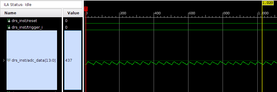
First, I do not think the noise observed is being injected from elsewhere on the board. If I run the DRS in transparent mode, the baseline noise is low, on order 3.5 mV (60 ADU), perhaps radiated from a clock. See below image. The scale is 0 to 1000 ADU with LSB = 6 uV (same AD9245 as eval board.). The DRS is in RUNNING state, I have forced a trigger in the ILA. This is for a single channel, CH0, 1024 cells.
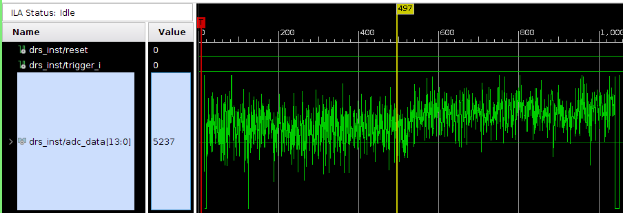
In the next image, I show the waveform obtained from a full readout. This corresponds to ADC_READOUT state, and the plot uses the same 1000 ADU scale. Noise seems around 350 ADU now, many factors worse than before.
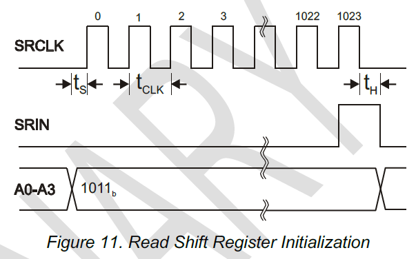
We've spent a lot of time trying to understand what's happening. One area that would be helpful to get some guidance on is the "t_samp" parameter. In Fig. 11 of the data sheet, should there be a t_samp label between t_s and t_clk? It just has arrows there with some width.
In our current firmware I believe R1 is simply one clock after R0 (for both ROI and full readout mode). Would this lead to the added noise observed in muxout?
This leads to the next question on what to actually use for t_samp. In the data sheet, page 4 "Timing Characteristics" it says to use t_samp = t0 + t_clk. Additionally, t0= 10 ns from that table. Fair enough.
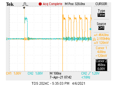
But if I check this against the eval board timing, I see very different values. Here the clock is 15 MHz so t_clk=67 ns (I note another post about this topic https://elog.psi.ch/elogs/DRS4+Forum/713), so I expect t_samp = 77 ns. But in practice it looks like the R0 to R1 delay is ~465 ns? (cyan=RSRLOAD, yellow=SRCLK)
Given this, is t_samp a value that should be tuned by the user?
Best regards,
Sean
|
 Wed Apr 7 08:26:12 2021, Stefan Ritt, Unexpected noise in muxout: t_samp related? Wed Apr 7 08:26:12 2021, Stefan Ritt, Unexpected noise in muxout: t_samp related?
|
Dear Sean,
noise in transparent mode comes from some coupling to your system clock. But 3.5 mV RMS seems rather hight to me. You should get it to below 1 mV if the DRS4 input is clean (try to short it).
The noise in the readout is expected. It looks exactly as Plot3 from the data sheet. You have to calibrate it away with a fixed offset for each cell as described in this paper: https://arxiv.org/abs/1405.4975 (paragraph IV. A. Voltage Calibration).
Concerning t_samp: Fig 11 in the datasheet just tells you that the rising edge of the SRCLK should come later than t_s after the address change. t_s is the setup time and 5 ns. Fig 12 tells you that the ADC should sample the analog output of the DRS t_samp after the address change A0-A3 and t_samp after the rising edge of SRCLK.
The digitizing speed of the evaluation board is indeed 15 MHz instead of the maximum 30 MHz, because this was easier to program in the FPGA. The t_samp has to be there so that the analog output signal of the DRS4 settles to its final value after each SRCLK pulse. If you sample "too early", you sample with the ADC the output when it is sill moving. So you have to wait until the analog is settled, but just before the next DRS sample becomes visible at the output. You can fine tune this with a differential probe at the DRS4 analog output (on a single ended probe you might drown in noise) on one channel of yoru scope and the ADC sample clock on the other channel of your scope. Note that the ADC sample clock cannot be derived straight from your FPGA clock, but you need some clock manager to fine-adjust its phase in 1ns steps.
But again, looking at your output, everything seems fine. You see the 5mV rms noise indicated in the datasheet table 1, which translates to about 20 mV peak-to-peak. If you do the offset calibration, this should go down to below 1 mV.
Best,
Stefan
| Sean Quinn wrote: |
|
Dear DRS4 team,
I'm experiencing some issues that seem to be isolated to the ASIC, and would like to understand if we are doing something wrong. There are several items to address in the post.
First, I do not think the noise observed is being injected from elsewhere on the board. If I run the DRS in transparent mode, the baseline noise is low, on order 3.5 mV (60 ADU), perhaps radiated from a clock. See below image. The scale is 0 to 1000 ADU with LSB = 6 uV (same AD9245 as eval board.). The DRS is in RUNNING state, I have forced a trigger in the ILA. This is for a single channel, CH0, 1024 cells.
In the next image, I show the waveform obtained from a full readout. This corresponds to ADC_READOUT state, and the plot uses the same 1000 ADU scale. Noise seems around 350 ADU now, many factors worse than before.
We've spent a lot of time trying to understand what's happening. One area that would be helpful to get some guidance on is the "t_samp" parameter. In Fig. 11 of the data sheet, should there be a t_samp label between t_s and t_clk? It just has arrows there with some width.
In our current firmware I believe R1 is simply one clock after R0 (for both ROI and full readout mode). Would this lead to the added noise observed in muxout?
This leads to the next question on what to actually use for t_samp. In the data sheet, page 4 "Timing Characteristics" it says to use t_samp = t0 + t_clk. Additionally, t0= 10 ns from that table. Fair enough.
But if I check this against the eval board timing, I see very different values. Here the clock is 15 MHz so t_clk=67 ns (I note another post about this topic https://elog.psi.ch/elogs/DRS4+Forum/713), so I expect t_samp = 77 ns. But in practice it looks like the R0 to R1 delay is ~465 ns? (cyan=RSRLOAD, yellow=SRCLK)
Given this, is t_samp a value that should be tuned by the user?
Best regards,
Sean
|
|
|
Fri Apr 9 20:22:13 2021, Sean Quinn, Unexpected noise in muxout: t_samp related?
|
Hi Stefan,
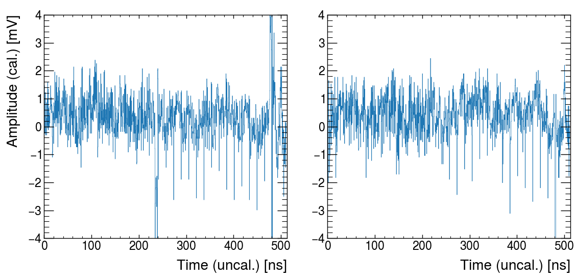
Thanks much for the quick reply. Ok, yes, things do seem ok after the offset calibration. I am running into some other issues I could use your advice on but will make a separate thread. As a preview, you can see hints in this waveform (periodic negative spikes).
This one should be considered resolved.
| Stefan Ritt wrote: |
|
Dear Sean,
noise in transparent mode comes from some coupling to your system clock. But 3.5 mV RMS seems rather hight to me. You should get it to below 1 mV if the DRS4 input is clean (try to short it).
The noise in the readout is expected. It looks exactly as Plot3 from the data sheet. You have to calibrate it away with a fixed offset for each cell as described in this paper: https://arxiv.org/abs/1405.4975 (paragraph IV. A. Voltage Calibration).
Concerning t_samp: Fig 11 in the datasheet just tells you that the rising edge of the SRCLK should come later than t_s after the address change. t_s is the setup time and 5 ns. Fig 12 tells you that the ADC should sample the analog output of the DRS t_samp after the address change A0-A3 and t_samp after the rising edge of SRCLK.
The digitizing speed of the evaluation board is indeed 15 MHz instead of the maximum 30 MHz, because this was easier to program in the FPGA. The t_samp has to be there so that the analog output signal of the DRS4 settles to its final value after each SRCLK pulse. If you sample "too early", you sample with the ADC the output when it is sill moving. So you have to wait until the analog is settled, but just before the next DRS sample becomes visible at the output. You can fine tune this with a differential probe at the DRS4 analog output (on a single ended probe you might drown in noise) on one channel of yoru scope and the ADC sample clock on the other channel of your scope. Note that the ADC sample clock cannot be derived straight from your FPGA clock, but you need some clock manager to fine-adjust its phase in 1ns steps.
But again, looking at your output, everything seems fine. You see the 5mV rms noise indicated in the datasheet table 1, which translates to about 20 mV peak-to-peak. If you do the offset calibration, this should go down to below 1 mV.
Best,
Stefan
| Sean Quinn wrote: |
|
Dear DRS4 team,
I'm experiencing some issues that seem to be isolated to the ASIC, and would like to understand if we are doing something wrong. There are several items to address in the post.
First, I do not think the noise observed is being injected from elsewhere on the board. If I run the DRS in transparent mode, the baseline noise is low, on order 3.5 mV (60 ADU), perhaps radiated from a clock. See below image. The scale is 0 to 1000 ADU with LSB = 6 uV (same AD9245 as eval board.). The DRS is in RUNNING state, I have forced a trigger in the ILA. This is for a single channel, CH0, 1024 cells.
In the next image, I show the waveform obtained from a full readout. This corresponds to ADC_READOUT state, and the plot uses the same 1000 ADU scale. Noise seems around 350 ADU now, many factors worse than before.
We've spent a lot of time trying to understand what's happening. One area that would be helpful to get some guidance on is the "t_samp" parameter. In Fig. 11 of the data sheet, should there be a t_samp label between t_s and t_clk? It just has arrows there with some width.
In our current firmware I believe R1 is simply one clock after R0 (for both ROI and full readout mode). Would this lead to the added noise observed in muxout?
This leads to the next question on what to actually use for t_samp. In the data sheet, page 4 "Timing Characteristics" it says to use t_samp = t0 + t_clk. Additionally, t0= 10 ns from that table. Fair enough.
But if I check this against the eval board timing, I see very different values. Here the clock is 15 MHz so t_clk=67 ns (I note another post about this topic https://elog.psi.ch/elogs/DRS4+Forum/713), so I expect t_samp = 77 ns. But in practice it looks like the R0 to R1 delay is ~465 ns? (cyan=RSRLOAD, yellow=SRCLK)
Given this, is t_samp a value that should be tuned by the user?
Best regards,
Sean
|
|
|
|
Fri Apr 9 20:55:28 2021, Stefan Ritt, Unexpected noise in muxout: t_samp related?
|
If you do the cell calibration correctly, your noise should be ~0.4 mV. You seem to be 2-3x larger. The periodic negative spikes come if you dont' sample at the right time. Adjust t_samp until they are gone.
Stefan
| Sean Quinn wrote: |
|
Hi Stefan,
Thanks much for the quick reply. Ok, yes, things do seem ok after the offset calibration. I am running into some other issues I could use your advice on but will make a separate thread. As a preview, you can see hints in this waveform (periodic negative spikes).
This one should be considered resolved.
| Stefan Ritt wrote: |
|
Dear Sean,
noise in transparent mode comes from some coupling to your system clock. But 3.5 mV RMS seems rather hight to me. You should get it to below 1 mV if the DRS4 input is clean (try to short it).
The noise in the readout is expected. It looks exactly as Plot3 from the data sheet. You have to calibrate it away with a fixed offset for each cell as described in this paper: https://arxiv.org/abs/1405.4975 (paragraph IV. A. Voltage Calibration).
Concerning t_samp: Fig 11 in the datasheet just tells you that the rising edge of the SRCLK should come later than t_s after the address change. t_s is the setup time and 5 ns. Fig 12 tells you that the ADC should sample the analog output of the DRS t_samp after the address change A0-A3 and t_samp after the rising edge of SRCLK.
The digitizing speed of the evaluation board is indeed 15 MHz instead of the maximum 30 MHz, because this was easier to program in the FPGA. The t_samp has to be there so that the analog output signal of the DRS4 settles to its final value after each SRCLK pulse. If you sample "too early", you sample with the ADC the output when it is sill moving. So you have to wait until the analog is settled, but just before the next DRS sample becomes visible at the output. You can fine tune this with a differential probe at the DRS4 analog output (on a single ended probe you might drown in noise) on one channel of yoru scope and the ADC sample clock on the other channel of your scope. Note that the ADC sample clock cannot be derived straight from your FPGA clock, but you need some clock manager to fine-adjust its phase in 1ns steps.
But again, looking at your output, everything seems fine. You see the 5mV rms noise indicated in the datasheet table 1, which translates to about 20 mV peak-to-peak. If you do the offset calibration, this should go down to below 1 mV.
Best,
Stefan
| Sean Quinn wrote: |
|
Dear DRS4 team,
I'm experiencing some issues that seem to be isolated to the ASIC, and would like to understand if we are doing something wrong. There are several items to address in the post.
First, I do not think the noise observed is being injected from elsewhere on the board. If I run the DRS in transparent mode, the baseline noise is low, on order 3.5 mV (60 ADU), perhaps radiated from a clock. See below image. The scale is 0 to 1000 ADU with LSB = 6 uV (same AD9245 as eval board.). The DRS is in RUNNING state, I have forced a trigger in the ILA. This is for a single channel, CH0, 1024 cells.
In the next image, I show the waveform obtained from a full readout. This corresponds to ADC_READOUT state, and the plot uses the same 1000 ADU scale. Noise seems around 350 ADU now, many factors worse than before.
We've spent a lot of time trying to understand what's happening. One area that would be helpful to get some guidance on is the "t_samp" parameter. In Fig. 11 of the data sheet, should there be a t_samp label between t_s and t_clk? It just has arrows there with some width.
In our current firmware I believe R1 is simply one clock after R0 (for both ROI and full readout mode). Would this lead to the added noise observed in muxout?
This leads to the next question on what to actually use for t_samp. In the data sheet, page 4 "Timing Characteristics" it says to use t_samp = t0 + t_clk. Additionally, t0= 10 ns from that table. Fair enough.
But if I check this against the eval board timing, I see very different values. Here the clock is 15 MHz so t_clk=67 ns (I note another post about this topic https://elog.psi.ch/elogs/DRS4+Forum/713), so I expect t_samp = 77 ns. But in practice it looks like the R0 to R1 delay is ~465 ns? (cyan=RSRLOAD, yellow=SRCLK)
Given this, is t_samp a value that should be tuned by the user?
Best regards,
Sean
|
|
|
|
|
Fri Apr 9 21:56:54 2021, Sean Quinn, Unexpected noise in muxout: t_samp related?
|
Yes, there is some systematic board noise on this prototype, unfortunately 
Ok, then it seems the other post I made might still belong in this thread after all.
Thanks for confirming negative spike behavior, we now have a mitigation plan going forward.
Cheers,
| Stefan Ritt wrote: |
|
If you do the cell calibration correctly, your noise should be ~0.4 mV. You seem to be 2-3x larger. The periodic negative spikes come if you dont' sample at the right time. Adjust t_samp until they are gone.
Stefan
| Sean Quinn wrote: |
|
Hi Stefan,
Thanks much for the quick reply. Ok, yes, things do seem ok after the offset calibration. I am running into some other issues I could use your advice on but will make a separate thread. As a preview, you can see hints in this waveform (periodic negative spikes).
This one should be considered resolved.
| Stefan Ritt wrote: |
|
Dear Sean,
noise in transparent mode comes from some coupling to your system clock. But 3.5 mV RMS seems rather hight to me. You should get it to below 1 mV if the DRS4 input is clean (try to short it).
The noise in the readout is expected. It looks exactly as Plot3 from the data sheet. You have to calibrate it away with a fixed offset for each cell as described in this paper: https://arxiv.org/abs/1405.4975 (paragraph IV. A. Voltage Calibration).
Concerning t_samp: Fig 11 in the datasheet just tells you that the rising edge of the SRCLK should come later than t_s after the address change. t_s is the setup time and 5 ns. Fig 12 tells you that the ADC should sample the analog output of the DRS t_samp after the address change A0-A3 and t_samp after the rising edge of SRCLK.
The digitizing speed of the evaluation board is indeed 15 MHz instead of the maximum 30 MHz, because this was easier to program in the FPGA. The t_samp has to be there so that the analog output signal of the DRS4 settles to its final value after each SRCLK pulse. If you sample "too early", you sample with the ADC the output when it is sill moving. So you have to wait until the analog is settled, but just before the next DRS sample becomes visible at the output. You can fine tune this with a differential probe at the DRS4 analog output (on a single ended probe you might drown in noise) on one channel of yoru scope and the ADC sample clock on the other channel of your scope. Note that the ADC sample clock cannot be derived straight from your FPGA clock, but you need some clock manager to fine-adjust its phase in 1ns steps.
But again, looking at your output, everything seems fine. You see the 5mV rms noise indicated in the datasheet table 1, which translates to about 20 mV peak-to-peak. If you do the offset calibration, this should go down to below 1 mV.
Best,
Stefan
| Sean Quinn wrote: |
|
Dear DRS4 team,
I'm experiencing some issues that seem to be isolated to the ASIC, and would like to understand if we are doing something wrong. There are several items to address in the post.
First, I do not think the noise observed is being injected from elsewhere on the board. If I run the DRS in transparent mode, the baseline noise is low, on order 3.5 mV (60 ADU), perhaps radiated from a clock. See below image. The scale is 0 to 1000 ADU with LSB = 6 uV (same AD9245 as eval board.). The DRS is in RUNNING state, I have forced a trigger in the ILA. This is for a single channel, CH0, 1024 cells.
In the next image, I show the waveform obtained from a full readout. This corresponds to ADC_READOUT state, and the plot uses the same 1000 ADU scale. Noise seems around 350 ADU now, many factors worse than before.
We've spent a lot of time trying to understand what's happening. One area that would be helpful to get some guidance on is the "t_samp" parameter. In Fig. 11 of the data sheet, should there be a t_samp label between t_s and t_clk? It just has arrows there with some width.
In our current firmware I believe R1 is simply one clock after R0 (for both ROI and full readout mode). Would this lead to the added noise observed in muxout?
This leads to the next question on what to actually use for t_samp. In the data sheet, page 4 "Timing Characteristics" it says to use t_samp = t0 + t_clk. Additionally, t0= 10 ns from that table. Fair enough.
But if I check this against the eval board timing, I see very different values. Here the clock is 15 MHz so t_clk=67 ns (I note another post about this topic https://elog.psi.ch/elogs/DRS4+Forum/713), so I expect t_samp = 77 ns. But in practice it looks like the R0 to R1 delay is ~465 ns? (cyan=RSRLOAD, yellow=SRCLK)
Given this, is t_samp a value that should be tuned by the user?
Best regards,
Sean
|
|
|
|
|
|
Thu Feb 25 17:56:39 2021, Matthias Plum, DRS spike removal for multiple waveforms
|
Hi,
Is there a way that someone can help me and my student to enable RemoveSymmetricSpikes function in the drs_exam.cpp? We are not 100% sure how to call the function if you want to read out four waveforms.
Cheers,
Matthias |
|
Fri Feb 26 08:52:50 2021, Stefan Ritt, DRS spike removal for multiple waveforms
|
Just look at the definition of the function below, all parameters are explained there. In meantime we have a firmware fix to avoid the spikes inside the chip, but I have not yet found time to update the evaluation board.
Stefan
void DRSBoard::RemoveSymmetricSpikes(short **wf, int nwf,
short diffThreshold, int spikeWidth,
short maxPeakToPeak, short spikeVoltage,
int nTimeRegionThreshold)
{
// Remove a specific kind of spike on DRS4.
// This spike has some features,
// - Common on all the channels on a chip
// - Constant heigh and width
// - Two spikes per channel
// - Symmetric to cell #0.
//
// This is not general purpose spike-removing function.
//
// wf : Waveform data. cell#0 must be at bin0,
// and number of bins must be kNumberOfBins.
// nwf : Number of channels which "wf" holds.
// diffThreshold : Amplitude threshold to find peak
// spikeWidth : Width of spike
// maxPeakToPeak : When peak-to-peak is larger than this, the channel
// is not used to find spikes.
// spikeVoltage : Amplitude of spikes. When it is 0, it is calculated in this function
// from voltage difference from neighboring bins.
// nTimeRegionThreshold : Requirement of number of time regions having spike at common position.
// Total number of time regions is 2*"nwf". |
|
Wed Jan 20 12:14:49 2021, Taegyu Lee, drs4 persistence
|
Dear all,
I have a question about the function that drs4 can perform.
Is there any function in drs4 that is analogous to that of "persistence display" in oscilloscope?? (accumulating pulses)
Thank you |
|
Wed Jan 20 17:37:51 2021, Stefan Ritt, drs4 persistence
|
The chip itself can only sample a single waveform, that must be done in the attached software. The current DRSOscilloscope software coming with the evaluation board has not yet implemented that, but if you write your own software you can do so.
| Taegyu Lee wrote: |
|
Dear all,
I have a question about the function that drs4 can perform.
Is there any function in drs4 that is analogous to that of "persistence display" in oscilloscope?? (accumulating pulses)
Thank you
|
|
|
Thu Dec 17 09:29:43 2020, Alex Myczko, drs sources on github?
|
Are there plans to add the drs software to github? (asking because I have users @ethz.ch that want to use it on debian,
thus I'm creating official debian packages of it, if license allows so, but talking to upstream (the developers) would be
much easier on github (or irc) than on this "DRS4 Discussion Forum".

Best, |
|
Thu Dec 17 11:31:34 2020, Stefan Ritt, drs sources on github?
|
Not github, but bitbucket: https://bitbucket.org/ritt/drs4eb/src/master/

But development kind of stalled, so there will be updates only in case of severe bugs, which are kind of gone after 10 years now.

Best,
Stefan

> Are there plans to add the drs software to github? (asking because I have users @ethz.ch that want to use it on debian,
> thus I'm creating official debian packages of it, if license allows so, but talking to upstream (the developers) would be
> much easier on github (or irc) than on this "DRS4 Discussion Forum".
>
> Best, |
|
Wed Oct 21 15:03:13 2020, Seiya Nozaki, Timing diagram of SROUT/SRIN signal to write/read a write shift register
|
Dear Stefan,
I have questions about the timing diagram of SROUT/SRIN signal to write/read a write shift register.
1) Value of SRIN signal is saved at the falling edge of SRCLK, correct? (It is written in datasheet, page12, "Bits are latched into the shift register on the falling edge of SRCLK")
2) When are 8-bits of write shift register shown through SROUT? At ridging edges of SRCLK? and with additional delay(~10ns)? or falling edges?
3) In my understanding, when SRCLK is sent to DRS4, we can read and write the values in parallel, right? If so, is it possible just to read the registers without updating the registers?
[Background]
We have two modes to set the write shift register, the first one is to always reconnect to the first line and another one is to reconnect to the same line as when DWRITE goes to Low.
We can read/write the write shift register with the first mode (channel reset, page1). But we rarely face the problem of write shift register, unexpected values are written, with the second mode. With this mode, SROUT signal is sent back to DRS from FPGA as SRIN to write the same value on the write shift register. So there is a small delay(~10ns) due to the routing (DRS->FPGA->DRS, page2). It seems SRIN signal is not stable around the falling edges of SRCLK, thus it could cause that unexpected values are written in write shifter register.
To understand the situation clearly, I'd like to know the answer to the above questions.
Thank you.
Best regards,
Seiya |
|
Tue Oct 27 13:37:23 2020, Stefan Ritt, Timing diagram of SROUT/SRIN signal to write/read a write shift register
|
Dear Seiya,
1) That's correct. SRIN is ampled at the falling edge. Pleae make sure to obey the hold-time as written in the datasheet. P.12, Fig. 11: SRIN must be stable before the falling edge of SRCLK and tH after the falling clock. tH is 5ns according to table 1.
2) The write shift register is a 8-bit shift register, with an input, output and clock. After the first clock pulse, the 7th bit is shown, after the second clock pulse the 6th bit and so on. You you need 8 clock pulses to read the whole register. At the same time you write to the register, so what ever is present at SRIN will replace the old 8 bits of that register.
3) No this is not possible. When you read the register, you write to it at the same time. One possibilty is to connect SROUT to SRIN during that (maybe via the FPGA). Then you have a circular register wich is the same after each 8 clock pulses.
For your reference, I posted a commercial D-Flip Flop (TI SNHCS72). The DRS4 write shift register is a simple array of 8 such registers, with no CLR or PRE, where SROUT is Q of the last Flip Flop.
Best,
Stefan
| Seiya Nozaki wrote: |
|
Dear Stefan,
I have questions about the timing diagram of SROUT/SRIN signal to write/read a write shift register.
1) Value of SRIN signal is saved at the falling edge of SRCLK, correct? (It is written in datasheet, page12, "Bits are latched into the shift register on the falling edge of SRCLK")
2) When are 8-bits of write shift register shown through SROUT? At ridging edges of SRCLK? and with additional delay(~10ns)? or falling edges?
3) In my understanding, when SRCLK is sent to DRS4, we can read and write the values in parallel, right? If so, is it possible just to read the registers without updating the registers?
[Background]
We have two modes to set the write shift register, the first one is to always reconnect to the first line and another one is to reconnect to the same line as when DWRITE goes to Low.
We can read/write the write shift register with the first mode (channel reset, page1). But we rarely face the problem of write shift register, unexpected values are written, with the second mode. With this mode, SROUT signal is sent back to DRS from FPGA as SRIN to write the same value on the write shift register. So there is a small delay(~10ns) due to the routing (DRS->FPGA->DRS, page2). It seems SRIN signal is not stable around the falling edges of SRCLK, thus it could cause that unexpected values are written in write shifter register.
To understand the situation clearly, I'd like to know the answer to the above questions.
Thank you.
Best regards,
Seiya
|
|
|
Tue Oct 27 15:02:09 2020, Seiya Nozaki, Timing diagram of SROUT/SRIN signal to write/read a write shift register
|
Dear Stefan,
Thank you for your reply.
SRIN is directly connected to SROUT via FPGA for now, but it is unstable for the timing between clock and SRIN depending on the firmware logic.
We want to make our system more robust, so we are thinking to use a clock with a lower frequency (let's say 16.6 MHz) or change the duty cycle of a clock to keep more time between the rising edge and falling edge of a clock. This change is just for reading/writing the write shift register, we will use a 33 MHz clock for the analog readout in any case.
If we change like above, are there any concerns from the DRS4 side?
Best,
Seiya
| Stefan Ritt wrote: |
|
Dear Seiya,
1) That's correct. SRIN is ampled at the falling edge. Pleae make sure to obey the hold-time as written in the datasheet. P.12, Fig. 11: SRIN must be stable before the falling edge of SRCLK and tH after the falling clock. tH is 5ns according to table 1.
2) The write shift register is a 8-bit shift register, with an input, output and clock. After the first clock pulse, the 7th bit is shown, after the second clock pulse the 6th bit and so on. You you need 8 clock pulses to read the whole register. At the same time you write to the register, so what ever is present at SRIN will replace the old 8 bits of that register.
3) No this is not possible. When you read the register, you write to it at the same time. One possibilty is to connect SROUT to SRIN during that (maybe via the FPGA). Then you have a circular register wich is the same after each 8 clock pulses.
For your reference, I posted a commercial D-Flip Flop (TI SNHCS72). The DRS4 write shift register is a simple array of 8 such registers, with no CLR or PRE, where SROUT is Q of the last Flip Flop.
Best,
Stefan
| Seiya Nozaki wrote: |
|
Dear Stefan,
I have questions about the timing diagram of SROUT/SRIN signal to write/read a write shift register.
1) Value of SRIN signal is saved at the falling edge of SRCLK, correct? (It is written in datasheet, page12, "Bits are latched into the shift register on the falling edge of SRCLK")
2) When are 8-bits of write shift register shown through SROUT? At ridging edges of SRCLK? and with additional delay(~10ns)? or falling edges?
3) In my understanding, when SRCLK is sent to DRS4, we can read and write the values in parallel, right? If so, is it possible just to read the registers without updating the registers?
[Background]
We have two modes to set the write shift register, the first one is to always reconnect to the first line and another one is to reconnect to the same line as when DWRITE goes to Low.
We can read/write the write shift register with the first mode (channel reset, page1). But we rarely face the problem of write shift register, unexpected values are written, with the second mode. With this mode, SROUT signal is sent back to DRS from FPGA as SRIN to write the same value on the write shift register. So there is a small delay(~10ns) due to the routing (DRS->FPGA->DRS, page2). It seems SRIN signal is not stable around the falling edges of SRCLK, thus it could cause that unexpected values are written in write shifter register.
To understand the situation clearly, I'd like to know the answer to the above questions.
Thank you.
Best regards,
Seiya
|
|
|
|
Tue Oct 27 15:24:38 2020, Stefan Ritt, Timing diagram of SROUT/SRIN signal to write/read a write shift register
|
This is a static shift register, so you can make the clock as slow as you want. Actually I don't use a "clock", I just use a data pin I control via a state machine in the VHDL code. This way I have more control over the edges. I need several (internal) clock cycles to produce one SRCLK clock cycle, but that does not matter for the DRS.
Stefan
| Seiya Nozaki wrote: |
|
Dear Stefan,
Thank you for your reply.
SRIN is directly connected to SROUT via FPGA for now, but it is unstable for the timing between clock and SRIN depending on the firmware logic.
We want to make our system more robust, so we are thinking to use a clock with a lower frequency (let's say 16.6 MHz) or change the duty cycle of a clock to keep more time between the rising edge and falling edge of a clock. This change is just for reading/writing the write shift register, we will use a 33 MHz clock for the analog readout in any case.
If we change like above, are there any concerns from the DRS4 side?
Best,
Seiya
| Stefan Ritt wrote: |
|
Dear Seiya,
1) That's correct. SRIN is ampled at the falling edge. Pleae make sure to obey the hold-time as written in the datasheet. P.12, Fig. 11: SRIN must be stable before the falling edge of SRCLK and tH after the falling clock. tH is 5ns according to table 1.
2) The write shift register is a 8-bit shift register, with an input, output and clock. After the first clock pulse, the 7th bit is shown, after the second clock pulse the 6th bit and so on. You you need 8 clock pulses to read the whole register. At the same time you write to the register, so what ever is present at SRIN will replace the old 8 bits of that register.
3) No this is not possible. When you read the register, you write to it at the same time. One possibilty is to connect SROUT to SRIN during that (maybe via the FPGA). Then you have a circular register wich is the same after each 8 clock pulses.
For your reference, I posted a commercial D-Flip Flop (TI SNHCS72). The DRS4 write shift register is a simple array of 8 such registers, with no CLR or PRE, where SROUT is Q of the last Flip Flop.
Best,
Stefan
| Seiya Nozaki wrote: |
|
Dear Stefan,
I have questions about the timing diagram of SROUT/SRIN signal to write/read a write shift register.
1) Value of SRIN signal is saved at the falling edge of SRCLK, correct? (It is written in datasheet, page12, "Bits are latched into the shift register on the falling edge of SRCLK")
2) When are 8-bits of write shift register shown through SROUT? At ridging edges of SRCLK? and with additional delay(~10ns)? or falling edges?
3) In my understanding, when SRCLK is sent to DRS4, we can read and write the values in parallel, right? If so, is it possible just to read the registers without updating the registers?
[Background]
We have two modes to set the write shift register, the first one is to always reconnect to the first line and another one is to reconnect to the same line as when DWRITE goes to Low.
We can read/write the write shift register with the first mode (channel reset, page1). But we rarely face the problem of write shift register, unexpected values are written, with the second mode. With this mode, SROUT signal is sent back to DRS from FPGA as SRIN to write the same value on the write shift register. So there is a small delay(~10ns) due to the routing (DRS->FPGA->DRS, page2). It seems SRIN signal is not stable around the falling edges of SRCLK, thus it could cause that unexpected values are written in write shifter register.
To understand the situation clearly, I'd like to know the answer to the above questions.
Thank you.
Best regards,
Seiya
|
|
|
|
|
Wed Oct 28 04:32:19 2020, Seiya Nozaki, Timing diagram of SROUT/SRIN signal to write/read a write shift register
|
Dear Stefan,
OK, it's good to hear! Thank you!
Best,
Seiya
| Stefan Ritt wrote: |
|
This is a static shift register, so you can make the clock as slow as you want. Actually I don't use a "clock", I just use a data pin I control via a state machine in the VHDL code. This way I have more control over the edges. I need several (internal) clock cycles to produce one SRCLK clock cycle, but that does not matter for the DRS.
Stefan
| Seiya Nozaki wrote: |
|
Dear Stefan,
Thank you for your reply.
SRIN is directly connected to SROUT via FPGA for now, but it is unstable for the timing between clock and SRIN depending on the firmware logic.
We want to make our system more robust, so we are thinking to use a clock with a lower frequency (let's say 16.6 MHz) or change the duty cycle of a clock to keep more time between the rising edge and falling edge of a clock. This change is just for reading/writing the write shift register, we will use a 33 MHz clock for the analog readout in any case.
If we change like above, are there any concerns from the DRS4 side?
Best,
Seiya
| Stefan Ritt wrote: |
|
Dear Seiya,
1) That's correct. SRIN is ampled at the falling edge. Pleae make sure to obey the hold-time as written in the datasheet. P.12, Fig. 11: SRIN must be stable before the falling edge of SRCLK and tH after the falling clock. tH is 5ns according to table 1.
2) The write shift register is a 8-bit shift register, with an input, output and clock. After the first clock pulse, the 7th bit is shown, after the second clock pulse the 6th bit and so on. You you need 8 clock pulses to read the whole register. At the same time you write to the register, so what ever is present at SRIN will replace the old 8 bits of that register.
3) No this is not possible. When you read the register, you write to it at the same time. One possibilty is to connect SROUT to SRIN during that (maybe via the FPGA). Then you have a circular register wich is the same after each 8 clock pulses.
For your reference, I posted a commercial D-Flip Flop (TI SNHCS72). The DRS4 write shift register is a simple array of 8 such registers, with no CLR or PRE, where SROUT is Q of the last Flip Flop.
Best,
Stefan
| Seiya Nozaki wrote: |
|
Dear Stefan,
I have questions about the timing diagram of SROUT/SRIN signal to write/read a write shift register.
1) Value of SRIN signal is saved at the falling edge of SRCLK, correct? (It is written in datasheet, page12, "Bits are latched into the shift register on the falling edge of SRCLK")
2) When are 8-bits of write shift register shown through SROUT? At ridging edges of SRCLK? and with additional delay(~10ns)? or falling edges?
3) In my understanding, when SRCLK is sent to DRS4, we can read and write the values in parallel, right? If so, is it possible just to read the registers without updating the registers?
[Background]
We have two modes to set the write shift register, the first one is to always reconnect to the first line and another one is to reconnect to the same line as when DWRITE goes to Low.
We can read/write the write shift register with the first mode (channel reset, page1). But we rarely face the problem of write shift register, unexpected values are written, with the second mode. With this mode, SROUT signal is sent back to DRS from FPGA as SRIN to write the same value on the write shift register. So there is a small delay(~10ns) due to the routing (DRS->FPGA->DRS, page2). It seems SRIN signal is not stable around the falling edges of SRCLK, thus it could cause that unexpected values are written in write shifter register.
To understand the situation clearly, I'd like to know the answer to the above questions.
Thank you.
Best regards,
Seiya
|
|
|
|
|
|
Tue Sep 22 17:45:26 2020, Elmer Grundeman, External triggering
|
Dear all,
I had a question about timing jitter and external triggering.
I trigger the board externally with a 3V pulse from a DG645 delay generator and as a test I use the gated charge function to integrate another pulse of the DG which goes into channel 1 (the timing jitter between different outputs of the DG is on the order of ~25 picoseconds).
The issue I’m encountering is that the signal on channel 1 is jittering in time with ~1 ns, which means the signal is jittering with respect to my integration gate (point A and B). If I look at the data it always starts at t = 0.000 but my signal (pulse) moves around in time.
If I don’t use the external trigger but trigger on channel 1 directly the signal does not move with respect to the gate, but I can see the start and end of the trace move in time. If I look at the data the first data point is not at t = 0.000 but some other time, which jitters with ~1 ns.
I did repeat the voltage and timing calibration, but that did not help either.
Do you know where this jitter comes from and if I can get rid of it?
Best regards,
Elmer |
|
Wed Oct 7 10:56:03 2020, Stefan Ritt, External triggering
|
The trigger is there only to trigger the chip, but cannot be used as a precise time reference. If you want to measure precise timing, do this always BETWEEN two inputs, never between an input and the trigger. You might want to split and delay your trigger signal and feed one copy to another input of the evaluation board as your reference.
Stefan
| Elmer Grundeman wrote: |
|
Dear all,
I had a question about timing jitter and external triggering.
I trigger the board externally with a 3V pulse from a DG645 delay generator and as a test I use the gated charge function to integrate another pulse of the DG which goes into channel 1 (the timing jitter between different outputs of the DG is on the order of ~25 picoseconds).
The issue I’m encountering is that the signal on channel 1 is jittering in time with ~1 ns, which means the signal is jittering with respect to my integration gate (point A and B). If I look at the data it always starts at t = 0.000 but my signal (pulse) moves around in time.
If I don’t use the external trigger but trigger on channel 1 directly the signal does not move with respect to the gate, but I can see the start and end of the trace move in time. If I look at the data the first data point is not at t = 0.000 but some other time, which jitters with ~1 ns.
I did repeat the voltage and timing calibration, but that did not help either.
Do you know where this jitter comes from and if I can get rid of it?
Best regards,
Elmer
|
|
|
Wed Oct 7 11:17:52 2020, Elmer Grundeman, External triggering
|
I will try that, thanks!
| Stefan Ritt wrote: |
|
The trigger is there only to trigger the chip, but cannot be used as a precise time reference. If you want to measure precise timing, do this always BETWEEN two inputs, never between an input and the trigger. You might want to split and delay your trigger signal and feed one copy to another input of the evaluation board as your reference.
Stefan
| Elmer Grundeman wrote: |
|
Dear all,
I had a question about timing jitter and external triggering.
I trigger the board externally with a 3V pulse from a DG645 delay generator and as a test I use the gated charge function to integrate another pulse of the DG which goes into channel 1 (the timing jitter between different outputs of the DG is on the order of ~25 picoseconds).
The issue I’m encountering is that the signal on channel 1 is jittering in time with ~1 ns, which means the signal is jittering with respect to my integration gate (point A and B). If I look at the data it always starts at t = 0.000 but my signal (pulse) moves around in time.
If I don’t use the external trigger but trigger on channel 1 directly the signal does not move with respect to the gate, but I can see the start and end of the trace move in time. If I look at the data the first data point is not at t = 0.000 but some other time, which jitters with ~1 ns.
I did repeat the voltage and timing calibration, but that did not help either.
Do you know where this jitter comes from and if I can get rid of it?
Best regards,
Elmer
|
|
|
|
Mon Aug 31 16:44:12 2020, Hans Steiger, Channel Cascading
|
Dear All,
I have a board with Channel Cascading Option. I have the problem, that it seems to be impossible to run all 4 Channels simultaneously for digitizing pulses. I can just run even or odd channels but not even and odd ones? If I run in combined option, My question: If a board comes with this combined option, is it still usable as a 4Ch Digitizer but with 1024bin traces?
All the best,
Hans |
|
Mon Aug 31 17:17:30 2020, Stefan Ritt, Channel Cascading
|
If you have a board with cascading option, it should show the "combined" option in the 2048-bin option enabled (not grayed), as in the attached screen shot. If the 2048-bin option is all greyed out, the system does not recognize the cascading option. If your board has a sticker "2048 bin" and you still see the 2048-bin option greyed out, it might mean that a resistor on that board has been forgotten. If you do not see the "2048 bin" sticker on your board, you might not have a board with cascading option. So please check that. If the resistor is really missing, you can send us the board and we will add it.
Stefan
| Hans Steiger wrote: |
|
Dear All,
I have a board with Channel Cascading Option. I have the problem, that it seems to be impossible to run all 4 Channels simultaneously for digitizing pulses. I can just run even or odd channels but not even and odd ones? If I run in combined option, My question: If a board comes with this combined option, is it still usable as a 4Ch Digitizer but with 1024bin traces?
All the best,
Hans
|
|
|
Sat Aug 29 22:00:30 2020, Hans Steiger, Dynamic Range Evaluation Board and Software
|
Dear Evaluation Board Team,
currently I am facing the problem of digitizing pulses with an amplitude of -0.6V to -0.8V. As the dynamic range of the board is 1Vpp, this should be feasible. However, I do not know how to set in the software a correct range. I see only -0.5V/0.5V, and the two positive options. Normally I would use -0.5V/0.5V and give the thing an offset of 0.4V or so? Is this possible? Where can I set such a offset?
All the best,
Hans |
|
Mon Aug 31 10:52:42 2020, Stefan Ritt, Dynamic Range Evaluation Board and Software
|
You cannot go below -0.5V for the inputs, since the board does not have an internal negative power supply, which would be necessary for that. If you have -0.8V pulses, the easiest is to use a passive inverter at the input to convert it to a 0.8V pulse.
Stefan
| Hans Steiger wrote: |
|
Dear Evaluation Board Team,
currently I am facing the problem of digitizing pulses with an amplitude of -0.6V to -0.8V. As the dynamic range of the board is 1Vpp, this should be feasible. However, I do not know how to set in the software a correct range. I see only -0.5V/0.5V, and the two positive options. Normally I would use -0.5V/0.5V and give the thing an offset of 0.4V or so? Is this possible? Where can I set such a offset?
All the best,
Hans
|
|
|
Wed Feb 20 08:03:04 2019, Lev Pavlov, meg?
|
Hey. Strange problem. Why does the compiler refer there at all? Library installed drsosc works
LINK : fatal error LNK1104: cannot open file "C:\meg\online\drivers\drs\libusb-1.0\libusb-1.0.lib" |
|
Wed Feb 20 08:08:42 2019, Stefan Ritt, meg?
|
You have to change the path to libusb-1.0.lib to the one where you installed it.
Stefan
| Lev Pavlov wrote: |
|
Hey. Strange problem. Why does the compiler refer there at all? Library installed drsosc works
LINK : fatal error LNK1104: cannot open file "C:\meg\online\drivers\drs\libusb-1.0\libusb-1.0.lib"
|
|
|
Wed Feb 20 12:13:44 2019, Lev Pavlov, meg?
|
Great, drs_exam compiles without problems. Now when you run the compiled file drs_exam writes board not found, but drsosc and drscl work without problems. What could possibly be the matter?
thanks for your patience
Lev
| Stefan Ritt wrote: |
|
You have to change the path to libusb-1.0.lib to the one where you installed it.
Stefan
| Lev Pavlov wrote: |
|
Hey. Strange problem. Why does the compiler refer there at all? Library installed drsosc works
LINK : fatal error LNK1104: cannot open file "C:\meg\online\drivers\drs\libusb-1.0\libusb-1.0.lib"
|
|
|
|
Wed Feb 20 12:56:56 2019, Stefan Ritt, meg?
|
No idea. Maye some access problem. Have you tried to start your program under an admin account?
Stefan
| Lev Pavlov wrote: |
|
Great, drs_exam compiles without problems. Now when you run the compiled file drs_exam writes board not found, but drsosc and drscl work without problems. What could possibly be the matter?
thanks for your patience
Lev
| Stefan Ritt wrote: |
|
You have to change the path to libusb-1.0.lib to the one where you installed it.
Stefan
| Lev Pavlov wrote: |
|
Hey. Strange problem. Why does the compiler refer there at all? Library installed drsosc works
LINK : fatal error LNK1104: cannot open file "C:\meg\online\drivers\drs\libusb-1.0\libusb-1.0.lib"
|
|
|
|
|
Thu Feb 21 09:51:24 2019, Lev Pavlov, no board found
|
Hey. Yes, the program is running as administrator. By the way, this is win10. Your drs_exam works fine. My drs_exam compiled wrote no board found. Maybe this is a problem like in the post https://elog.psi.ch/elogs/DRS4+Forum/698. Maybe there were solutions to the problems?
Thank You
Lev
| Stefan Ritt wrote: |
|
No idea. Maye some access problem. Have you tried to start your program under an admin account?
Stefan
| Lev Pavlov wrote: |
|
Great, drs_exam compiles without problems. Now when you run the compiled file drs_exam writes board not found, but drsosc and drscl work without problems. What could possibly be the matter?
thanks for your patience
Lev
| Stefan Ritt wrote: |
|
You have to change the path to libusb-1.0.lib to the one where you installed it.
Stefan
| Lev Pavlov wrote: |
|
Hey. Strange problem. Why does the compiler refer there at all? Library installed drsosc works
LINK : fatal error LNK1104: cannot open file "C:\meg\online\drivers\drs\libusb-1.0\libusb-1.0.lib"
|
|
|
|
|
|
Thu Feb 21 09:57:53 2019, Stefan Ritt, no board found
|
Could be. Have you tried that elog:657
Stefan
| Lev Pavlov wrote: |
|
Hey. Yes, the program is running as administrator. By the way, this is win10. Your drs_exam works fine. My drs_exam compiled wrote no board found. Maybe this is a problem like in the post https://elog.psi.ch/elogs/DRS4+Forum/698. Maybe there were solutions to the problems?
Thank You
Lev
| Stefan Ritt wrote: |
|
No idea. Maye some access problem. Have you tried to start your program under an admin account?
Stefan
| Lev Pavlov wrote: |
|
Great, drs_exam compiles without problems. Now when you run the compiled file drs_exam writes board not found, but drsosc and drscl work without problems. What could possibly be the matter?
thanks for your patience
Lev
| Stefan Ritt wrote: |
|
You have to change the path to libusb-1.0.lib to the one where you installed it.
Stefan
| Lev Pavlov wrote: |
|
Hey. Strange problem. Why does the compiler refer there at all? Library installed drsosc works
LINK : fatal error LNK1104: cannot open file "C:\meg\online\drivers\drs\libusb-1.0\libusb-1.0.lib"
|
|
|
|
|
|
|
Mon Feb 25 08:40:44 2019, Lev Pavlov, no board found
|
Hello. When compiling drs_exam, do you need to use a "static "version of usblib or a "dynamic" version?"The problem with "no board found" is not solved. Thanks for your help.
Lev.
| Stefan Ritt wrote: |
|
Could be. Have you tried that elog:657
Stefan
| Lev Pavlov wrote: |
|
Hey. Yes, the program is running as administrator. By the way, this is win10. Your drs_exam works fine. My drs_exam compiled wrote no board found. Maybe this is a problem like in the post https://elog.psi.ch/elogs/DRS4+Forum/698. Maybe there were solutions to the problems?
Thank You
Lev
| Stefan Ritt wrote: |
|
No idea. Maye some access problem. Have you tried to start your program under an admin account?
Stefan
| Lev Pavlov wrote: |
|
Great, drs_exam compiles without problems. Now when you run the compiled file drs_exam writes board not found, but drsosc and drscl work without problems. What could possibly be the matter?
thanks for your patience
Lev
| Stefan Ritt wrote: |
|
You have to change the path to libusb-1.0.lib to the one where you installed it.
Stefan
| Lev Pavlov wrote: |
|
Hey. Strange problem. Why does the compiler refer there at all? Library installed drsosc works
LINK : fatal error LNK1104: cannot open file "C:\meg\online\drivers\drs\libusb-1.0\libusb-1.0.lib"
|
|
|
|
|
|
|
|
Mon Feb 25 08:48:27 2019, Stefan Ritt, no board found
|
"dynamic" or "static" does not matter, as long as you don't use your program on another computer. I have no more idea about the "no board found" problem. It works ok on all computers I tried at our lab.
Stefan
| Lev Pavlov wrote: |
|
Hello. When compiling drs_exam, do you need to use a "static "version of usblib or a "dynamic" version?"The problem with "no board found" is not solved. Thanks for your help.
Lev
|
|
|
Tue Jul 28 22:40:44 2020, Razvan Stefan Gornea, no board found
|
I have a very similar problem, the command line doesn't work but the oscilloscope program does! Tried to fix it using Zadig driver update. Using Windows 7....
DRS command line tool, Revision 21435
Type 'help' for a list of available commands.
USB successfully scanned, but no boards found
No DRS Boards found
For completion, I just tested that the test program gives the same error message
C:\Program Files (x86)\DRS\bin>.\drs_exam.exe
USB successfully scanned, but no boards found
No DRS4 evaluation board found
| Stefan Ritt wrote: |
|
"dynamic" or "static" does not matter, as long as you don't use your program on another computer. I have no more idea about the "no board found" problem. It works ok on all computers I tried at our lab.
Stefan
| Lev Pavlov wrote: |
|
Hello. When compiling drs_exam, do you need to use a "static "version of usblib or a "dynamic" version?"The problem with "no board found" is not solved. Thanks for your help.
Lev
|
|
|
|
Tue May 26 11:10:27 2020, xggg, Domino wave
|
Hi Stefan,
According to the datasheet DRS_rev09, the write signal is always 16 cells wide. So when the domino wave runs in infinite mode and be stopped by setting DENABLE low , there are always 16 cells capicitors tracking the input signal . It means that the effective sample cells is 1024-16=1008? That's confusing. |
|
Tue May 26 12:44:16 2020, Stefan Ritt, Domino wave
|
Look at the attached picture. For simplicity, only 4 cells are open and tracking the input signal. Time is flowing from top to bottom. So initially, a train of 4 cells is open. When it's stopped, the train stops not immediately, but kind of "runs against a wall" at the stop cell. So each cell is open for four time ticks effectively, and you can use all 1024 cells.
| xggg wrote: |
|
Hi Stefan,
According to the datasheet DRS_rev09, the write signal is always 16 cells wide. So when the domino wave runs in infinite mode and be stopped by setting DENABLE low , there are always 16 cells capicitors tracking the input signal . It means that the effective sample cells is 1024-16=1008? That's confusing.
|
|
|
Thu May 21 07:18:48 2020, Keita Mizukoshi, DRS4 Evaluation board control tool 'drscl' with macro file
|
Dear experts,
I would like to use DRS4 evaluation board as DAQ system for small, table-top experiment.
I need waveforms capture as binary file on some trigger based on command line without GUI.
I found `drscl` tool in official software, but it require interactive command. I'd rather use static macro or so on to control DAQ as same behaviour in each time.
I guess, experts are thinking users should develop DAQ code by themselves for their experiment specifically, but my request is very common so someone has already developed these tool.
Best regards,
Keita |
|
Fri May 22 12:53:33 2020, Stefan Ritt, DRS4 Evaluation board control tool 'drscl' with macro file
|
There is an example program in the distribution under software/drscl/drs_exam.cpp which is a stand-alone program to do what you need. It uses the C library coming with the distribution. It configureres the board, defines a trigger, and then writes a few waveforms into a file. You can use it as a starting point for your development. If you need any other language, you have to develop bindings to the C library.
Stefan
| Keita Mizukoshi wrote: |
|
Dear experts,
I would like to use DRS4 evaluation board as DAQ system for small, table-top experiment.
I need waveforms capture as binary file on some trigger based on command line without GUI.
I found `drscl` tool in official software, but it require interactive command. I'd rather use static macro or so on to control DAQ as same behaviour in each time.
I guess, experts are thinking users should develop DAQ code by themselves for their experiment specifically, but my request is very common so someone has already developed these tool.
Best regards,
Keita
|
|
|
Mon May 25 03:36:12 2020, Keita Mizukoshi, DRS4 Evaluation board control tool 'drscl' with macro file
|
Thank you very much. That is what I wanted.
| Stefan Ritt wrote: |
|
There is an example program in the distribution under software/drscl/drs_exam.cpp which is a stand-alone program to do what you need. It uses the C library coming with the distribution. It configureres the board, defines a trigger, and then writes a few waveforms into a file. You can use it as a starting point for your development. If you need any other language, you have to develop bindings to the C library.
Stefan
| Keita Mizukoshi wrote: |
|
Dear experts,
I would like to use DRS4 evaluation board as DAQ system for small, table-top experiment.
I need waveforms capture as binary file on some trigger based on command line without GUI.
I found `drscl` tool in official software, but it require interactive command. I'd rather use static macro or so on to control DAQ as same behaviour in each time.
I guess, experts are thinking users should develop DAQ code by themselves for their experiment specifically, but my request is very common so someone has already developed these tool.
Best regards,
Keita
|
|
|
|
Thu May 21 07:38:05 2020, Keita Mizukoshi, Type check at DOFrame.h in official software
|
Hi,
I've failured to compile official software. The cause is the following line.
DOFrame.h L.111 bool GetRefclk() { return m_refClk > 0; }
m_refClk is pointer to bool. I guess these line is for null-check of the pointer.
Can I replace the following line as
bool GetRefclk() { return m_refClk != nullptr; }
?
The latest compilers may not accept C-style check.
My compiler version is
Apple clang version 11.0.3 (clang-1103.0.32.59)
Target: x86_64-apple-darwin19.4.0
Thread model: posix
InstalledDir: /Applications/Xcode.app/Contents/Developer/Toolchains/XcodeDefault.xctoolchain/usr/bin
Best regards,
Keita |
|
Fri May 22 13:24:51 2020, Stefan Ritt, Type check at DOFrame.h in official software
|
The software is a bit outdated, I will soon make a new release.
In meantime, you can replace that like with
bool GetRefclk(int board) { return m_refClk[board]; }
Best,
Stefan
| Keita Mizukoshi wrote: |
|
Hi,
I've failured to compile official software. The cause is the following line.
DOFrame.h L.111 bool GetRefclk() { return m_refClk > 0; }
m_refClk is pointer to bool. I guess these line is for null-check of the pointer.
Can I replace the following line as
bool GetRefclk() { return m_refClk != nullptr; }
?
The latest compilers may not accept C-style check.
My compiler version is
Apple clang version 11.0.3 (clang-1103.0.32.59)
Target: x86_64-apple-darwin19.4.0
Thread model: posix
InstalledDir: /Applications/Xcode.app/Contents/Developer/Toolchains/XcodeDefault.xctoolchain/usr/bin
Best regards,
Keita
|
|
|
Mon Mar 23 15:03:28 2020, Ajay Krishnamurthy, USB trigger issue
|
Hello,
I had forgotten to disable the turn off the power to the USB drive on Windows and DRS4 stopped triggering. Now, we are all on quarantine and I am unable to reset the board to normal function. Are there any commands to reset the board remotely. I tried all of the default Windows based solutions such as disable USB port etc., but I am unable to do this. Only thing that has worked in the past is manually replugging the USB but I do not have the option to do that currently. Please help.
Thanks,
Ajay |
|
Wed Oct 23 17:56:26 2019, John Jendzurski, Computing corrected time from binary data...what is t_0,0?
|
In the equations for computing the corrected time for channels other than channel 1, does anyone know what the term t0,0 refers to? This is the last term in the last equation on page 24 of DRS4 Evaluation Board User’s Manual, Board Revision 5 as of January 2014, Last revised: April 27, 2016.
Screenshot from User's Manual is attached below.
Thank you! |
|
Fri Oct 25 16:39:07 2019, Stefan Ritt, Computing corrected time from binary data...what is t_0,0?
|
t0,0 refers to the time of cell #0 of channel #0. So basically you keep channel 0 fixed, calculate the difference of each channel's cell #0 in respect to channel 0, and align all channels except channel 0 so that their cell #0 has the same value. There is an inconsistency between the channel numbering. The formula uses 0...3 and the manual says "channel 1" but it means actually the first channel, which uses index "0".
Stefan
| John Jendzurski wrote: |
|
In the equations for computing the corrected time for channels other than channel 1, does anyone know what the term t0,0 refers to? This is the last term in the last equation on page 24 of DRS4 Evaluation Board User’s Manual, Board Revision 5 as of January 2014, Last revised: April 27, 2016.
Screenshot from User's Manual is attached below.
Thank you!
|
|
|
Mon Oct 14 09:32:33 2019, Danyang, how to acquire the stop position with channel cascading
|
Hi Steffan,
In DSR4 DATASHEET Rev.0.9 Page13, there is a paragraph "If the DRS4 is configured for channel cascading or daisy chaining, it is necessary to know which the current channel is where the sampling has been stopped. This can be
determined by addressing the Write Shift Register withA3-A0 = 1101b and by applying clock pulses to the SRCLK input ...".
My question is the timing details about srclk, srout, A3-A0 in the above control and its timing relation with stop shift register (Figure 15). And can this configuration be used in the full readout mode with output MUXOUT?
Best Regards,
Danyang (sun2222@mail.ustc.edu.cn) |
|
Mon Oct 14 10:14:46 2019, Stefan Ritt, how to acquire the stop position with channel cascading
|
You first set A3-A0, on the next clock cycle you issue pulses on srclk, and about 10ns after each clock pulse the output shows up at srout. Best is to verity this with an oscilloscope.
The radout of the shift register is independent of the readout mode, so you can use with with MUXOUT as well.
Stefan
| Danyang wrote: |
|
Hi Steffan,
In DSR4 DATASHEET Rev.0.9 Page13, there is a paragraph "If the DRS4 is configured for channel cascading or daisy chaining, it is necessary to know which the current channel is where the sampling has been stopped. This can be
determined by addressing the Write Shift Register withA3-A0 = 1101b and by applying clock pulses to the SRCLK input ...".
My question is the timing details about srclk, srout, A3-A0 in the above control and its timing relation with stop shift register (Figure 15). And can this configuration be used in the full readout mode with output MUXOUT?
Best Regards,
Danyang (sun2222@mail.ustc.edu.cn)
|
|
|
Mon Oct 14 11:45:06 2019, Danyang, how to acquire the stop position with channel cascading
|
I tried the logic in my designed board. The results are shown in the picture: Srout keeps low when A3-A0 is set to 1101 and srclk is set as you mentioned. And the drs4 chip does not output sine wave in such configuration.
Srout signal only reacts after the rsrload signal is pulled high and A3-A0 is not 1101.
The number of srclk is not enough? Is there any recommended time to configure the command?
Best Regards,
Danyang
| Stefan Ritt wrote: |
|
You first set A3-A0, on the next clock cycle you issue pulses on srclk, and about 10ns after each clock pulse the output shows up at srout. Best is to verity this with an oscilloscope.
The radout of the shift register is independent of the readout mode, so you can use with with MUXOUT as well.
Stefan
| Danyang wrote: |
|
Hi Steffan,
In DSR4 DATASHEET Rev.0.9 Page13, there is a paragraph "If the DRS4 is configured for channel cascading or daisy chaining, it is necessary to know which the current channel is where the sampling has been stopped. This can be
determined by addressing the Write Shift Register withA3-A0 = 1101b and by applying clock pulses to the SRCLK input ...".
My question is the timing details about srclk, srout, A3-A0 in the above control and its timing relation with stop shift register (Figure 15). And can this configuration be used in the full readout mode with output MUXOUT?
Best Regards,
Danyang (sun2222@mail.ustc.edu.cn)
|
|
|
|
Mon Oct 14 12:56:13 2019, Stefan Ritt, how to acquire the stop position with channel cascading
|
Note that you have to read out the Write Shift Register only if you do channel cascading, e.g. configuring the chip with 4x2048 bins by setting the Write Shift Register to 01010101b. Then the Write Shift Register tells you in which 1024-bin segment the Domino Wave has been stopped. If you use the normal 8x1024 bin mode, you don't have to read out the Write Shift Register since it continas only 1's.
Stefan
| Danyang wrote: |
|
I tried the logic in my designed board. The results are shown in the picture: Srout keeps low when A3-A0 is set to 1101 and srclk is set as you mentioned. And the drs4 chip does not output sine wave in such configuration.
Srout signal only reacts after the rsrload signal is pulled high and A3-A0 is not 1101.
The number of srclk is not enough? Is there any recommended time to configure the command?
Best Regards,
Danyang
| Stefan Ritt wrote: |
|
You first set A3-A0, on the next clock cycle you issue pulses on srclk, and about 10ns after each clock pulse the output shows up at srout. Best is to verity this with an oscilloscope.
The radout of the shift register is independent of the readout mode, so you can use with with MUXOUT as well.
Stefan
| Danyang wrote: |
|
Hi Steffan,
In DSR4 DATASHEET Rev.0.9 Page13, there is a paragraph "If the DRS4 is configured for channel cascading or daisy chaining, it is necessary to know which the current channel is where the sampling has been stopped. This can be
determined by addressing the Write Shift Register withA3-A0 = 1101b and by applying clock pulses to the SRCLK input ...".
My question is the timing details about srclk, srout, A3-A0 in the above control and its timing relation with stop shift register (Figure 15). And can this configuration be used in the full readout mode with output MUXOUT?
Best Regards,
Danyang (sun2222@mail.ustc.edu.cn)
|
|
|
|
|
Mon Oct 14 13:44:26 2019, Danyang, how to acquire the stop position with channel cascading
|
Yes, firstly I configured the chip with 4x2048 bins by setting the Write Shift Register to 01010101b, A3-A0 keeps 1101----> secondly I enabled the domino wave, wait some time for stable, A3-A0 keeps 1111 ---->thirdly stops the domino wave when the trigger comes, A3-A0 keeps 1101 (or 1010, 0000)----> forthly send the clock pulse to the srclk pin, A3-A0 keeps 1101, srout pin keeps low----> fifthly enable rsrload, A3-A0 (0000-1000), srout pin reacts nomally. I think the cascading is worked when I checked the waveform on the oscilloscope. Is there any step I missed?
Best Regards,
Danyang
| Stefan Ritt wrote: |
|
Note that you have to read out the Write Shift Register only if you do channel cascading, e.g. configuring the chip with 4x2048 bins by setting the Write Shift Register to 01010101b. Then the Write Shift Register tells you in which 1024-bin segment the Domino Wave has been stopped. If you use the normal 8x1024 bin mode, you don't have to read out the Write Shift Register since it continas only 1's.
Stefan
| Danyang wrote: |
|
I tried the logic in my designed board. The results are shown in the picture: Srout keeps low when A3-A0 is set to 1101 and srclk is set as you mentioned. And the drs4 chip does not output sine wave in such configuration.
Srout signal only reacts after the rsrload signal is pulled high and A3-A0 is not 1101.
The number of srclk is not enough? Is there any recommended time to configure the command?
Best Regards,
Danyang
| Stefan Ritt wrote: |
|
You first set A3-A0, on the next clock cycle you issue pulses on srclk, and about 10ns after each clock pulse the output shows up at srout. Best is to verity this with an oscilloscope.
The radout of the shift register is independent of the readout mode, so you can use with with MUXOUT as well.
Stefan
| Danyang wrote: |
|
Hi Steffan,
In DSR4 DATASHEET Rev.0.9 Page13, there is a paragraph "If the DRS4 is configured for channel cascading or daisy chaining, it is necessary to know which the current channel is where the sampling has been stopped. This can be
determined by addressing the Write Shift Register withA3-A0 = 1101b and by applying clock pulses to the SRCLK input ...".
My question is the timing details about srclk, srout, A3-A0 in the above control and its timing relation with stop shift register (Figure 15). And can this configuration be used in the full readout mode with output MUXOUT?
Best Regards,
Danyang (sun2222@mail.ustc.edu.cn)
|
|
|
|
|
|
Mon Oct 14 15:27:09 2019, Stefan Ritt, how to acquire the stop position with channel cascading
|
If you configure the Write Shift Register with 01010101b, then all you have to do after a trigger is to set A3-A0 to 1101. The WSROUT pin shows you then either ther state 01010101b or 10101010b, you the pin should be 1 or 0, and that's all you need. The Write Shift Register is NOT routed to the SROUT pin, you only see it at the WSROUT pin.
Stefan
| Danyang wrote: |
|
Yes, firstly I configured the chip with 4x2048 bins by setting the Write Shift Register to 01010101b, A3-A0 keeps 1101----> secondly I enabled the domino wave, wait some time for stable, A3-A0 keeps 1111 ---->thirdly stops the domino wave when the trigger comes, A3-A0 keeps 1101 (or 1010, 0000)----> forthly send the clock pulse to the srclk pin, A3-A0 keeps 1101, srout pin keeps low----> fifthly enable rsrload, A3-A0 (0000-1000), srout pin reacts nomally. I think the cascading is worked when I checked the waveform on the oscilloscope. Is there any step I missed?
Best Regards,
Danyang
| Stefan Ritt wrote: |
|
Note that you have to read out the Write Shift Register only if you do channel cascading, e.g. configuring the chip with 4x2048 bins by setting the Write Shift Register to 01010101b. Then the Write Shift Register tells you in which 1024-bin segment the Domino Wave has been stopped. If you use the normal 8x1024 bin mode, you don't have to read out the Write Shift Register since it continas only 1's.
Stefan
| Danyang wrote: |
|
I tried the logic in my designed board. The results are shown in the picture: Srout keeps low when A3-A0 is set to 1101 and srclk is set as you mentioned. And the drs4 chip does not output sine wave in such configuration.
Srout signal only reacts after the rsrload signal is pulled high and A3-A0 is not 1101.
The number of srclk is not enough? Is there any recommended time to configure the command?
Best Regards,
Danyang
| Stefan Ritt wrote: |
|
You first set A3-A0, on the next clock cycle you issue pulses on srclk, and about 10ns after each clock pulse the output shows up at srout. Best is to verity this with an oscilloscope.
The radout of the shift register is independent of the readout mode, so you can use with with MUXOUT as well.
Stefan
| Danyang wrote: |
|
Hi Steffan,
In DSR4 DATASHEET Rev.0.9 Page13, there is a paragraph "If the DRS4 is configured for channel cascading or daisy chaining, it is necessary to know which the current channel is where the sampling has been stopped. This can be
determined by addressing the Write Shift Register withA3-A0 = 1101b and by applying clock pulses to the SRCLK input ...".
My question is the timing details about srclk, srout, A3-A0 in the above control and its timing relation with stop shift register (Figure 15). And can this configuration be used in the full readout mode with output MUXOUT?
Best Regards,
Danyang (sun2222@mail.ustc.edu.cn)
|
|
|
|
|
|
|
Tue Oct 15 08:14:17 2019, Danyang, how to acquire the stop position with channel cascading
|
Thanks a lot. The problem is solved when A3-A0 is set 1101 and srclk keeps low.
Best Regards,
Danyang
| Stefan Ritt wrote: |
|
If you configure the Write Shift Register with 01010101b, then all you have to do after a trigger is to set A3-A0 to 1101. The WSROUT pin shows you then either ther state 01010101b or 10101010b, you the pin should be 1 or 0, and that's all you need. The Write Shift Register is NOT routed to the SROUT pin, you only see it at the WSROUT pin.
Stefan
| Danyang wrote: |
|
Yes, firstly I configured the chip with 4x2048 bins by setting the Write Shift Register to 01010101b, A3-A0 keeps 1101----> secondly I enabled the domino wave, wait some time for stable, A3-A0 keeps 1111 ---->thirdly stops the domino wave when the trigger comes, A3-A0 keeps 1101 (or 1010, 0000)----> forthly send the clock pulse to the srclk pin, A3-A0 keeps 1101, srout pin keeps low----> fifthly enable rsrload, A3-A0 (0000-1000), srout pin reacts nomally. I think the cascading is worked when I checked the waveform on the oscilloscope. Is there any step I missed?
Best Regards,
Danyang
| Stefan Ritt wrote: |
|
Note that you have to read out the Write Shift Register only if you do channel cascading, e.g. configuring the chip with 4x2048 bins by setting the Write Shift Register to 01010101b. Then the Write Shift Register tells you in which 1024-bin segment the Domino Wave has been stopped. If you use the normal 8x1024 bin mode, you don't have to read out the Write Shift Register since it continas only 1's.
Stefan
| Danyang wrote: |
|
I tried the logic in my designed board. The results are shown in the picture: Srout keeps low when A3-A0 is set to 1101 and srclk is set as you mentioned. And the drs4 chip does not output sine wave in such configuration.
Srout signal only reacts after the rsrload signal is pulled high and A3-A0 is not 1101.
The number of srclk is not enough? Is there any recommended time to configure the command?
Best Regards,
Danyang
| Stefan Ritt wrote: |
|
You first set A3-A0, on the next clock cycle you issue pulses on srclk, and about 10ns after each clock pulse the output shows up at srout. Best is to verity this with an oscilloscope.
The radout of the shift register is independent of the readout mode, so you can use with with MUXOUT as well.
Stefan
| Danyang wrote: |
|
Hi Steffan,
In DSR4 DATASHEET Rev.0.9 Page13, there is a paragraph "If the DRS4 is configured for channel cascading or daisy chaining, it is necessary to know which the current channel is where the sampling has been stopped. This can be
determined by addressing the Write Shift Register withA3-A0 = 1101b and by applying clock pulses to the SRCLK input ...".
My question is the timing details about srclk, srout, A3-A0 in the above control and its timing relation with stop shift register (Figure 15). And can this configuration be used in the full readout mode with output MUXOUT?
Best Regards,
Danyang (sun2222@mail.ustc.edu.cn)
|
|
|
|
|
|
|
|
Fri Sep 13 15:27:41 2019, Arseny Rybnikov, Scaler / How to modify the firmware to change the scaler integration time
|
Hello,
We want to use the inner DRS4 counter(scaler) within more than the 100ms integration time. We guess that we need to modify the original firmware around this point:
-- Reference clock used for frequency counter
proc_1hzclk: process(I_RESET, I_CLK33)
begin
if (I_RESET = '1') then
drs_1hz_counter(31 downto 0) <= (others => '0');
drs_1hz_clock <= '0';
scaler_reset <= (others => '1');
scaler_ff_reset <= (others => '1');
elsif rising_edge(I_CLK33) then
drs_1hz_counter <= drs_1hz_counter - 1; -- count down
scaler_reset <= (others => '0');
scaler_ff_reset <= (others => '0');
-- toggle refclk if timer expires
if (drs_1hz_counter(drs_1hz_counter'high) = '1') then
drs_1hz_clock <= not drs_1hz_clock;
drs_1hz_counter(31 downto 0) <= X"0016E35F"; -- 1499999, I_CLK33 is actually a 30 MHz clock
scaler_ff_reset <= (others => '1'); -- reset scaler_ff once every 100ms cycle
loop_scaler_reset : for i in 0 to 5 loop
if (scaler_ff(i) = '0') then -- no activity since last cycle?
scaler_reset(i) <= '1'; -- force clear scaler register
end if;
end loop;
if (scaler_ff(0) = '0') then -- no activity since last cycle?
scaler_reset(0) <= '1'; -- force clear scaler register
end if;
end if;
end if;
end process;
Could you please tell us how to modify the firmware to increse the time up to 5 seconds for instance?
Thanks in advance, Arseny |
|
Tue Aug 27 08:33:22 2019, chinmay basu, DRS4
|
Is DRS4 suitable for use with Silicon surface barrier detectors? |
|
Tue Aug 27 09:14:03 2019, Stefan Ritt, DRS4
|
Is a 5 GSPS oscilloscope suitable for use with Silicon surface barier detectors?
| chinmay basu wrote: |
|
Is DRS4 suitable for use with Silicon surface barrier detectors?
|
|
|
Mon Aug 19 23:01:22 2019, Bill Ashmanskas, should one deassert DENABLE while writing the write-shift register?
|
Hi Stefan,
We have for some time now been using custom firmware on a custom board to read waveforms out of DRS4 chips. Now we are working on cascaded readout mode, 4 channels @ 2048 samples, WSREG=0x55, in order to allow for longer trigger latency.
Doing a testbench simulation of the FPGA code raised a question for me: Do I need to deassert DENABLE while I shift a new 8-bit value into the write-shift register? What happens if, during the few-hundred nanoseconds it takes to shift 8 bits into the register, the domino wave crosses cell 768, thereby shifting the write-shift register left by one bit? Is this shifting suppressed when A=0b1101? Or does the update of the actual write-shift register occur only once, after the 8th SRCLK cycle? (Maybe one is really shifting bits into a shadow register that is copied all at once into the actual register?)
I notice in simulating your drs4_eval5_app.vhd that if one sets bit 27 ("drs_ctl_dactive") of register 0 (do not deassert DENABLE on trigger), then starts the domino wave (set bit 0 of register 0), then issues a software trigger, then later writes to register 5 (config register, wsreg, etc.), DENABLE is not in fact deasserted during the time when A=0b1100 (conf_setup, conf_strobe) or when A=0b1101 (wsr_setup, wsr_strobe).
But my simulation testbench includes a simplified Verilog model of my interpretation of the DRS4 data sheet, and my simulated DRS4 happened to cause the write-shift register to shift (256 samples before DTAP toggled) during your "wsr_strobe" FSM state, thus corrupting the value that was being shifted into the WSREG via SRIN and SRCLK.
So I'm curious: to be safe, should one deassert DENABLE before updating the write-shift register, or is it safe to update it even while the domino wave is active and looping? It seems easy enough to be safe, since we should only need to write to the WSREG once during the setup phase and then let it loop forever.
Many thanks,
Bill
|
|
Tue Aug 20 10:44:45 2019, Stefan Ritt, should one deassert DENABLE while writing the write-shift register?
|
Hi Bill,
you keep DENABLE active all the time to keep the Domino Wave running, but you deassert DWRITE if you change any register via SRCLK. There is no shadow register, just a simple shift register, but with DWRITE being low, the domino circuitry does not touch it.
Best,
Stefan
| Bill Ashmanskas wrote: |
|
Hi Stefan,
We have for some time now been using custom firmware on a custom board to read waveforms out of DRS4 chips. Now we are working on cascaded readout mode, 4 channels @ 2048 samples, WSREG=0x55, in order to allow for longer trigger latency.
Doing a testbench simulation of the FPGA code raised a question for me: Do I need to deassert DENABLE while I shift a new 8-bit value into the write-shift register? What happens if, during the few-hundred nanoseconds it takes to shift 8 bits into the register, the domino wave crosses cell 768, thereby shifting the write-shift register left by one bit? Is this shifting suppressed when A=0b1101? Or does the update of the actual write-shift register occur only once, after the 8th SRCLK cycle? (Maybe one is really shifting bits into a shadow register that is copied all at once into the actual register?)
I notice in simulating your drs4_eval5_app.vhd that if one sets bit 27 ("drs_ctl_dactive") of register 0 (do not deassert DENABLE on trigger), then starts the domino wave (set bit 0 of register 0), then issues a software trigger, then later writes to register 5 (config register, wsreg, etc.), DENABLE is not in fact deasserted during the time when A=0b1100 (conf_setup, conf_strobe) or when A=0b1101 (wsr_setup, wsr_strobe).
But my simulation testbench includes a simplified Verilog model of my interpretation of the DRS4 data sheet, and my simulated DRS4 happened to cause the write-shift register to shift (256 samples before DTAP toggled) during your "wsr_strobe" FSM state, thus corrupting the value that was being shifted into the WSREG via SRIN and SRCLK.
So I'm curious: to be safe, should one deassert DENABLE before updating the write-shift register, or is it safe to update it even while the domino wave is active and looping? It seems easy enough to be safe, since we should only need to write to the WSREG once during the setup phase and then let it loop forever.
Many thanks,
Bill
|
|
|
Tue Aug 20 16:05:21 2019, Bill Ashmanskas, should one deassert DENABLE while writing the write-shift register?
|
Aha -- many thanks. I think what tripped up my test logic is that the "done" state in drs4_eval5_app.vhd that executes post-readout sets DWRITE back to 1 (drs_write_set). If one then writes to FPGA register 5 while the FSM is in the "idle" state, the conf_strobe and wsr_strobe states occur with DWRITE and DENABLE both asserted. This is if one sets the "dactive" bit in the FPGA app code, which is probably not the usual use case. Maybe using the real DRS.cpp avoids this situation. (I was simulating your FPGA code to test my understanding of what our FPGA code should do.)
Anyway, our own use case is fine: as you suggest, we leave DENABLE asserted, but we deassert DWRITE while reading out or while changing DRS4 register values.
Thanks again,
Bill
| Stefan Ritt wrote: |
|
Hi Bill,
you keep DENABLE active all the time to keep the Domino Wave running, but you deassert DWRITE if you change any register via SRCLK. There is no shadow register, just a simple shift register, but with DWRITE being low, the domino circuitry does not touch it.
Best,
Stefan
| Bill Ashmanskas wrote: |
|
Hi Stefan,
We have for some time now been using custom firmware on a custom board to read waveforms out of DRS4 chips. Now we are working on cascaded readout mode, 4 channels @ 2048 samples, WSREG=0x55, in order to allow for longer trigger latency.
Doing a testbench simulation of the FPGA code raised a question for me: Do I need to deassert DENABLE while I shift a new 8-bit value into the write-shift register? What happens if, during the few-hundred nanoseconds it takes to shift 8 bits into the register, the domino wave crosses cell 768, thereby shifting the write-shift register left by one bit? Is this shifting suppressed when A=0b1101? Or does the update of the actual write-shift register occur only once, after the 8th SRCLK cycle? (Maybe one is really shifting bits into a shadow register that is copied all at once into the actual register?)
I notice in simulating your drs4_eval5_app.vhd that if one sets bit 27 ("drs_ctl_dactive") of register 0 (do not deassert DENABLE on trigger), then starts the domino wave (set bit 0 of register 0), then issues a software trigger, then later writes to register 5 (config register, wsreg, etc.), DENABLE is not in fact deasserted during the time when A=0b1100 (conf_setup, conf_strobe) or when A=0b1101 (wsr_setup, wsr_strobe).
But my simulation testbench includes a simplified Verilog model of my interpretation of the DRS4 data sheet, and my simulated DRS4 happened to cause the write-shift register to shift (256 samples before DTAP toggled) during your "wsr_strobe" FSM state, thus corrupting the value that was being shifted into the WSREG via SRIN and SRCLK.
So I'm curious: to be safe, should one deassert DENABLE before updating the write-shift register, or is it safe to update it even while the domino wave is active and looping? It seems easy enough to be safe, since we should only need to write to the WSREG once during the setup phase and then let it loop forever.
Many thanks,
Bill
|
|
|
|
Thu Jul 18 01:03:44 2019, Ismael Garcia, Trace Impedance
|
|
Hi Steffan,
I'm an engineer at UCLA developing a board with the DRS4 chip. Our team has a question on what might be the required trace impedence for the analog inputs. Can that information be provided?
Best Regards,
Ismael Garcia
|
|
Thu Jul 18 11:37:56 2019, Stefan Ritt, Trace Impedance
|
The requiremnet is the same as for any high speed analog board, there is othing special with the DRS4. If you want to terminate your line with 50 Ohms and you want a matched impedance layout, you route all lines with 50 Ohms impedance. Truth is however that nothing is perfect. The SMA connector is not exactly 50 Ohm, the PCB gets a 10-20% variation depending on the manufacturer. So even if you try hard, you will never have a 50 Ohm matched impedance. On the evaluation board we made some compromises as you have seen, but for us the board works satisfactory even with this compromises, and you can test it yourself with real hardware (namely the evaluation board). If you can do a better job, try it. But usually these compromises have only little influence on the signal quality.
Stefan
| Ismael Garcia wrote: |
|
Hi Steffan,
I'm an engineer at UCLA developing a board with the DRS4 chip. Our team has a question on what might be the required trace impedence for the analog inputs. Can that information be provided?
Best Regards,
Ismael Garcia
|
|
|
Fri Jul 19 01:37:09 2019, Ismael Garcia, Trace Impedance
|
When you're refering to laying a 50 Ohm trace, you're referring to the SMA input and not the interface between the output of the Op-AMP(THS4508) buffer
and the inputs of the DRS4(IN0-IN8). Is there a recommended diffential impedance for IN0-IN8?
Ismael
| Stefan Ritt wrote: |
|
The requiremnet is the same as for any high speed analog board, there is othing special with the DRS4. If you want to terminate your line with 50 Ohms and you want a matched impedance layout, you route all lines with 50 Ohms impedance. Truth is however that nothing is perfect. The SMA connector is not exactly 50 Ohm, the PCB gets a 10-20% variation depending on the manufacturer. So even if you try hard, you will never have a 50 Ohm matched impedance. On the evaluation board we made some compromises as you have seen, but for us the board works satisfactory even with this compromises, and you can test it yourself with real hardware (namely the evaluation board). If you can do a better job, try it. But usually these compromises have only little influence on the signal quality.
Stefan
| Ismael Garcia wrote: |
|
Hi Steffan,
I'm an engineer at UCLA developing a board with the DRS4 chip. Our team has a question on what might be the required trace impedence for the analog inputs. Can that information be provided?
Best Regards,
Ismael Garcia
|
|
|
|
Sat Jul 20 12:28:14 2019, Stefan Ritt, Trace Impedance
|
The DRS4 input is high impedance. So if you like you can terminate it with 100 Ohm differentially and route it with 100 Ohm. But if you keep the lines short, the reflection is negligible. That’s what we made on the evaluation board.
| Ismael Garcia wrote: |
|
When you're refering to laying a 50 Ohm trace, you're referring to the SMA input and not the interface between the output of the Op-AMP(THS4508) buffer
and the inputs of the DRS4(IN0-IN8). Is there a recommended diffential impedance for IN0-IN8?
Ismael
| Stefan Ritt wrote: |
|
The requiremnet is the same as for any high speed analog board, there is othing special with the DRS4. If you want to terminate your line with 50 Ohms and you want a matched impedance layout, you route all lines with 50 Ohms impedance. Truth is however that nothing is perfect. The SMA connector is not exactly 50 Ohm, the PCB gets a 10-20% variation depending on the manufacturer. So even if you try hard, you will never have a 50 Ohm matched impedance. On the evaluation board we made some compromises as you have seen, but for us the board works satisfactory even with this compromises, and you can test it yourself with real hardware (namely the evaluation board). If you can do a better job, try it. But usually these compromises have only little influence on the signal quality.
Stefan
| Ismael Garcia wrote: |
|
Hi Steffan,
I'm an engineer at UCLA developing a board with the DRS4 chip. Our team has a question on what might be the required trace impedence for the analog inputs. Can that information be provided?
Best Regards,
Ismael Garcia
|
|
|
|
|
Sat Jul 13 01:00:15 2019, Brendan Posehn, Evaluation Board Test Functionality
|
Hello,
I have recently obtained a DRS4 Evaluation Board (V5), but I am unable to register signals when using the DRS Oscilloscope application. There seems to be some difference in noise when I have an input connected to a signal or not, but I am unable to view a simple, 0.2V amplitude square wave or other small signals. The only way I have been able to view a waveform is when connecting the reference clock to all channels. When running 'info' in the DRS Command Line Interface I am shown correct information. I was wondering if there is any way for me to test the functionality of the board (specifially ability to read signals on Ch 1-4) to ensure that it is indeed working as expected?
Thanks,
Brendan |
|
Mon Jul 15 17:26:50 2019, Stefan Ritt, Evaluation Board Test Functionality
|
Have you set the trigger correctly to the channel with your signal, polarity and level? Do you undersand the difference between normal and auto trigger? Why don't you post a screendump. Are you ABSOLUTELY SURE that you have a signal on your cable? Have you tried with another oscilloscope? Are you sure that your SMA connector is good?
Stefan
| Brendan Posehn wrote: |
|
Hello,
I have recently obtained a DRS4 Evaluation Board (V5), but I am unable to register signals when using the DRS Oscilloscope application. There seems to be some difference in noise when I have an input connected to a signal or not, but I am unable to view a simple, 0.2V amplitude square wave or other small signals. The only way I have been able to view a waveform is when connecting the reference clock to all channels. When running 'info' in the DRS Command Line Interface I am shown correct information. I was wondering if there is any way for me to test the functionality of the board (specifially ability to read signals on Ch 1-4) to ensure that it is indeed working as expected?
Thanks,
Brendan
|
|
|
Mon Jul 15 19:34:25 2019, Brendan Posehn, Evaluation Board Test Functionality
|
Hello Stefan,
Thanks for the quick reply. The issue was a faulty SMA connector, should have checked this first. Signal looks good now.
Thanks for your time,
Brendan
| Stefan Ritt wrote: |
|
Have you set the trigger correctly to the channel with your signal, polarity and level? Do you undersand the difference between normal and auto trigger? Why don't you post a screendump. Are you ABSOLUTELY SURE that you have a signal on your cable? Have you tried with another oscilloscope? Are you sure that your SMA connector is good?
Stefan
| Brendan Posehn wrote: |
|
Hello,
I have recently obtained a DRS4 Evaluation Board (V5), but I am unable to register signals when using the DRS Oscilloscope application. There seems to be some difference in noise when I have an input connected to a signal or not, but I am unable to view a simple, 0.2V amplitude square wave or other small signals. The only way I have been able to view a waveform is when connecting the reference clock to all channels. When running 'info' in the DRS Command Line Interface I am shown correct information. I was wondering if there is any way for me to test the functionality of the board (specifially ability to read signals on Ch 1-4) to ensure that it is indeed working as expected?
Thanks,
Brendan
|
|
|
|