| ID |
Date |
Author |
Subject |
|
929
|
Tue Aug 19 23:10:30 2025 |
Jonathan Bradshaw | Unexpected behaviour following RSRLOAD | Turns out it was a damaged DRS4 IC.
I ported the drs4_eval5_app code onto our board and observed much the same misbehaviour. So I bit the bullet and replaced the DRS4 IC, and things are going better.
| Jonathan Bradshaw wrote: |
|
Some images
Notes:
- top of the puicture shows the logic channels
- Red: SRCLK
- Blue: SRIN
- Green: SROUT
- Orange: normally WSROUT, but swapped to RSRLOAD for last picture
| Jonathan Bradshaw wrote: |
|
Hello
I'm working to bring up a new capture board using a DRS4 and I'm having a minor problem and a major problem.
Minor problem: if I send a reset signal into the DRS4, the PLL doesn't work right. If I leave NRSESET pin with a wek pullup (and never 'manually' reset the DRS4) it runs OK. Is there some minimum time I need to observe between sending a NRESET pulse and setting DENABLE high to start the PLL?
Major problem: I can't get the stop position.
What am I doing?
- Set DENABLE high
- Wait until DRS capture is requested (seconds to minutes)
- Configure Write Shift Register with 0b01010101
- Configure Write Control Register with 0b11111111
- Fill the Read Shift Register with 1024x '0's
- Set DWRITE high
- Await trigger (some milliseconds). During this phase address = 0b1011
- Set DWRITE low
- Wait ~ 40 ns
- Set address = 0b1101
- Wait ~ 150 us
- Pulse RSRLOAD high for 30 ns
- Wait 30 ns
- Sample SROUT to get top bit of Write Shift Register
- Set address = 0b0000
- Wait ~ 350 ns
- Begin clocking out analog samples
What's going wrong?
- When I look at the first 10 bits out of SROUT, I should see stop positions. However, these bits are almost always zero (I get 7 bits which are always 0 followed by 3 bits which are sometimes ones)
- When I probe the WSROUT pin (and remembering that DWRITE is low at this point), I expected to see a single one bit coming out of the read shift register as I apply 1024 pulses to SRCLK. Instead, I am seeing two set bits coming out of the read shift register
- When I plot the captured analog waveform it's a mess - it seems like 2 analog output buffers are enabling at once and fighting over the output voltage
Do you have any suggestions or warnings about proper deployment of the RSRLOAD pin?
I left this a bit late in my day for posting, so I'll need to follow up with some 'scope captures tomorrow.
|
|
|
|
928
|
Tue Aug 19 02:40:58 2025 |
Jonathan Bradshaw | Unexpected behaviour following RSRLOAD | Some images
Notes:
- top of the puicture shows the logic channels
- Red: SRCLK
- Blue: SRIN
- Green: SROUT
- Orange: normally WSROUT, but swapped to RSRLOAD for last picture
| Jonathan Bradshaw wrote: |
|
Hello
I'm working to bring up a new capture board using a DRS4 and I'm having a minor problem and a major problem.
Minor problem: if I send a reset signal into the DRS4, the PLL doesn't work right. If I leave NRSESET pin with a wek pullup (and never 'manually' reset the DRS4) it runs OK. Is there some minimum time I need to observe between sending a NRESET pulse and setting DENABLE high to start the PLL?
Major problem: I can't get the stop position.
What am I doing?
- Set DENABLE high
- Wait until DRS capture is requested (seconds to minutes)
- Configure Write Shift Register with 0b01010101
- Configure Write Control Register with 0b11111111
- Fill the Read Shift Register with 1024x '0's
- Set DWRITE high
- Await trigger (some milliseconds). During this phase address = 0b1011
- Set DWRITE low
- Wait ~ 40 ns
- Set address = 0b1101
- Wait ~ 150 us
- Pulse RSRLOAD high for 30 ns
- Wait 30 ns
- Sample SROUT to get top bit of Write Shift Register
- Set address = 0b0000
- Wait ~ 350 ns
- Begin clocking out analog samples
What's going wrong?
- When I look at the first 10 bits out of SROUT, I should see stop positions. However, these bits are almost always zero (I get 7 bits which are always 0 followed by 3 bits which are sometimes ones)
- When I probe the WSROUT pin (and remembering that DWRITE is low at this point), I expected to see a single one bit coming out of the read shift register as I apply 1024 pulses to SRCLK. Instead, I am seeing two set bits coming out of the read shift register
- When I plot the captured analog waveform it's a mess - it seems like 2 analog output buffers are enabling at once and fighting over the output voltage
Do you have any suggestions or warnings about proper deployment of the RSRLOAD pin?
I left this a bit late in my day for posting, so I'll need to follow up with some 'scope captures tomorrow.
|
|
| Attachment 1: Overview.png
|

|
| Attachment 2: config.png
|

|
| Attachment 3: config2.png
|

|
| Attachment 4: readout_overview.png
|

|
| Attachment 5: readout_problem.png
|

|
| Attachment 6: RSRLOAD.png
|

|
|
927
|
Mon Aug 18 06:52:51 2025 |
Jonathan Bradshaw | Unexpected behaviour following RSRLOAD | Hello
I'm working to bring up a new capture board using a DRS4 and I'm having a minor problem and a major problem.
Minor problem: if I send a reset signal into the DRS4, the PLL doesn't work right. If I leave NRSESET pin with a wek pullup (and never 'manually' reset the DRS4) it runs OK. Is there some minimum time I need to observe between sending a NRESET pulse and setting DENABLE high to start the PLL?
Major problem: I can't get the stop position.
What am I doing?
- Set DENABLE high
- Wait until DRS capture is requested (seconds to minutes)
- Configure Write Shift Register with 0b01010101
- Configure Write Control Register with 0b11111111
- Fill the Read Shift Register with 1024x '0's
- Set DWRITE high
- Await trigger (some milliseconds). During this phase address = 0b1011
- Set DWRITE low
- Wait ~ 40 ns
- Set address = 0b1101
- Wait ~ 150 us
- Pulse RSRLOAD high for 30 ns
- Wait 30 ns
- Sample SROUT to get top bit of Write Shift Register
- Set address = 0b0000
- Wait ~ 350 ns
- Begin clocking out analog samples
What's going wrong?
- When I look at the first 10 bits out of SROUT, I should see stop positions. However, these bits are almost always zero (I get 7 bits which are always 0 followed by 3 bits which are sometimes ones)
- When I probe the WSROUT pin (and remembering that DWRITE is low at this point), I expected to see a single one bit coming out of the read shift register as I apply 1024 pulses to SRCLK. Instead, I am seeing two set bits coming out of the read shift register
- When I plot the captured analog waveform it's a mess - it seems like 2 analog output buffers are enabling at once and fighting over the output voltage
Do you have any suggestions or warnings about proper deployment of the RSRLOAD pin?
I left this a bit late in my day for posting, so I'll need to follow up with some 'scope captures tomorrow. |
|
926
|
Mon Jul 7 16:53:26 2025 |
Stefan Ritt | Wrong Firmware Version: board has 13279, required is 15147. Board may not work properly | You have to use the software belonging to that board. You cannot use the newest software with an old board. Look here:
https://www.psi.ch/en/ltp-muon-physics/software-download
So you need teh software version 2.0.
/Stefan
|
|
925
|
Sat Jul 5 04:36:13 2025 |
Sandeep Godiyal | Wrong Firmware Version: board has 13279, required is 15147. Board may not work properly | I am using DRS4 Evaluation Board Rev.: 2.0.. Command Line interface: "drscl" detecting the board with message: Found DRS4 board 0 on USB, serial #2034, firmware revision 13279, also info command also working.
In "drsosc" interface: Getting this message: Wrong Firmware Version: board has 13279, required is 15147. Board may not work properly. In "config" I checked it is detecting the board.
Software version, I am using is: "drs505.exe"
How can I resolve these issues, please guide! |
| Attachment 1: drseval1.png
|

|
|
924
|
Thu May 15 00:01:20 2025 |
Jonathan Bradshaw | Handling of Write Shift Register and Write Config Register | All right, thank you for the clarification.
| Stefan Ritt wrote: |
|
Yes this is correct. Anyhow, even if it would be working, you would not be happy with it. After having designed ~10 boards with the DRS4 chip, I learned the hard way that any digital activity on the board during the sampling phase is strictly forbidden. You see crosstalk up to 100's of mV in some cases (with a preamplifier on the board, 10-20mV without preamp). So rule #1 is to keep the board as "quite" as possible when sampling the input. If you would readout the odd channels of the DRS4 during sampling of the even channels, you would probably get so much crosstalk that the samples are almost unusable. Even if you would do this with two DRS4 chips next to each other, you have to make sure to put proper grounding between the two chips, and operate them completely independent (like each one has it's onw contol lines going to the FPGA). Designing such boards is not so easy and takes lots of experience from the layouter.
Stefan
| Jonathan Bradshaw wrote: |
|
Hi Stefan
Just so I'm 100% clear; is there no reliable way to perform 2 segmented captures with a single DRS4 IC?
While not a showstopper, this is a bit disappointing.
| Stefan Ritt wrote: |
|
This is correct. Setting A0-A3 to 0b1101 multiplexes the Shift Write Register to SROUT, so you will either a "0" or a "1" depending on which of the two channels was written last.
Your segmented capture does unfortunately not work. Due to a bug in the silicon, the first (e.g. even) written channel gets half overwritten when you start sampling the second (odd) channel. I should remove that from the documentation.
Furthermore, reading the chip while writing on the "other side" introduces quite some additional noise. The recommended way to do simultaneous reading and writing is therefore to use two separate DRS4 chips and split the input signals to both chips, then read from one chip while writing to the other chip. This keeps the crosstalk at a minimum and both chips run at full performance.
Stefan
| Jonathan Bradshaw wrote: |
|
Hi all
We're building a product which will use two different operating modes; firstly a long capcture using channel daisy chaining (2048 samples) and secondly a segmented capture (2 separate captures of 1024 samples each).
For the long capture, I'm looking to capture 2048 samples for 4 channels. Therefore I configure the Write Shift Register to 0b01010101 and the Write Config Register to 0b11111111. During capture with DWRITE=1 the Write Shift Register will update. Am I correct that once the capture is done and DWRITE=0, I can set A3..0 to 0b1101 and simply read the value of WSROUT to tell the difference?
For the segmented capture, I'm looking to capture 1024 samples for 4 channels on a first tirgger pulse, followed by 1024 samples for 4 channels on a second pulse. Therefore I configure the Write Shift Register to 0b11111111 and the Write Config Register to 0b01010101 and set DWRITE=0 to capture. After the first trigger I set DWRITE=0 and need to update the Write Config Register. Do I need to write in a whole 8 bits to the Write Config Register (i.e. 0b10101010), or can I just shift in a single new bit (value 0b0)?
|
|
|
|
|
|
923
|
Tue May 13 08:51:34 2025 |
Stefan Ritt | Handling of Write Shift Register and Write Config Register | Yes this is correct. Anyhow, even if it would be working, you would not be happy with it. After having designed ~10 boards with the DRS4 chip, I learned the hard way that any digital activity on the board during the sampling phase is strictly forbidden. You see crosstalk up to 100's of mV in some cases (with a preamplifier on the board, 10-20mV without preamp). So rule #1 is to keep the board as "quite" as possible when sampling the input. If you would readout the odd channels of the DRS4 during sampling of the even channels, you would probably get so much crosstalk that the samples are almost unusable. Even if you would do this with two DRS4 chips next to each other, you have to make sure to put proper grounding between the two chips, and operate them completely independent (like each one has it's onw contol lines going to the FPGA). Designing such boards is not so easy and takes lots of experience from the layouter.
Stefan
| Jonathan Bradshaw wrote: |
|
Hi Stefan
Just so I'm 100% clear; is there no reliable way to perform 2 segmented captures with a single DRS4 IC?
While not a showstopper, this is a bit disappointing.
| Stefan Ritt wrote: |
|
This is correct. Setting A0-A3 to 0b1101 multiplexes the Shift Write Register to SROUT, so you will either a "0" or a "1" depending on which of the two channels was written last.
Your segmented capture does unfortunately not work. Due to a bug in the silicon, the first (e.g. even) written channel gets half overwritten when you start sampling the second (odd) channel. I should remove that from the documentation.
Furthermore, reading the chip while writing on the "other side" introduces quite some additional noise. The recommended way to do simultaneous reading and writing is therefore to use two separate DRS4 chips and split the input signals to both chips, then read from one chip while writing to the other chip. This keeps the crosstalk at a minimum and both chips run at full performance.
Stefan
| Jonathan Bradshaw wrote: |
|
Hi all
We're building a product which will use two different operating modes; firstly a long capcture using channel daisy chaining (2048 samples) and secondly a segmented capture (2 separate captures of 1024 samples each).
For the long capture, I'm looking to capture 2048 samples for 4 channels. Therefore I configure the Write Shift Register to 0b01010101 and the Write Config Register to 0b11111111. During capture with DWRITE=1 the Write Shift Register will update. Am I correct that once the capture is done and DWRITE=0, I can set A3..0 to 0b1101 and simply read the value of WSROUT to tell the difference?
For the segmented capture, I'm looking to capture 1024 samples for 4 channels on a first tirgger pulse, followed by 1024 samples for 4 channels on a second pulse. Therefore I configure the Write Shift Register to 0b11111111 and the Write Config Register to 0b01010101 and set DWRITE=0 to capture. After the first trigger I set DWRITE=0 and need to update the Write Config Register. Do I need to write in a whole 8 bits to the Write Config Register (i.e. 0b10101010), or can I just shift in a single new bit (value 0b0)?
|
|
|
|
|
922
|
Tue May 13 04:10:30 2025 |
Jonathan Bradshaw | Handling of Write Shift Register and Write Config Register | Hi Stefan
Just so I'm 100% clear; is there no reliable way to perform 2 segmented captures with a single DRS4 IC?
While not a showstopper, this is a bit disappointing.
| Stefan Ritt wrote: |
|
This is correct. Setting A0-A3 to 0b1101 multiplexes the Shift Write Register to SROUT, so you will either a "0" or a "1" depending on which of the two channels was written last.
Your segmented capture does unfortunately not work. Due to a bug in the silicon, the first (e.g. even) written channel gets half overwritten when you start sampling the second (odd) channel. I should remove that from the documentation.
Furthermore, reading the chip while writing on the "other side" introduces quite some additional noise. The recommended way to do simultaneous reading and writing is therefore to use two separate DRS4 chips and split the input signals to both chips, then read from one chip while writing to the other chip. This keeps the crosstalk at a minimum and both chips run at full performance.
Stefan
| Jonathan Bradshaw wrote: |
|
Hi all
We're building a product which will use two different operating modes; firstly a long capcture using channel daisy chaining (2048 samples) and secondly a segmented capture (2 separate captures of 1024 samples each).
For the long capture, I'm looking to capture 2048 samples for 4 channels. Therefore I configure the Write Shift Register to 0b01010101 and the Write Config Register to 0b11111111. During capture with DWRITE=1 the Write Shift Register will update. Am I correct that once the capture is done and DWRITE=0, I can set A3..0 to 0b1101 and simply read the value of WSROUT to tell the difference?
For the segmented capture, I'm looking to capture 1024 samples for 4 channels on a first tirgger pulse, followed by 1024 samples for 4 channels on a second pulse. Therefore I configure the Write Shift Register to 0b11111111 and the Write Config Register to 0b01010101 and set DWRITE=0 to capture. After the first trigger I set DWRITE=0 and need to update the Write Config Register. Do I need to write in a whole 8 bits to the Write Config Register (i.e. 0b10101010), or can I just shift in a single new bit (value 0b0)?
|
|
|
|
921
|
Fri May 9 08:26:17 2025 |
Stefan Ritt | Clarification of full channel readout | The full readout mode is not really recommended since you have to pull out the stop position separately. Just do the ROI readout using the RSRLOAD signal, and then do 1024 samples, which also gives you the full waveform, but also the stop position in a single readout cyclce. The "full readout mode" is more there for "historical reasons", but nobody really uses it any more.
If you are interested in all details of the control signals, I propose you have a look at the VHDL code which comes with the software distribution. It's contained in the "firmware" subdirectoy and called drs4_eval5_app.vhd
Stefan
| Jonathan Bradshaw wrote: |
|
Hi all
We're working on a new product using the DRS4 IC, and want to do a full readout from cell 0 (not just Region of Interest). I have a couple of questions I hope you can help me with:
- We plan to do a full readout sequence, starting at cell 0. Part of that sequence includes pulsing RSRLOAD and reading out the stop position as shown in v0.9 datasheet Figure 15. What should the DRS4 address bits A3..0 be set to for reading out the stop position? (I’m assuming it’s 1011 ‘Address Read Shift Register’)
- What is the output delay from the falling edge of SRCLK to valid data at SROUT?
- For channel readout, we pulse SRCLK to advance the read shift register. The diagram shown in v0.9 datasheet Figure 12 appears to show that the analog output is updated on the rising edge of SRCLK. Is this correct or have I misread the diagram? (Other shift register transfers are clocked on the falling edge
- The DRS4 v0.9 datasheet Figure 7 shows that the Configuration register is clocked on the falling edge of SRCLK. Just below that is the text “The new register content becomes immediately active at the eighth rising edge of the SRCLK signal.” Should that perhaps read ‘… the eighth falling edge of the SRCLK signal’?
|
|
|
920
|
Fri May 9 08:17:50 2025 |
Stefan Ritt | Handling of Write Shift Register and Write Config Register | This is correct. Setting A0-A3 to 0b1101 multiplexes the Shift Write Register to SROUT, so you will either a "0" or a "1" depending on which of the two channels was written last.
Your segmented capture does unfortunately not work. Due to a bug in the silicon, the first (e.g. even) written channel gets half overwritten when you start sampling the second (odd) channel. I should remove that from the documentation.
Furthermore, reading the chip while writing on the "other side" introduces quite some additional noise. The recommended way to do simultaneous reading and writing is therefore to use two separate DRS4 chips and split the input signals to both chips, then read from one chip while writing to the other chip. This keeps the crosstalk at a minimum and both chips run at full performance.
Stefan
| Jonathan Bradshaw wrote: |
|
Hi all
We're building a product which will use two different operating modes; firstly a long capcture using channel daisy chaining (2048 samples) and secondly a segmented capture (2 separate captures of 1024 samples each).
For the long capture, I'm looking to capture 2048 samples for 4 channels. Therefore I configure the Write Shift Register to 0b01010101 and the Write Config Register to 0b11111111. During capture with DWRITE=1 the Write Shift Register will update. Am I correct that once the capture is done and DWRITE=0, I can set A3..0 to 0b1101 and simply read the value of WSROUT to tell the difference?
For the segmented capture, I'm looking to capture 1024 samples for 4 channels on a first tirgger pulse, followed by 1024 samples for 4 channels on a second pulse. Therefore I configure the Write Shift Register to 0b11111111 and the Write Config Register to 0b01010101 and set DWRITE=0 to capture. After the first trigger I set DWRITE=0 and need to update the Write Config Register. Do I need to write in a whole 8 bits to the Write Config Register (i.e. 0b10101010), or can I just shift in a single new bit (value 0b0)?
|
|
|
919
|
Thu May 8 23:41:03 2025 |
Jonathan Bradshaw | Handling of Write Shift Register and Write Config Register | Hi all
We're building a product which will use two different operating modes; firstly a long capcture using channel daisy chaining (2048 samples) and secondly a segmented capture (2 separate captures of 1024 samples each).
For the long capture, I'm looking to capture 2048 samples for 4 channels. Therefore I configure the Write Shift Register to 0b01010101 and the Write Config Register to 0b11111111. During capture with DWRITE=1 the Write Shift Register will update. Am I correct that once the capture is done and DWRITE=0, I can set A3..0 to 0b1101 and simply read the value of WSROUT to tell the difference?
For the segmented capture, I'm looking to capture 1024 samples for 4 channels on a first tirgger pulse, followed by 1024 samples for 4 channels on a second pulse. Therefore I configure the Write Shift Register to 0b11111111 and the Write Config Register to 0b01010101 and set DWRITE=0 to capture. After the first trigger I set DWRITE=0 and need to update the Write Config Register. Do I need to write in a whole 8 bits to the Write Config Register (i.e. 0b10101010), or can I just shift in a single new bit (value 0b0)? |
|
918
|
Thu May 8 23:23:19 2025 |
Jonathan Bradshaw | Clarification of full channel readout | Hi all
We're working on a new product using the DRS4 IC, and want to do a full readout from cell 0 (not just Region of Interest). I have a couple of questions I hope you can help me with:
- We plan to do a full readout sequence, starting at cell 0. Part of that sequence includes pulsing RSRLOAD and reading out the stop position as shown in v0.9 datasheet Figure 15. What should the DRS4 address bits A3..0 be set to for reading out the stop position? (I’m assuming it’s 1011 ‘Address Read Shift Register’)
- What is the output delay from the falling edge of SRCLK to valid data at SROUT?
- For channel readout, we pulse SRCLK to advance the read shift register. The diagram shown in v0.9 datasheet Figure 12 appears to show that the analog output is updated on the rising edge of SRCLK. Is this correct or have I misread the diagram? (Other shift register transfers are clocked on the falling edge
- The DRS4 v0.9 datasheet Figure 7 shows that the Configuration register is clocked on the falling edge of SRCLK. Just below that is the text “The new register content becomes immediately active at the eighth rising edge of the SRCLK signal.” Should that perhaps read ‘… the eighth falling edge of the SRCLK signal’?
|
| Attachment 1: Screenshot_2025-05-09_093332.png
|

|
|
917
|
Tue Apr 1 16:24:33 2025 |
Mat�as Tobar | drs_exam.cpp not compile | Thanks! I solved it by running ./drs_exam after execute Makefile (there was an inconsistency in the files directory).
Matías
| Stefan Ritt wrote: |
|
You have to link against the DRS.cpp library, plus usblib, plus ... Note there is both a Makefile and a CMakeLists.txt for it. Google how to use "make" or "cmake".
Stefan
|
|
|
916
|
Thu Mar 27 15:53:10 2025 |
Justin Tabbett | Noisy counts with adapted drs_exam.cpp | Greetings,
I have adapted the drs_exam.cpp to allow for a user input number of channels and trigger levels.
The program mostly works well, however there are counts which form a noise peak, imposed on the regular channel response.
To illustrate, I acquired 10,000 counts (measuring peak to peak) with the drsosc, and with my adapted script, with two channels and OR trigger logic.
Is there something missing in my code that could explain the cause of this noise peak? I have attached the .cpp file.
Many thanks,
Justin |
| Attachment 1: Channel_1_2.png
|

|
| Attachment 2: drs_exam.cpp
|
/********************************************************************\

  Name:         drs_exam.cpp
  Created by:   Stefan Ritt

  Contents:     Simple example application to read out a DRS4
                evaluation board

  $Id: drs_exam.cpp 21308 2014-04-11 14:50:16Z ritt $

\********************************************************************/

#include <math.h>

#ifdef _MSC_VER

#include <windows.h>

#elif defined(OS_LINUX)

#define O_BINARY 0

#include <unistd.h>
#include <ctype.h>
#include <sys/ioctl.h>
#include <errno.h>

#define DIR_SEPARATOR '/'

#endif

#include <stdio.h>
#include <string.h>
#include <stdlib.h>

#include "strlcpy.h"
#include "DRS.h"

#include <math.h>

#include <cstdio>

#include <fcntl.h>
#include <time.h>
#include <sys/stat.h>
#include <assert.h>
#include <iostream>
#include <chrono>
#include <vector>
#include <algorithm>
#include <iostream>
#include <conio.h>  // For _kbhit() and _getch() functions (Windows only)

/*------------------------------------------------------------------*/

int main()
{
    int i, j, k, l, m, n, p, numC, nBoards, i_start, i_end, csel;
    char str[256], param[10][100];
    DRS* drs;
    DRSBoard* b;
    float time_array[8][1024];
    float wave_array[8][1024];
    FILE* f;
    FILE* fph;

    /* do initial scan */
    drs = new DRS();

    /* show any found board(s) */
    for (i = 0; i < drs->GetNumberOfBoards(); i++) {
        b = drs->GetBoard(i);
        printf("Found DRS4 evaluation board, serial #%d, firmware revision %d\n",
            b->GetBoardSerialNumber(), b->GetFirmwareVersion());
    }

    /* exit if no board found */
    nBoards = drs->GetNumberOfBoards();
    if (nBoards == 0) {
        printf("No DRS4 evaluation board found\n");
        return 0;
    }

    /* continue working with first board only */
    b = drs->GetBoard(0);

    /* initialize board */
    b->Init();

    /* set sampling frequency */
    b->SetFrequency(5, true);

    /* enable transparent mode needed for analog trigger */
    b->SetTranspMode(1);

    /* set input range to -0.5V ... +0.5V */
    b->SetInputRange(0);

    /* use following line to turn on the internal 100 MHz clock connected to all channels  */
    b->EnableTcal(1);

    printf("Number of channels: ");
    fgets(str, sizeof(str), stdin);
    csel = atoi(str); //Number of channels
    printf("DRS4 configured for %d channels\n", atoi(str));

    b->EnableTrigger(1, 0);
    b->SetTriggerSource(15); // 15 is an OR on CH1-4, 3 is OR on CH1-2, apparently 768 is the AND value for CH1 and CH2
    b->SetTriggerPolarity(true);        // positive edge -> false, negative edge -> true

    std::vector<int> avn = { 1, 2, 3, 4 };  // Available number of channels: 0, 2, 4, 6
    std::vector<double> triglist = { 0, 0, 0, 0 }; //Store trigger thresholds
    for (i = 0;i < csel;i++) {
        printf("Channel %d trigger level (V): ", avn[i]);
        fgets(str, sizeof(str), stdin);
        b->SetIndividualTriggerLevel((avn[i] - 1), atof(str));
        triglist[i] = atof(str) * -1000; //store as mV
        printf("Trigger level set to %1.3lf Volt\n", atof(str));
    }
    b->SetTriggerDelayNs(0);             // zero ns trigger delay

    fph = fopen("fph.txt", "w");
    if (fph == NULL) {
        perror("ERROR: Cannot open file \"fph.txt\"");
        return 1;
    }

    numC = 0; //Event counter

    for (i = 0;i < csel;i++) {
        fprintf(fph, "%7.1f,", triglist[i]);
    }

    fprintf(fph, "%d\n", 0);
    printf("hi\n");
    while (true) {
        // Check if a key is pressed
        if (_kbhit()) {
            char ch = _getch();  // Read the pressed key without waiting for Enter
            if (ch == 'q')       // If 'q' is pressed, exit the loop
                break;
        }

        k = 0;
        l = 0;
        m = 0;
        n = 0;

        std::vector<double> outh(csel, 0); //Create output for pulse heights as 0s
        printf("Before startdomino\n");
        b->StartDomino();

        /* wait for trigger */
        printf("Before fflushstdout\n");
        fflush(stdout);
        while (b->IsBusy());

        /*Take time stamp*/

        auto now = std::chrono::system_clock::now();
        auto duration = std::chrono::duration<double>(now.time_since_epoch());
        double timeT = duration.count();

        /*Read waveforms*/

        b->TransferWaves(0, 8);

        for (p = 0;p < csel;p++) {
            b->GetWave(0, p * 2, wave_array[p]); // this reads channel i*2 to array index i
            float minVali = wave_array[p][0], maxVali = wave_array[p][0]; //creates floats for min and max values
            for (i = 0; i < 1024; i++) {
                // find the min and max values from each channel
                if (wave_array[p][i] < minVali) minVali = wave_array[p][i];
                if (wave_array[p][i] > maxVali) maxVali = wave_array[p][i];
            }
            float heighti = maxVali - minVali;
            outh[p] = heighti;
        }

        for (double value : outh) {
            fprintf(fph, "%7.1f,", value);
        }

        fprintf(fph, "%.6f\n", timeT);
        printf("%d\n", numC);


        if (numC % 1000 == 0) {
            fflush(fph);
        }
        numC++;


    }

    fclose(fph);
    std::getchar();

    /* delete DRS object -> close USB connection */
    delete drs;
}
|
|
915
|
Wed Mar 26 08:42:08 2025 |
Stefan Ritt | drs_exam.cpp not compile | You have to link against the DRS.cpp library, plus usblib, plus ... Note there is both a Makefile and a CMakeLists.txt for it. Google how to use "make" or "cmake".
Stefan |
|
914
|
Tue Mar 25 16:31:41 2025 |
Mat�as Tobar | drs_exam.cpp not compile | Hi! i'm trying to compile drs_exam.cpp but it yields the following error lines:
I do have the "DRS.h" file on the same folder, which is clearly the file that's causing troubles. I also tried to run "DRS.cpp" but it yields a similar error lines. ('sin definir' means 'not defined').
Thanks a lot for the help!
$ g++ drs_exam.cpp -o drs_exam
/usr/bin/ld: /tmp/ccroK16H.o: en la función `main':
drs_exam.cpp:(.text+0x48): referencia a `DRS::DRS()' sin definir
/usr/bin/ld: drs_exam.cpp:(.text+0x135): referencia a `DRSBoard::Init()' sin definir
/usr/bin/ld: drs_exam.cpp:(.text+0x155): referencia a `DRSBoard::SetFrequency(double, bool)' sin definir
/usr/bin/ld: drs_exam.cpp:(.text+0x169): referencia a `DRSBoard::SetTranspMode(int)' sin definir
/usr/bin/ld: drs_exam.cpp:(.text+0x184): referencia a `DRSBoard::SetInputRange(double)' sin definir
/usr/bin/ld: drs_exam.cpp:(.text+0x1b6): referencia a `DRSBoard::EnableTrigger(int, int)' sin definir
/usr/bin/ld: drs_exam.cpp:(.text+0x1ca): referencia a `DRSBoard::SetTriggerConfig(int)' sin definir
/usr/bin/ld: drs_exam.cpp:(.text+0x1fe): referencia a `DRSBoard::EnableTrigger(int, int)' sin definir
/usr/bin/ld: drs_exam.cpp:(.text+0x212): referencia a `DRSBoard::SetTriggerConfig(int)' sin definir
/usr/bin/ld: drs_exam.cpp:(.text+0x22d): referencia a `DRSBoard::SetTriggerLevel(double)' sin definir
/usr/bin/ld: drs_exam.cpp:(.text+0x241): referencia a `DRSBoard::SetTriggerPolarity(bool)' sin definir
/usr/bin/ld: drs_exam.cpp:(.text+0x255): referencia a `DRSBoard::SetTriggerDelayNs(int)' sin definir
/usr/bin/ld: drs_exam.cpp:(.text+0x2b6): referencia a `DRSBoard::StartDomino()' sin definir
/usr/bin/ld: drs_exam.cpp:(.text+0x2e9): referencia a `DRSBoard::IsBusy()' sin definir
/usr/bin/ld: drs_exam.cpp:(.text+0x30b): referencia a `DRSBoard::TransferWaves(int, int)' sin definir
/usr/bin/ld: drs_exam.cpp:(.text+0x326): referencia a `DRSBoard::GetTriggerCell(unsigned int)' sin definir
/usr/bin/ld: drs_exam.cpp:(.text+0x350): referencia a `DRSBoard::GetTime(unsigned int, int, int, float*, bool, bool)' sin definir
/usr/bin/ld: drs_exam.cpp:(.text+0x377): referencia a `DRSBoard::GetWave(unsigned int, unsigned char, float*)' sin definir
/usr/bin/ld: drs_exam.cpp:(.text+0x392): referencia a `DRSBoard::GetTriggerCell(unsigned int)' sin definir
/usr/bin/ld: drs_exam.cpp:(.text+0x3c3): referencia a `DRSBoard::GetTime(unsigned int, int, int, float*, bool, bool)' sin definir
/usr/bin/ld: drs_exam.cpp:(.text+0x3f1): referencia a `DRSBoard::GetWave(unsigned int, unsigned char, float*)' sin definir
/usr/bin/ld: drs_exam.cpp:(.text+0x52e): referencia a `DRS::~DRS()' sin definir
collect2: error: ld returned 1 exit status
|
| Attachment 1: DRS.h
|
/********************************************************************
  DRS.h, S.Ritt, M. Schneebeli - PSI

  $Id: DRS.h 21309 2014-04-11 14:51:29Z ritt $

********************************************************************/
#ifndef DRS_H
#define DRS_H
#include <stdio.h>
#include <string.h>
#include "averager.h"

#ifdef HAVE_LIBUSB
#   ifndef HAVE_USB
#      define HAVE_USB
#   endif
#endif

#ifdef HAVE_USB
#   include <musbstd.h>
#endif                          // HAVE_USB

#ifdef HAVE_VME
#   include <mvmestd.h>
#endif                          // HAVE_VME

/* disable "deprecated" warning */
#ifdef _MSC_VER
#pragma warning(disable: 4996)
#endif

#ifndef NULL
#define NULL 0
#endif

int drs_kbhit();
unsigned int millitime();

/* transport mode */
#define TR_VME   1
#define TR_USB   2
#define TR_USB2  3

/* address types */
#ifndef T_CTRL
#define T_CTRL   1
#define T_STATUS 2
#define T_RAM    3
#define T_FIFO   4
#endif

/*---- Register addresses ------------------------------------------*/

#define REG_CTRL                     0x00000    /* 32 bit control reg */
#define REG_DAC_OFS                  0x00004
#define REG_DAC0                     0x00004
#define REG_DAC1                     0x00006
#define REG_DAC2                     0x00008
#define REG_DAC3                     0x0000A
#define REG_DAC4                     0x0000C
#define REG_DAC5                     0x0000E
#define REG_DAC6                     0x00010
#define REG_DAC7                     0x00012
#define REG_CHANNEL_CONFIG           0x00014    // low byte
#define REG_CONFIG                   0x00014    // high byte
#define REG_CHANNEL_MODE             0x00016
#define REG_ADCCLK_PHASE             0x00016
#define REG_FREQ_SET_HI              0x00018    // DRS2
#define REG_FREQ_SET_LO              0x0001A    // DRS2
#define REG_TRG_DELAY                0x00018    // DRS4
#define REG_FREQ_SET                 0x0001A    // DRS4
#define REG_TRIG_DELAY               0x0001C
#define REG_LMK_MSB                  0x0001C    // DRS4 Mezz
#define REG_CALIB_TIMING             0x0001E    // DRS2
#define REG_EEPROM_PAGE_EVAL         0x0001E    // DRS4 Eval
#define REG_EEPROM_PAGE_MEZZ         0x0001A    // DRS4 Mezz
#define REG_TRG_CONFIG               0x0001C    // DRS4 Eval4
#define REG_LMK_LSB                  0x0001E    // DRS4 Mezz
#define REG_READOUT_DELAY            0x00020    // DRS4 Eval5
#define REG_WARMUP                   0x00020    // DRS4 Mezz
#define REG_COOLDOWN                 0x00022    // DRS4 Mezz
#define REG_READ_POINTER             0x00026    // DRS4 Mezz

#define REG_MAGIC                    0x00000
#define REG_BOARD_TYPE               0x00002
#define REG_STATUS                   0x00004
#define REG_RDAC_OFS                 0x0000E
#define REG_RDAC0                    0x00008
#define REG_STOP_CELL0               0x00008
#define REG_RDAC1                    0x0000A
#define REG_STOP_CELL1               0x0000A
#define REG_RDAC2                    0x0000C
#define REG_STOP_CELL2               0x0000C
#define REG_RDAC3                    0x0000E
#define REG_STOP_CELL3               0x0000E
#define REG_RDAC4                    0x00000
#define REG_RDAC5                    0x00002
#define REG_STOP_WSR0                0x00010
#define REG_STOP_WSR1                0x00011
#define REG_STOP_WSR2                0x00012
#define REG_STOP_WSR3                0x00013
#define REG_RDAC6                    0x00014
#define REG_RDAC7                    0x00016
#define REG_EVENTS_IN_FIFO           0x00018
#define REG_EVENT_COUNT              0x0001A
#define REG_FREQ1                    0x0001C
#define REG_FREQ2                    0x0001E
#define REG_WRITE_POINTER            0x0001E
#define REG_TEMPERATURE              0x00020
#define REG_TRIGGER_BUS              0x00022
#define REG_SERIAL_BOARD             0x00024
#define REG_VERSION_FW               0x00026
#define REG_SCALER0                  0x00028
#define REG_SCALER1                  0x0002C
#define REG_SCALER2                  0x00030
#define REG_SCALER3                  0x00034
#define REG_SCALER4                  0x00038
#define REG_SCALER5                  0x0003C

/*---- Control register bit definitions ----------------------------*/

#define BIT_START_TRIG        (1<<0)    // write a "1" to start domino wave
#define BIT_REINIT_TRIG       (1<<1)    // write a "1" to stop & reset DRS
#define BIT_SOFT_TRIG         (1<<2)    // write a "1" to stop and read data to RAM
#define BIT_EEPROM_WRITE_TRIG (1<<3)    // write a "1" to write into serial EEPROM
#define BIT_EEPROM_READ_TRIG  (1<<4)    // write a "1" to read from serial EEPROM
#define BIT_MULTI_BUFFER     (1<<16)    // Use multi buffering when "1"
#define BIT_DMODE            (1<<17)    // (*DRS2*) 0: single shot, 1: circular
#define BIT_ADC_ACTIVE       (1<<17)    // (*DRS4*) 0: stop ADC when running, 1: ADC always clocked
#define BIT_LED              (1<<18)    // 1=on, 0=blink during readout
#define BIT_TCAL_EN          (1<<19)    // switch on (1) / off (0) for 33 MHz calib signal
#define BIT_TCAL_SOURCE      (1<<20)
#define BIT_REFCLK_SOURCE    (1<<20)
#define BIT_FREQ_AUTO_ADJ    (1<<21)    // DRS2/3
#define BIT_TRANSP_MODE      (1<<21)    // DRS4
#define BIT_ENABLE_TRIGGER1  (1<<22)    // External LEMO/FP/TRBUS trigger
#define BIT_LONG_START_PULSE (1<<23)    // (*DRS2*) 0:short start pulse (>0.8GHz), 1:long start pulse (<0.8GHz)
#define BIT_READOUT_MODE     (1<<23)    // (*DRS3*,*DRS4*) 0:start from first bin, 1:start from domino stop
#define BIT_DELAYED_START    (1<<24)    // DRS2: start domino wave 400ns after soft trigger, used for waveform
                                        // generator startup
#define BIT_NEG_TRIGGER      (1<<24)    // DRS4: use high-to-low trigger if set
#define BIT_ACAL_EN          (1<<25)    // connect DRS to inputs (0) or to DAC6 (1)
#define BIT_TRIGGER_DELAYED  (1<<26)    // select delayed trigger from trigger bus
#define BIT_ADCCLK_INVERT    (1<<26)    // invert ADC clock
#define BIT_REFCLK_EXT       (1<<26)    // use external MMCX CLKIN refclk
#define BIT_DACTIVE          (1<<27)    // keep domino wave running during readout
#define BIT_STANDBY_MODE     (1<<28)    // put chip in standby mode
#define BIT_TR_SOURCE1       (1<<29)    // trigger source selection bits
#define BIT_DECIMATION       (1<<29)    // drop all odd samples (DRS4 mezz.)
#define BIT_TR_SOURCE2       (1<<30)    // trigger source selection bits
#define BIT_ENABLE_TRIGGER2  (1<<31)    // analog threshold (internal) trigger

/* DRS4 configuration register bit definitions */
#define BIT_CONFIG_DMODE      (1<<8)    // 0: single shot, 1: circular
#define BIT_CONFIG_PLLEN      (1<<9)    // write a "1" to enable the internal PLL
#define BIT_CONFIG_WSRLOOP   (1<<10)    // write a "1" to connect WSROUT to WSRIN internally

/*---- Status register bit definitions -----------------------------*/

#define BIT_RUNNING           (1<<0)    // one if domino wave running or readout in progress
#define BIT_NEW_FREQ1         (1<<1)    // one if new frequency measurement available
#define BIT_NEW_FREQ2         (1<<2)
#define BIT_PLL_LOCKED0       (1<<1)    // 1 if PLL has locked (DRS4 evaluation board only)
#define BIT_PLL_LOCKED1       (1<<2)    // 1 if PLL DRS4 B has locked (DRS4 mezzanine board only)
#define BIT_PLL_LOCKED2       (1<<3)    // 1 if PLL DRS4 C has locked (DRS4 mezzanine board only)
#define BIT_PLL_LOCKED3       (1<<4)    // 1 if PLL DRS4 D has locked (DRS4 mezzanine board only)
#define BIT_SERIAL_BUSY       (1<<5)    // 1 if EEPROM operation in progress
#define BIT_LMK_LOCKED        (1<<6)    // 1 if PLL of LMK chip has locked (DRS4 mezzanine board only)
#define BIT_2048_MODE         (1<<7)    // 1 if 2048-bin mode has been soldered

enum DRSBoardConstants {
   kNumberOfChannelsMax         =   10,
   kNumberOfCalibChannelsV3     =   10,
   kNumberOfCalibChannelsV4     =    8,
   kNumberOfBins                = 1024,
   kNumberOfChipsMax            =    4,
   kFrequencyCacheSize          =   10,
   kBSplineOrder                =    4,
   kPreCaliculatedBSplines      = 1000,
   kPreCaliculatedBSplineGroups =    5,
   kNumberOfADCBins             = 4096,
   kBSplineXMinOffset           =   20,
   kMaxNumberOfClockCycles      =  100,
};

enum DRSErrorCodes {
   kSuccess                     =  0,
   kInvalidTriggerSignal        = -1,
   kWrongChannelOrChip          = -2,
   kInvalidTransport            = -3,
   kZeroSuppression             = -4,
   kWaveNotAvailable            = -5
};

/*---- callback class ----*/

class DRSCallback
{
public:
   virtual void Progress(int value) = 0;
   virtual ~DRSCallback() {};
};

/*------------------------*/

class DRSBoard;

class ResponseCalibration {
protected:

   class CalibrationData {
   public:
      class CalibrationDataChannel {
      public:
         unsigned char   fLimitGroup[kNumberOfBins];           //!
         float           fMin[kNumberOfBins];                  //!
         float           fRange[kNumberOfBins];                //!
         short           fOffset[kNumberOfBins];               //!
         short           fGain[kNumberOfBins];                 //!
         unsigned short  fOffsetADC[kNumberOfBins];            //!
         short          *fData[kNumberOfBins];                 //!
         unsigned char  *fLookUp[kNumberOfBins];               //!
         unsigned short  fLookUpOffset[kNumberOfBins];         //!
         unsigned char   fNumberOfLookUpPoints[kNumberOfBins]; //!
         float          *fTempData;                            //!

      private:
         CalibrationDataChannel(const CalibrationDataChannel &c);              // not implemented
         CalibrationDataChannel &operator=(const CalibrationDataChannel &rhs); // not implemented

      public:
         CalibrationDataChannel(int numberOfGridPoints)
         :fTempData(new float[numberOfGridPoints]) {
            int i;
            for (i = 0; i < kNumberOfBins; i++) {
               fData[i] = new short[numberOfGridPoints];
            }
            memset(fLimitGroup,           0, sizeof(fLimitGroup));
            memset(fMin,                  0, sizeof(fMin));
            memset(fRange,                0, sizeof(fRange));
            memset(fOffset,               0, sizeof(fOffset));
            memset(fGain,                 0, sizeof(fGain));
            memset(fOffsetADC,            0, sizeof(fOffsetADC));
            memset(fLookUp,               0, sizeof(fLookUp));
            memset(fLookUpOffset,         0, sizeof(fLookUpOffset));
            memset(fNumberOfLookUpPoints, 0, sizeof(fNumberOfLookUpPoints));
         }
         ~CalibrationDataChannel() {
            int i;
            delete fTempData;
            for (i = 0; i < kNumberOfBins; i++) {
               delete fData[i];
               delete fLookUp[i];
            }
         }
      };

      bool                    fRead;                                  //!
      CalibrationDataChannel *fChannel[10];                           //!
      unsigned char           fNumberOfGridPoints;                    //!
      int                     fHasOffsetCalibration;                  //!
      float                   fStartTemperature;                      //!
      float                   fEndTemperature;                        //!
      int                    *fBSplineOffsetLookUp[kNumberOfADCBins]; //!
      float                 **fBSplineLookUp[kNumberOfADCBins];       //!
      float                   fMin;                                   //!
      float                   fMax;                                   //!
      unsigned char           fNumberOfLimitGroups;                   //!
      static float            fIntRevers[2 * kBSplineOrder - 2];

   private:
      CalibrationData(const CalibrationData &c);              // not implemented
      CalibrationData &operator=(const CalibrationData &rhs); // not implemented

   public:
      CalibrationData(int numberOfGridPoints);
      ~CalibrationData();
      static int CalculateBSpline(int nGrid, float value, float *bsplines);
      void       PreCalculateBSpline();
      void       DeletePreCalculatedBSpline();
   };

   // General Fields
   DRSBoard        *fBoard;

   double           fPrecision;

   // Fields for creating the Calibration
   bool             fInitialized;
   bool             fRecorded;
   bool             fFitted;
   bool             fOffset;
   bool             fCalibrationValid[2];

   int              fNumberOfPointsLowVolt;
   int              fNumberOfPoints;
   int              fNumberOfMode2Bins;
   int              fNumberOfSamples;
   int              fNumberOfGridPoints;
   int              fNumberOfXConstPoints;
... 655 more lines ...
|
| Attachment 2: drs_exam.cpp
|
/********************************************************************\

  Name:         drs_exam.cpp
  Created by:   Stefan Ritt

  Contents:     Simple example application to read out a DRS4
                evaluation board

  $Id: drs_exam.cpp 21308 2014-04-11 14:50:16Z ritt $

\********************************************************************/

#include <math.h>

#ifdef _MSC_VER

#include <windows.h>

#elif defined(OS_LINUX)

#define O_BINARY 0

#include <unistd.h>
#include <ctype.h>
#include <sys/ioctl.h>
#include <errno.h>

#define DIR_SEPARATOR '/'

#endif

#include <stdio.h>
#include <string.h>
#include <stdlib.h>

#include "strlcpy.h"
#include "DRS.h"

/*------------------------------------------------------------------*/

int main()
{
   int i, j, nBoards;
   DRS *drs;
   DRSBoard *b;
   float time_array[8][1024];
   float wave_array[8][1024];
   FILE  *f;

   /* do initial scan */
   drs = new DRS();

   /* show any found board(s) */
   for (i=0 ; i<drs->GetNumberOfBoards() ; i++) {
      b = drs->GetBoard(i);
      printf("Found DRS4 evaluation board, serial #%d, firmware revision %d\n",
         b->GetBoardSerialNumber(), b->GetFirmwareVersion());
   }

   /* exit if no board found */
   nBoards = drs->GetNumberOfBoards();
   if (nBoards == 0) {
      printf("No DRS4 evaluation board found\n");
      return 0;
   }

   /* continue working with first board only */
   b = drs->GetBoard(0);

   /* initialize board */
   b->Init();

   /* set sampling frequency */
   b->SetFrequency(5, true);

   /* enable transparent mode needed for analog trigger */
   b->SetTranspMode(1);

   /* set input range to -0.5V ... +0.5V */
   b->SetInputRange(0);

   /* use following line to set range to 0..1V */
   //b->SetInputRange(0.5);

   /* use following line to turn on the internal 100 MHz clock connected to all channels  */
   //b->EnableTcal(1);

   /* use following lines to enable hardware trigger on CH1 at 50 mV positive edge */
   if (b->GetBoardType() >= 8) {        // Evaluaiton Board V4&5
      b->EnableTrigger(1, 0);           // enable hardware trigger
      b->SetTriggerConfig(1<<0);        // set CH1 as source
   } else if (b->GetBoardType() == 7) { // Evaluation Board V3
      b->EnableTrigger(0, 1);           // lemo off, analog trigger on
      b->SetTriggerConfig(1);           // use CH1 as source
   }
   b->SetTriggerLevel(0.05);            // 0.05 V
   b->SetTriggerPolarity(false);        // positive edge

   /* use following lines to set individual trigger elvels */
   //b->SetIndividualTriggerLevel(1, 0.1);
   //b->SetIndividualTriggerLevel(2, 0.2);
   //b->SetIndividualTriggerLevel(3, 0.3);
   //b->SetIndividualTriggerLevel(4, 0.4);
   //b->SetTriggerSource(15);

   b->SetTriggerDelayNs(0);             // zero ns trigger delay

   /* use following lines to enable the external trigger */
   //if (b->GetBoardType() >= 8) {        // Evaluaiton Board V4&5
   //   b->EnableTrigger(1, 0);           // enable hardware trigger
   //   b->SetTriggerConfig(1<<4);        // set external trigger as source
   //} else {                             // Evaluation Board V3
   //   b->EnableTrigger(1, 0);           // lemo on, analog trigger off
   //}

   /* open file to save waveforms */
   f = fopen("data.txt", "w");
   if (f == NULL) {
      perror("ERROR: Cannot open file \"data.txt\"");
      return 1;
   }

   /* repeat ten times */
   for (j=0 ; j<10 ; j++) {

      /* start board (activate domino wave) */
      b->StartDomino();

      /* wait for trigger */
      printf("Waiting for trigger...");

      fflush(stdout);
      while (b->IsBusy());

      /* read all waveforms */
      b->TransferWaves(0, 8);

      /* read time (X) array of first channel in ns */
      b->GetTime(0, 0, b->GetTriggerCell(0), time_array[0]);

      /* decode waveform (Y) array of first channel in mV */
      b->GetWave(0, 0, wave_array[0]);

      /* read time (X) array of second channel in ns
       Note: On the evaluation board input #1 is connected to channel 0 and 1 of
       the DRS chip, input #2 is connected to channel 2 and 3 and so on. So to
       get the input #2 we have to read DRS channel #2, not #1. */
      b->GetTime(0, 2, b->GetTriggerCell(0), time_array[1]);

      /* decode waveform (Y) array of second channel in mV */
      b->GetWave(0, 2, wave_array[1]);

      /* Save waveform: X=time_array[i], Yn=wave_array[n][i] */
      fprintf(f, "Event #%d ----------------------\n  t1[ns]  u1[mV]  t2[ns] u2[mV]\n", j);
      for (i=0 ; i<1024 ; i++)
         fprintf(f, "%7.3f %7.1f %7.3f %7.1f\n", time_array[0][i], wave_array[0][i], time_array[1][i], wave_array[1][i]);

      /* print some progress indication */
      printf("\rEvent #%d read successfully\n", j);
   }

   fclose(f);

   /* delete DRS object -> close USB connection */
   delete drs;
}
|
|
913
|
Mon Jan 6 12:52:23 2025 |
Stefan Ritt | Problem with C++ script to use DRS4 evaluation board. Not taking data. | 1. Transparent mode is not needed for the hardware trigger, no idea why the code is there. You can probably remove it.
2. EnableTCal is only for the sake of having some waveforms at the input. Indeed you have to disable it to sample real signals.
3. EnableTrigger() is there to enable the hardware trigger. The flag2 is ther for historical reasons (used in older versions of the board).
4. You figured that out already yourself.
5. The functions CalibrateVolt() and CalibrateTiming() are the ones which get called if you click on volt and time calibration in the DRSOsc application. The calibration is store on the evaluation board, so you do not have to call them in your program.
| Matias Henriquez wrote: |
|
Hello, some updates:
4. I was able to capture correct waveforms using c++ code. I needed to use the function SetTriggerDelayNs() to properly capture my waveforms.
5. I noticed that the drsosc program source code uses the functions: CalibrateVolt() and CalibrateTiming() for performing calibration. For these to work, is it necessary to use EnableAcal() and EnableTcal() functions right?
I'd appreciate if you can still give some insights about 1,2 and 3. Thank you!
| Matias Henriquez wrote: |
|
Hello,
I need to write a script in C++ to take data using the DRS4 evaluation board v4. For that, I used the drs_exam.cpp example as a reference. This is my code (see attachement 2), which is very similar to the provided example, however the difference is that I need to trigger on CH1 OR CH2. In the next version I will need to trigger with an OR in all channels.
The problem is, my code gets stuck in waiting for trigger or only 1 event occurs (event 0). I read that event and it doesn't even go above 30mV, which was the threshold I set. There are some questions I have:
- Why Transparent mode is activated for Hardware Trigger?
- Why EnableTCal is activated? is the drs4_exam example based acquires the 100MHz reference just for the sake of the example? or is just a time calibration routine?
- Can someone explain the function EnableTrigger(flag1,flag2) in boardType 8? it si not clear to me how the trigger is enabled.
- To check that my input signals are correct, I run the drsosc application and I can see the signals with no problem (see attachement 1). However I noticed that I had to configure the trigger delay in the drsosc application, and I don't do that in my c++ code. I will try that later.
- How do I perform voltage calibration and time calibration using the c++ functions?
Thank you so much for your help.
|
|
|
|
912
|
Fri Dec 27 22:04:48 2024 |
Matias Henriquez | Problem with C++ script to use DRS4 evaluation board. Not taking data. | Hello, some updates:
4. I was able to capture correct waveforms using c++ code. I needed to use the function SetTriggerDelayNs() to properly capture my waveforms.
5. I noticed that the drsosc program source code uses the functions: CalibrateVolt() and CalibrateTiming() for performing calibration. For these to work, is it necessary to use EnableAcal() and EnableTcal() functions right?
I'd appreciate if you can still give some insights about 1,2 and 3. Thank you!
| Matias Henriquez wrote: |
|
Hello,
I need to write a script in C++ to take data using the DRS4 evaluation board v4. For that, I used the drs_exam.cpp example as a reference. This is my code (see attachement 2), which is very similar to the provided example, however the difference is that I need to trigger on CH1 OR CH2. In the next version I will need to trigger with an OR in all channels.
The problem is, my code gets stuck in waiting for trigger or only 1 event occurs (event 0). I read that event and it doesn't even go above 30mV, which was the threshold I set. There are some questions I have:
- Why Transparent mode is activated for Hardware Trigger?
- Why EnableTCal is activated? is the drs4_exam example based acquires the 100MHz reference just for the sake of the example? or is just a time calibration routine?
- Can someone explain the function EnableTrigger(flag1,flag2) in boardType 8? it si not clear to me how the trigger is enabled.
- To check that my input signals are correct, I run the drsosc application and I can see the signals with no problem (see attachement 1). However I noticed that I had to configure the trigger delay in the drsosc application, and I don't do that in my c++ code. I will try that later.
- How do I perform voltage calibration and time calibration using the c++ functions?
Thank you so much for your help.
|
|
|
911
|
Mon Dec 23 19:31:31 2024 |
Matias Henriquez | Trigger OUT pulse width variable from 100 us up to 100 ms | Given this new scenario, what is the maximum rate of events that can be processed then (a rough estimation would be great, 1/2ms?)? is it mainly limited by the USB data transmission and the PC? How does the logic of the trigger and DRS4 data sampling works inside the FPGA in general terms? e.g: trigger activated -> dwrite ON -> ADC acquisition -> busy until data has been shipped off to the PC -> free to process new events.
Is there a way to obtain some sort of timestamp for the trigger on each event? or is it better to use C++ time functions in the PC since the DRS4 is usually used in experiments with low rate of events so the long time it takes to the USB and PC is not a problem? (eg. particle physics).
Thanks for your help,
Matias H.
| Stefan Ritt wrote: |
|
The "Trigger OUT" has changed recently. It goes high on a new trigger, but then STAYS high until the board has been read out by the PC and re-started. This allows better synchronization with some external trigger, which can be re-armed with the falling edge of the trigger out signal. The signal can be quite long, since readout of an event via USB typically takes 2 ms, but can be more if the PC is busy. If you need back your 150 ns pulse, send the trigger out to an external pulse shaper with fixed shaping width.
Stefan
| Gerard Arino-Estrada wrote: |
|
Hello Stefan,
I am using the DRS4 board connected to a Raspberry PI and through the drsosc application. I am interested on using the "Trigger OUT" signal to do some extra data processing with NIM modules. According to the manual, for each hardware trigger a TTL pulse of 150 ns width should be send through the "trigger OUT". In my case I do see pulses with widths ranging from 100 microseconds up to hundreds of miliseconds. I am connecting the signal directly to an oscilloscope with 50 Ohm termination. I have tried two DRS4 boards in identical conditions and both show the same behavior. Having such wide and variable pulses makes it complicated for me to do the extra post-processing. Have you any idea of what might be going wrong? Thank you very much.
Best regards,
Gerard
|
|
|
|
910
|
Fri Dec 20 20:35:31 2024 |
Matias Henriquez | Problem with C++ script to use DRS4 evaluation board. Not taking data. | Hello,
I need to write a script in C++ to take data using the DRS4 evaluation board v4. For that, I used the drs_exam.cpp example as a reference. This is my code (see attachement 2), which is very similar to the provided example, however the difference is that I need to trigger on CH1 OR CH2. In the next version I will need to trigger with an OR in all channels.
The problem is, my code gets stuck in waiting for trigger or only 1 event occurs (event 0). I read that event and it doesn't even go above 30mV, which was the threshold I set. There are some questions I have:
- Why Transparent mode is activated for Hardware Trigger?
- Why EnableTCal is activated? is the drs4_exam example based acquires the 100MHz reference just for the sake of the example? or is just a time calibration routine?
- Can someone explain the function EnableTrigger(flag1,flag2) in boardType 8? it si not clear to me how the trigger is enabled.
- To check that my input signals are correct, I run the drsosc application and I can see the signals with no problem (see attachement 1). However I noticed that I had to configure the trigger delay in the drsosc application, and I don't do that in my c++ code. I will try that later.
- How do I perform voltage calibration and time calibration using the c++ functions?
Thank you so much for your help.
|
| Attachment 1: 1.png
|

|
| Attachment 2: drs_test.cpp
|
/********************************************************************\

  Name:         drs_exam.cpp
  Created by:   Stefan Ritt

  Contents:     Simple example application to read out a DRS4
               evaluation board

  $Id: drs_exam.cpp 21308 2014-04-11 14:50:16Z ritt $

\********************************************************************/

#include <math.h>

#ifdef _MSC_VER

#include <windows.h>

#elif defined(OS_LINUX)

#define O_BINARY 0

#include <unistd.h>
#include <ctype.h>
#include <sys/ioctl.h>
#include <errno.h>

#define DIR_SEPARATOR '/'

#endif

#include <stdio.h>
#include <string.h>
#include <stdlib.h>

#include "strlcpy.h"
#include "DRS.h"

/*------------------------------------------------------------------*/

int main()
{
   int i, j, nBoards;
   DRS *drs;
   DRSBoard *b;
   float time_array[8][1024];
   float wave_array[8][1024];
   FILE  *f;

   double domino_freq = 2; //Domino Ring Frequency = 2GHz
   double trigger_level_ch1 = 0.03; // Trigger level for channel 1
   double trigger_level_ch2 = 0.03; // Trigger level for channel 2
   //double trigger_level_ch3 = 0.01; // Trigger level for channel 3
   //double trigger_level_ch4 = 0.01; // Trigger level for channel 4

   int trigger_source_reg = (1<<0) + (1<<1);
   //int trigger_source_reg = (1<<0) + (1<<1) + (1<<2) + (1<<3);

   /* do initial scan */
   drs = new DRS();

   /* show any found board(s) */
   for (i=0 ; i<drs->GetNumberOfBoards() ; i++) {
      b = drs->GetBoard(i);
      printf("Found DRS4 evaluation board, serial #%d, firmware revision %d\n",
         b->GetBoardSerialNumber(), b->GetFirmwareVersion());
   }

   /* exit if no board found */
   nBoards = drs->GetNumberOfBoards();
   if (nBoards == 0) {
      printf("No DRS4 evaluation board found\n");
      return 0;
   }

   /* continue working with first board only */
   b = drs->GetBoard(0);

   /* initialize board */
   b->Init();

   /* set sampling frequency */
   b->SetFrequency(domino_freq, true);

   /* enable transparent mode needed for analog trigger */
   b->SetTranspMode(0);

   /* set input range to -0.5V ... +0.5V */
   //b->SetInputRange(0.5);

   /* use following line to set range to 0..1V */
   b->SetInputRange(0.45);

   /* use following line to turn on the internal 100 MHz clock connected to all channels  */
   //b->EnableTcal(1);

   /* use following lines to enable hardware trigger on */
   if (b->GetBoardType() >= 8) {        // Evaluaiton Board V4&5
      b->EnableTrigger(1, 0);           // enable hardware trigger
      //b->SetTriggerSource(1<<0);
   } else if (b->GetBoardType() == 7) { // Evaluation Board V3
      b->EnableTrigger(0, 1);           // lemo off, analog trigger on
      //b->SetTriggerSource(0);
   }
   //b->SetTriggerLevel(0.05);            // 0.05 V
   b->SetTriggerPolarity(false);        // positive edge

   /* use following lines to set individual trigger elvels */
   b->SetIndividualTriggerLevel(1, trigger_level_ch1);
   b->SetIndividualTriggerLevel(2, trigger_level_ch2);
   //b->SetIndividualTriggerLevel(3, trigger_level_ch3);
   //b->SetIndividualTriggerLevel(4, trigger_level_ch4);
   //Set Trigger Configuration
   // OR Bit0 = CH1, Bit1 = CH2, Bit2 = CH3, Bit3 = CH4, Bit4 = EXT
   // AND Bit8 = CH1, Bit9 = CH2, Bit10 = CH3, Bit11 = CH4, Bit12 = EXT
   // TRANSP Bit15
   b->SetTriggerSource(trigger_source_reg);

   b->SetTriggerDelayNs(0);             // zero ns trigger delay

   /* use following lines to enable the external trigger */
   //if (b->GetBoardType() == 8) {     // Evaluaiton Board V4
   //   b->EnableTrigger(1, 0);           // enable hardware trigger
   //   b->SetTriggerSource(1<<4);        // set external trigger as source
   //} else {                          // Evaluation Board V3
   //   b->EnableTrigger(1, 0);           // lemo on, analog trigger off
   // }

   /* open file to save waveforms */
   f = fopen("data.txt", "w");
   if (f == NULL) {
      perror("ERROR: Cannot open file \"data.txt\"");
      return 1;
   }

   /* repeat ten times */
   for (j=0 ; j<10 ; j++) {

      /* start board (activate domino wave) */
      b->StartDomino();

      /* wait for trigger */
      printf("Waiting for trigger...");

      fflush(stdout);
      while (b->IsBusy());

      /* read all waveforms */
      b->TransferWaves(0, 8);

      /* read time (X) array of first channel in ns */
      b->GetTime(0, 0, b->GetTriggerCell(0), time_array[0]);

      /* decode waveform (Y) array of first channel in mV */
      b->GetWave(0, 0, wave_array[0]);

      /* read time (X) array of second channel in ns
       Note: On the evaluation board input #1 is connected to channel 0 and 1 of
       the DRS chip, input #2 is connected to channel 2 and 3 and so on. So to
       get the input #2 we have to read DRS channel #2, not #1. */
      b->GetTime(0, 2, b->GetTriggerCell(0), time_array[1]);

      /* decode waveform (Y) array of second channel in mV */
      b->GetWave(0, 2, wave_array[1]);

      /* Save waveform: X=time_array[i], Yn=wave_array[n][i] */
      fprintf(f, "Event #%d ----------------------\n  t1[ns]  u1[mV]  t2[ns] u2[mV]\n", j);
      for (i=0 ; i<1024 ; i++)
         fprintf(f, "%7.3f %7.1f %7.3f %7.1f\n", time_array[0][i], wave_array[0][i], time_array[1][i], wave_array[1][i]);

      /* print some progress indication */
      printf("\rEvent #%d read successfully\n", j);
   }

   fclose(f);

   /* delete DRS object -> close USB connection */
   delete drs;
}
|
|
909
|
Fri Jun 28 23:33:51 2024 |
Patricia Lecomti | Error when running drsosc | Salut !
Je vois que tu rencontres un petit problème avec ton installation. Le message "Gtk-Message: Failed to load module 'canberra-gtk-module'" indique que ton système essaie de charger un module GTK spécifique qui n'est pas installé. Heureusement, ce n'est pas un problème majeur et cela n'empêche pas le fonctionnement de l'application, comme tu as pu le constater.
Pour résoudre ce message d'erreur, tu peux installer le module manquant. Si tu es sur Ubuntu ou une distribution Debian-based, essaie cette commande dans ton terminal :
sudo apt-get install libcanberra-gtk-module libcanberra-gtk3-module
Après l'installation, relance drsosc pour voir si le message disparaît. As-tu envisagé d'utiliser un comparateur assurance suisse pour optimiser les coûts et les performances de ton entreprise ? Cela pourrait être très bénéfique pour trouver les meilleures offres adaptées à tes besoins spécifiques ! Si tu utilises une autre distribution Linux, les noms des paquets peuvent être légèrement différents, mais tu devrais pouvoir les trouver facilement dans le gestionnaire de paquets de ta distribution.
N'hésite pas à revenir si tu as d'autres questions ou problèmes ! Bon courage avec ton projet.
À bientôt !
| Rebecca Hicks wrote: |
|
Hi, I'm a student trying to figure out the DRS4 board. I cloned the github repo, but when I run drsosc, I get an error: Gtk-Message: 10:06:38.376: Failed to load module "canberra-gtk-module". I'm not sure what that means. The oscilloscope window does open up for me though. Thanks for any help!
|
|
|
908
|
Tue May 21 18:13:08 2024 |
Rebecca Hicks | Error when running drsosc | Hi, I'm a student trying to figure out the DRS4 board. I cloned the github repo, but when I run drsosc, I get an error: Gtk-Message: 10:06:38.376: Failed to load module "canberra-gtk-module". I'm not sure what that means. The oscilloscope window does open up for me though. Thanks for any help! |
|
907
|
Thu Feb 22 10:37:03 2024 |
Stefan Ritt | Simulation of FPGA | The Cypress has its own firmware, contained in the distribution under firmware/CY7C68013A/drs_eval.c. There you can see how the data is fetched. I kind of forgot how exactly it worked, since I wrote that code back in 2011. But most if the Cypress code is just the configuration of the USB, the communication with the FPGA is kind of straight forward in the Cypress implementation. But you have to read the manual of that chip to understand it.
Unfrtunately there is no full testbench for the firmware, since I didn't have a VHDL Model of the Cypress, so I implemente dit the "hard" way ;-)
Best,
Stefan
| Rod McInnis wrote: |
|
Hello:
A bit of background: I am working on a project that is utilizing the DRS4 Evaluation board as a prototype platform for a dedicated, special use capture. We will only be utilizing one channel of the ADC capture, and the 1024 samples is more than enough.
What I will need to do, however, is do some preprocessing on the incoming ADC data, running some calculation on the fly, possibly some filtering and other transformations before putting the data into the FPGA block memory for transfer to the host via the Cypress USB interface. I will be modifying the "drs4_eval5" VHDL file and doing a new FPGA build.
It will be essential that I be able to simulate this, from the ADC input to the data flow to the Cypress chip. I have "eval board files" which includes the VHDL source files, Xilinxe ISE project files and some very basic simulation testbenches.
Unfortunately, the simulation testbenches call out a "drs4_eval1" module while the Xilinx project uses a "drs4_eval5" module, and the module ports are a little different. I think I can work around that, however. I have run the simulatilon "drs4_eval1_tb", which does a simple write to a Control Register. I need to expand this simulation so that it will initiate a full capture and then transfer the data from the RAM to the Cypress chip.
What I am most confused about is how the Cypress chip sucks out the data from the FPGA block ram. I would expect it to use a burst mode data transfer rather than the cumbersom CSR read/write, but I haven't found any documentation on how this interface works.
Q1: Is there a simulation testbench file available that does the 1024 sample data transfer?
Q2: Is there a waveform diagram that shows the protocol / signal handshake between the FPGA and Cypress chip for this data transfer?
Thank you
Rod McInnis
|
|
|
906
|
Thu Feb 22 01:21:11 2024 |
Rod McInnis | Simulation of FPGA | Hello:
A bit of background: I am working on a project that is utilizing the DRS4 Evaluation board as a prototype platform for a dedicated, special use capture. We will only be utilizing one channel of the ADC capture, and the 1024 samples is more than enough.
What I will need to do, however, is do some preprocessing on the incoming ADC data, running some calculation on the fly, possibly some filtering and other transformations before putting the data into the FPGA block memory for transfer to the host via the Cypress USB interface. I will be modifying the "drs4_eval5" VHDL file and doing a new FPGA build.
It will be essential that I be able to simulate this, from the ADC input to the data flow to the Cypress chip. I have "eval board files" which includes the VHDL source files, Xilinxe ISE project files and some very basic simulation testbenches.
Unfortunately, the simulation testbenches call out a "drs4_eval1" module while the Xilinx project uses a "drs4_eval5" module, and the module ports are a little different. I think I can work around that, however. I have run the simulatilon "drs4_eval1_tb", which does a simple write to a Control Register. I need to expand this simulation so that it will initiate a full capture and then transfer the data from the RAM to the Cypress chip.
What I am most confused about is how the Cypress chip sucks out the data from the FPGA block ram. I would expect it to use a burst mode data transfer rather than the cumbersom CSR read/write, but I haven't found any documentation on how this interface works.
Q1: Is there a simulation testbench file available that does the 1024 sample data transfer?
Q2: Is there a waveform diagram that shows the protocol / signal handshake between the FPGA and Cypress chip for this data transfer?
Thank you
Rod McInnis
|
|
905
|
Wed Oct 25 19:52:33 2023 |
John Westmoreland | WaveDREAM Design | Stefan,
Oh, didn't realize that.
Thanks!
John
| Stefan Ritt wrote: |
|
No. This is a proprietary design.
Best,
Stefan
|
|
|
904
|
Wed Oct 25 19:47:23 2023 |
Stefan Ritt | WaveDREAM Design | No. This is a proprietary design.
Best,
Stefan |
|
903
|
Wed Oct 25 19:44:25 2023 |
John Westmoreland | WaveDREAM Design | Hello All,
Are there any design resources available for the WaveDREAM PCBA's?
Thanks In Advance,
John W. |
|
902
|
Wed Sep 13 13:18:45 2023 |
Stefan Ritt | Input range switch added in Version 2.1.3 | To achieve an input range of -1V to 0V, you need an external buffer which can shift this range into the DRS4 range of -0.5V to +0.5V. This external buffer has then to operate with bipolar power supplies, like -2.5V to +2.5V, which are not present on the evaluation board.
Best regards,
Stefan |
|
901
|
Tue Sep 5 03:28:52 2023 |
Matias Henriquez | Input range switch added in Version 2.1.3 | Hello,
It is not quite clear to me yet how the input range is only determined by the front end and not the DRS4 chip. According to the datasheet, the selection of ROFS determines whether the input differential range is -0.5V to 0.5V (ROFS=1.55V) or 0V to 1V (ROFS=1.05V) or -0.05V to 0.95V (ROFS=1.1V).
As far as I understand, the input differential voltage cannot go further below -0.55V since the maximum ROFS voltage is 1.6V according to the datasheet).
Also in the DRS4 evaluation board 5.1 design, the output of the differential amplifier is AC coupled to the DRS4 chip.
I'd appreciate a lot your help.
Regards,
Matias
| Stefan Ritt wrote: |
|
A new software verison for the DRS4 Evaluation Board has been has been released. Version 2.1.3 adds a switch for the input range of the DRS4 board. Once can choose between -0.5V...0.5V and 0V...1V:
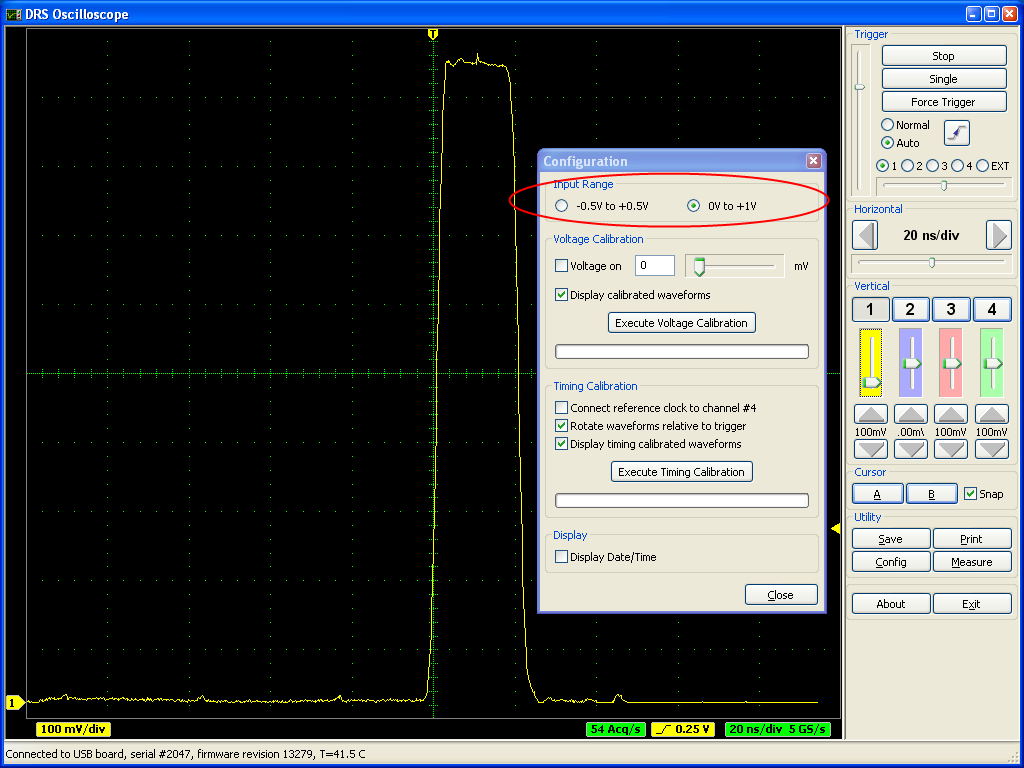
A board firmware update is not necessary for this. It was originally planned to have even a negative range -1V...0V, but this is not possible with the current board design. People who want to record negative pulses have to use an inverter to produce positive pulses. In a future version of the board it might be possible to include this functionality since this is determined by the analog front-end and not the DRS4 chip.
|
|
|
899
|
Mon Jun 12 14:22:04 2023 |
Stefan Ritt | Different sampling rates in multi-board configuration | No, that's unfortunately not possible.
Stefan
| Javier Caravaca wrote: |
|
Hello,
Is it possible to have different sampling rates in multi-board configuration? I tried using the scope application but I am unable to change the sampling rate independently.
Best,
Javier.
|
|
|
898
|
Fri Jun 9 04:11:40 2023 |
Javier Caravaca | Different sampling rates in multi-board configuration | Hello,
Is it possible to have different sampling rates in multi-board configuration? I tried using the scope application but I am unable to change the sampling rate independently.
Best,
Javier. |
|
897
|
Mon Feb 6 13:28:28 2023 |
Stefan Ritt | DRS4 installation via tar in ubuntu not working | I fixed the described error. Can you try the new version from https://bitbucket.org/ritt/drs4eb/commits/80b3af753ed32eb365725f0f3244a4109347c01b
| Sebastian Infante wrote: |
|
Hello i cant install any the last versions that i downloaded from the dropbox, i can untar the file called drs-5.0.6 and when i type "make" while inside the extracted folder that starts working properly till a point and i get an error, its worth mention that i installed wxWidgets and could make a simple hello world that worked properly in wxWidgets.
The error that i get is the next one:
inlined from ‘bool ResponseCalibration::ReadCalibrationV4(unsigned int)’ at src/DRS.cpp:7224:35:
/usr/include/x86_64-linux-gnu/bits/string_fortified.h:95:34: warning: ‘char* __builtin___strncpy_chk(char*, const char*, long unsigned int, long unsigned int)’ specified bound depends on the length of the source argument [-Wstringop-truncation]
95 | return __builtin___strncpy_chk (__dest, __src, __len,
| ~~~~~~~~~~~~~~~~~~~~~~~~^~~~~~~~~~~~~~~~~~~~~~
96 | __glibc_objsize (__dest));
| ~~~~~~~~~~~~~~~~~~~~~~~~~
src/DRS.cpp: In member function ‘bool ResponseCalibration::ReadCalibrationV4(unsigned int)’:
src/DRS.cpp:4767:11: note: length computed here
4767 | strncpy(calibrationDirectoryPath, fCalibDirectory, strlen(fCalibDirectory));
| ~~~~~~~^~~~~~~~~~~~~~~~~~~~~~~~~~~~~~~~~~~~~~~~~~~~~~~~~~~~~~~~~~~~~~~~~~~~
In file included from /usr/include/string.h:535,
from /usr/local/include/wx-3.3/wx/string.h:30,
from /usr/local/include/wx-3.3/wx/memory.h:15,
from /usr/local/include/wx-3.3/wx/object.h:19,
from /usr/local/include/wx-3.3/wx/wx.h:15,
from src/DRS.cpp:15:
In function ‘char* strncpy(char*, const char*, size_t)’,
inlined from ‘void DRSBoard::GetCalibrationDirectory(char*)’ at src/DRS.cpp:4767:11,
inlined from ‘bool ResponseCalibration::ReadCalibrationV3(unsigned int)’ at src/DRS.cpp:7066:35:
/usr/include/x86_64-linux-gnu/bits/string_fortified.h:95:34: warning: ‘char* __builtin___strncpy_chk(char*, const char*, long unsigned int, long unsigned int)’ specified bound depends on the length of the source argument [-Wstringop-truncation]
95 | return __builtin___strncpy_chk (__dest, __src, __len,
| ~~~~~~~~~~~~~~~~~~~~~~~~^~~~~~~~~~~~~~~~~~~~~~
96 | __glibc_objsize (__dest));
| ~~~~~~~~~~~~~~~~~~~~~~~~~
src/DRS.cpp: In member function ‘bool ResponseCalibration::ReadCalibrationV3(unsigned int)’:
src/DRS.cpp:4767:11: note: length computed here
4767 | strncpy(calibrationDirectoryPath, fCalibDirectory, strlen(fCalibDirectory));
| ~~~~~~~^~~~~~~~~~~~~~~~~~~~~~~~~~~~~~~~~~~~~~~~~~~~~~~~~~~~~~~~~~~~~~~~~~~~
g++ -g -O2 -Wall -Wuninitialized -fno-strict-aliasing -Iinclude -I/usr/local/include -DOS_LINUX -DHAVE_USB -DHAVE_LIBUSB10 -DUSE_DRS_MUTEX -I/usr/local/lib/wx/include/gtk3-unicode-3.3 -I/usr/local/include/wx-3.3 -D_FILE_OFFSET_BITS=64 -DWXUSINGDLL -D__WXGTK__ -pthread -c src/averager.cpp
g++ -g -O2 -Wall -Wuninitialized -fno-strict-aliasing -Iinclude -I/usr/local/include -DOS_LINUX -DHAVE_USB -DHAVE_LIBUSB10 -DUSE_DRS_MUTEX -I/usr/local/lib/wx/include/gtk3-unicode-3.3 -I/usr/local/include/wx-3.3 -D_FILE_OFFSET_BITS=64 -DWXUSINGDLL -D__WXGTK__ -pthread -c src/ConfigDialog.cpp
In file included from include/DRSOscInc.h:25,
from src/ConfigDialog.cpp:7:
include/DOFrame.h: In member function ‘bool DOFrame::GetRefclk()’:
include/DOFrame.h:111:46: error: ordered comparison of pointer with integer zero (‘bool*’ and ‘int’)
111 | bool GetRefclk() { return m_refClk > 0; }
| ~~~~~~~~~^~~
make: *** [Makefile:81: ConfigDialog.o] Error 1
|
|
|
896
|
Mon Oct 24 12:50:24 2022 |
Stefan Ritt | Channel Cascading Option in the 2048-bin | The board is delivered in one or the other mode and not meant to be changed by the user, since this requires very delicate soldering which is not easy. If you try anyhow, you loose the quarantee. You can send the board back to the manufacturer for the modification, but this costs quite some moeny.
Best regards,
Stefan
| Phan Van Chuan wrote: |
|
Dear Stefan,
We are using DRS4 evaluation board version 5.1 and firmware version 30000 (as the picture attached). Now, I am in need one channel with length 2048 bin. However, I can't find the resistors R99, ... ,R106 on the hardware of evaluation board; it seems my DRS4 evaluation board doesn't use 2048 bins per channel.
Our question is, can we repair this hardware to read 2048 bins/channel? if that is possible please let me know what to add on hardware/software of DRS4 evaluation.
Best regards.
Phan Van Chuan.
|
|
|
895
|
Sat Oct 22 13:24:20 2022 |
Phan Van Chuan | Channel Cascading Option in the 2048-bin | Dear Stefan,
We are using DRS4 evaluation board version 5.1 and firmware version 30000 (as the picture attached). Now, I am in need one channel with length 2048 bin. However, I can't find the resistors R99, ... ,R106 on the hardware of evaluation board; it seems my DRS4 evaluation board doesn't use 2048 bins per channel.
Our question is, can we repair this hardware to read 2048 bins/channel? if that is possible please let me know what to add on hardware/software of DRS4 evaluation.
Best regards.
Phan Van Chuan. |
| Attachment 1: DRS4V51.png
|

|
|
894
|
Mon Oct 17 16:29:37 2022 |
Sebastian Infante | DRS4 installation via tar in ubuntu not working | Hello i cant install any the last versions that i downloaded from the dropbox, i can untar the file called drs-5.0.6 and when i type "make" while inside the extracted folder that starts working properly till a point and i get an error, its worth mention that i installed wxWidgets and could make a simple hello world that worked properly in wxWidgets.
The error that i get is the next one:
inlined from ‘bool ResponseCalibration::ReadCalibrationV4(unsigned int)’ at src/DRS.cpp:7224:35:
/usr/include/x86_64-linux-gnu/bits/string_fortified.h:95:34: warning: ‘char* __builtin___strncpy_chk(char*, const char*, long unsigned int, long unsigned int)’ specified bound depends on the length of the source argument [-Wstringop-truncation]
95 | return __builtin___strncpy_chk (__dest, __src, __len,
| ~~~~~~~~~~~~~~~~~~~~~~~~^~~~~~~~~~~~~~~~~~~~~~
96 | __glibc_objsize (__dest));
| ~~~~~~~~~~~~~~~~~~~~~~~~~
src/DRS.cpp: In member function ‘bool ResponseCalibration::ReadCalibrationV4(unsigned int)’:
src/DRS.cpp:4767:11: note: length computed here
4767 | strncpy(calibrationDirectoryPath, fCalibDirectory, strlen(fCalibDirectory));
| ~~~~~~~^~~~~~~~~~~~~~~~~~~~~~~~~~~~~~~~~~~~~~~~~~~~~~~~~~~~~~~~~~~~~~~~~~~~
In file included from /usr/include/string.h:535,
from /usr/local/include/wx-3.3/wx/string.h:30,
from /usr/local/include/wx-3.3/wx/memory.h:15,
from /usr/local/include/wx-3.3/wx/object.h:19,
from /usr/local/include/wx-3.3/wx/wx.h:15,
from src/DRS.cpp:15:
In function ‘char* strncpy(char*, const char*, size_t)’,
inlined from ‘void DRSBoard::GetCalibrationDirectory(char*)’ at src/DRS.cpp:4767:11,
inlined from ‘bool ResponseCalibration::ReadCalibrationV3(unsigned int)’ at src/DRS.cpp:7066:35:
/usr/include/x86_64-linux-gnu/bits/string_fortified.h:95:34: warning: ‘char* __builtin___strncpy_chk(char*, const char*, long unsigned int, long unsigned int)’ specified bound depends on the length of the source argument [-Wstringop-truncation]
95 | return __builtin___strncpy_chk (__dest, __src, __len,
| ~~~~~~~~~~~~~~~~~~~~~~~~^~~~~~~~~~~~~~~~~~~~~~
96 | __glibc_objsize (__dest));
| ~~~~~~~~~~~~~~~~~~~~~~~~~
src/DRS.cpp: In member function ‘bool ResponseCalibration::ReadCalibrationV3(unsigned int)’:
src/DRS.cpp:4767:11: note: length computed here
4767 | strncpy(calibrationDirectoryPath, fCalibDirectory, strlen(fCalibDirectory));
| ~~~~~~~^~~~~~~~~~~~~~~~~~~~~~~~~~~~~~~~~~~~~~~~~~~~~~~~~~~~~~~~~~~~~~~~~~~~
g++ -g -O2 -Wall -Wuninitialized -fno-strict-aliasing -Iinclude -I/usr/local/include -DOS_LINUX -DHAVE_USB -DHAVE_LIBUSB10 -DUSE_DRS_MUTEX -I/usr/local/lib/wx/include/gtk3-unicode-3.3 -I/usr/local/include/wx-3.3 -D_FILE_OFFSET_BITS=64 -DWXUSINGDLL -D__WXGTK__ -pthread -c src/averager.cpp
g++ -g -O2 -Wall -Wuninitialized -fno-strict-aliasing -Iinclude -I/usr/local/include -DOS_LINUX -DHAVE_USB -DHAVE_LIBUSB10 -DUSE_DRS_MUTEX -I/usr/local/lib/wx/include/gtk3-unicode-3.3 -I/usr/local/include/wx-3.3 -D_FILE_OFFSET_BITS=64 -DWXUSINGDLL -D__WXGTK__ -pthread -c src/ConfigDialog.cpp
In file included from include/DRSOscInc.h:25,
from src/ConfigDialog.cpp:7:
include/DOFrame.h: In member function ‘bool DOFrame::GetRefclk()’:
include/DOFrame.h:111:46: error: ordered comparison of pointer with integer zero (‘bool*’ and ‘int’)
111 | bool GetRefclk() { return m_refClk > 0; }
| ~~~~~~~~~^~~
make: *** [Makefile:81: ConfigDialog.o] Error 1
|
|
893
|
Tue Sep 27 15:20:55 2022 |
Stefan Ritt | Required Firmware for DRS4 Evaluation Board Version 2.0 | Sorry, got the wrong link. Here the right one: https://www.dropbox.com/sh/clqo7ekr0ysbrip/AACoWJzrQAbf3WiBJHG89bGGa?dl=0
If you untar the archive, you will find a "firmware" subdirectory with all VHDL code.
Stefan
| Kunal Shinde wrote: |
|
I checked the link you provided but it seems that the link doesnt exist please send me valid one.
Regards,
Kunal
| Stefan Ritt wrote: |
|
You find each software version at the usual download location at
https://www.dropbox.com/home/drs/drs4/distribution/Download/Linux
The one you need is probably drs-2.1.3.tar.gz which was the last version for the 2.0 board which is now more than 10 years old.
Best,
Stefan
| Kunal Shinde wrote: |
|
Hi, I am working on an old DRS4 board Version "2.0" with firmware revision "13191", I was unable to find this specific firmware source files ("VHDL source code"), please help me where could I find this or send me the required.
Regards,
Kunal
|
|
|
|
|
892
|
Tue Sep 27 10:52:41 2022 |
Kunal Shinde | Required Firmware for DRS4 Evaluation Board Version 2.0 | I checked the link you provided but it seems that the link doesnt exist please send me valid one.
Regards,
Kunal
| Stefan Ritt wrote: |
|
You find each software version at the usual download location at
https://www.dropbox.com/home/drs/drs4/distribution/Download/Linux
The one you need is probably drs-2.1.3.tar.gz which was the last version for the 2.0 board which is now more than 10 years old.
Best,
Stefan
| Kunal Shinde wrote: |
|
Hi, I am working on an old DRS4 board Version "2.0" with firmware revision "13191", I was unable to find this specific firmware source files ("VHDL source code"), please help me where could I find this or send me the required.
Regards,
Kunal
|
|
|
|
891
|
Tue Sep 27 10:37:11 2022 |
Stefan Ritt | Required Firmware for DRS4 Evaluation Board Version 2.0 | You find each software version at the usual download location at
https://www.dropbox.com/home/drs/drs4/distribution/Download/Linux
The one you need is probably drs-2.1.3.tar.gz which was the last version for the 2.0 board which is now more than 10 years old.
Best,
Stefan
| Kunal Shinde wrote: |
|
Hi, I am working on an old DRS4 board Version "2.0" with firmware revision "13191", I was unable to find this specific firmware source files ("VHDL source code"), please help me where could I find this or send me the required.
Regards,
Kunal
|
|
|
890
|
Tue Sep 27 10:17:58 2022 |
Kunal Shinde | Required Firmware for DRS4 Evaluation Board Version 2.0 | Hi, I am working on an old DRS4 board Version "2.0" with firmware revision "13191", I was unable to find this specific firmware source files ("VHDL source code"), please help me where could I find this or send me the required.
Regards,
Kunal |
|
889
|
Wed Sep 7 10:13:41 2022 |
Prajjalak Chattopadhyay | Register status after reset | What are the default register statuses after DRS4 gets reset? |
|
888
|
Fri Jul 29 17:23:43 2022 |
Stefan Ritt | Spikes/noise sensitive to clock settings? | Look at the DRS4 data sheet, Figure 12. You see there the rising SRCLK pulse which outputs the next analog value. You also see tSAMP which describes the sampling piont (strobe or clock sent to your ADC). The value of tSAMP must be such that the values is sampled at the point where it flattens out, just 2-3 ns BEFORE the next analog sample is clocked out, as written in the text. So you have to phase shift your clock going to SRCLK and the one going to your ADC against each other. This needs adjustment at the ns level, so you need a PLL with fine-valued taps, so you can shift it in fractions of a ns. What you see is that you sample at the BEGINNING of a new value to be output to the chip. Please also note that most ADCs have an internal delay of their clock (usually called 'aperture') which has to be taken into account. So if your SRCLK and your ADC clock come at the same time (not phase shifted), it might happen that the ADC internal aperture delay caues it to sample the analog signal at the BEGINNING of the new value.
Hope this is clearer now.
Best regards,
Stefan |
|
887
|
Fri Jul 29 14:09:35 2022 |
Stefan Ritt | Increase event rate, use ROI mode, and install sw from source in Mac | The firmware from the website always reads 1024 bins. You have to modify it to stop before that, like reading only 128 samples or so. For compiling under MacOSX, this should work, since I do it myself.
Regards,
Stefan
| Jingyu Zhang wrote: |
|
Dear experts,
We are trying to increase the event rate of the DRS4. We looked into the ROI but couldn’t figure out how to run in ROI mode. We are wondering if there is pre-existing firmware for this? We also tried to download and build the software from source on MacOS 12.4 but we were not successful. Can you kindly help us with these?
Best regards,
Jingyu
|
|
|
886
|
Tue Jul 19 02:35:04 2022 |
Jingyu Zhang | Increase event rate, use ROI mode, and install sw from source in Mac | Dear experts,
We are trying to increase the event rate of the DRS4. We looked into the ROI but couldn’t figure out how to run in ROI mode. We are wondering if there is pre-existing firmware for this? We also tried to download and build the software from source on MacOS 12.4 but we were not successful. Can you kindly help us with these?
Best regards,
Jingyu |
|
885
|
Fri Jun 24 09:57:36 2022 |
LynseyShun | Spikes/noise sensitive to clock settings? | Hello, I now have periodic spikes in CH0 and CH1 output. How can I eliminate these spikes? I'm sorry I didn't understand your elimination method. Please explain the method in detail. Thank you very much
| Stefan Ritt wrote: |
|
elog:824
| Sean Quinn wrote: |
|
Dear DRS4 team,
I'm trying to troubleshoot some odd spike behavior. If I run the ADC and SR CLK at 16 MHz (behavior also seen at 33 MHz) we get very noisy data (post-calibration) with periodic spikes.
In the below plot
- CH0 & CH1 are muon pulses from a scintillator + SiPM detector
- CH8 is a 25 MHz sinewave (in phase with all generated board clocks)
- Transparent mode = ON
- ROI = OFF, "full readout mode", first sample = cell 0
- DRS REFCLK = 1 MHz (2 GS/s)
- ADC & SR CLK = 16 MHz, 0 deg. offset
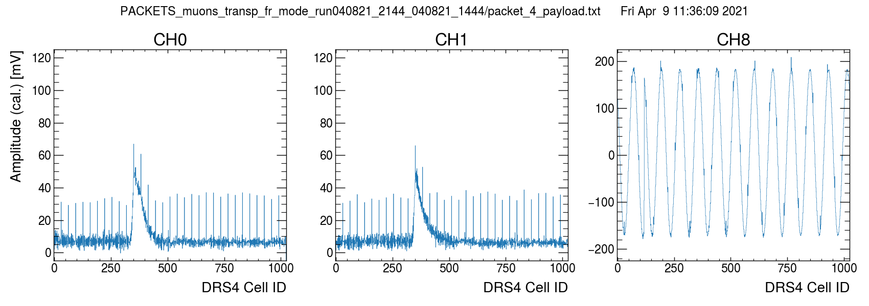
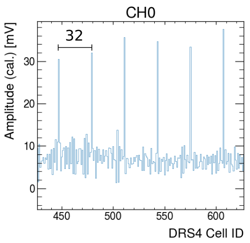
After I modify some clock settings, things seem to improve dramatically, and the spike behavior changes
- ADC and SR CLK = 15 MHz, 0 deg. offset
- Transparent mode = ON
- ROI = ON (just for testing purposes)
- Add 1.064 ns skew to DRS REF CLK
- NOTE: Unfortunately due to a design mishap, the ADC and FPGA clock use a phase-locked output pair on our clock synthesis chip, so we cannot fine-tune the skew for it.
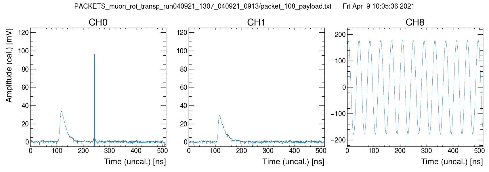
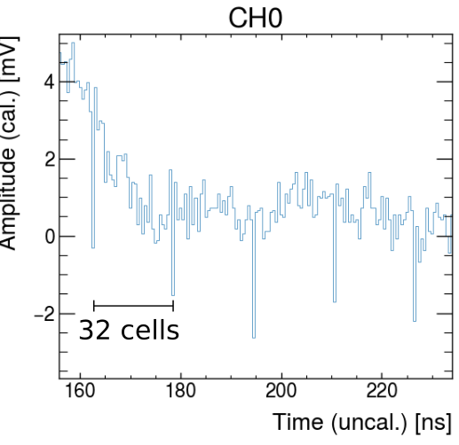
Observed differences
- Spike polarity seems inverted
- Spikes limited to smaller number of cells now?
- Spike amplitude reduced
- Overall baseline variance seems better
- New large positive spike artifact on CH0 that seems inverted on CH1
- CH8 seems unaffected by large spikes?
Artifacts seem related to clock configuration, but I am sort of in the dark on what might be happening from a first-principles point of view. Any tips?
Warm regards,
Sean
|
|
|
|
884
|
Thu Jun 16 05:31:25 2022 |
LynseyShun | | Thank you very much for your help!
| Stefan Ritt wrote: |
|
A3-A0 = 1001 should be all you need to activate OUT0-OUT7. It works in our designs. Maybe double check the address lines with an oscilloscope.
Stefan
| LynseyShun wrote: |
|
Hello, I am Lynsey. now I set A3-A0 to 1001 in ROI mode, but only OUT0 has output, and the other seven channels(OUT1-OUT7) do not output corresponding waveforms.
In ROI mode, can OUT0-OUT7 output sampled waveforms at the same time?
thank you very much
|
|
|
|
883
|
Tue Apr 12 10:49:27 2022 |
Stefan Ritt | | A3-A0 = 1001 should be all you need to activate OUT0-OUT7. It works in our designs. Maybe double check the address lines with an oscilloscope.
Stefan
| LynseyShun wrote: |
|
Hello, I am Lynsey. now I set A3-A0 to 1001 in ROI mode, but only OUT0 has output, and the other seven channels(OUT1-OUT7) do not output corresponding waveforms.
In ROI mode, can OUT0-OUT7 output sampled waveforms at the same time?
thank you very much
|
|
|
882
|
Tue Apr 12 10:40:36 2022 |
LynseyShun | | Hello, I am Lynsey. now I set A3-A0 to 1001 in ROI mode, but only OUT0 has output, and the other seven channels(OUT1-OUT7) do not output corresponding waveforms.
In ROI mode, can OUT0-OUT7 output sampled waveforms at the same time?
thank you very much |
|
881
|
Tue Mar 15 13:07:50 2022 |
Matias Senger | Time calibration and the C++ API | Thanks for your help. If I look into the app the behavior for the 4 channels is exactly as you show:


Now, when I sample with my code something strange happens, two of the channels are fine and the other two are wrong:

This is a surprise to me because I acquire the 4 channels in the same way within a `for` loop. To get the time data I use `DRSBoard::GetTime` with the `tcalibrated` argument set to `true`. Is there any aditional step to use the calibration?
Best,
Matias.
| Stefan Ritt wrote: |
|
Looks like you have the some time calibration, not sure if it's the correct one. Sample the sine wave from the calibration clock, once with and once without the timing calibration, then you will see if all points lie on a smooth line. Left: without timing calibration, right: with proper timing calibration:
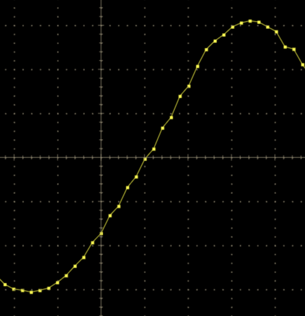 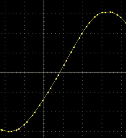
If your points do not lie on a smooth line, you might habe a problem such as the wrong channel for calibration, an offset of 1 in the index of the time array or some other software bug. Measure the same signal with the DRSOsc application and then your code. If the results differ, you have a software problem on your side.
Stefan
|
|
|
880
|
Mon Mar 14 08:59:51 2022 |
Stefan Ritt | Time calibration and the C++ API | Looks like you have the some time calibration, not sure if it's the correct one. Sample the sine wave from the calibration clock, once with and once without the timing calibration, then you will see if all points lie on a smooth line. Left: without timing calibration, right: with proper timing calibration:
If your points do not lie on a smooth line, you might habe a problem such as the wrong channel for calibration, an offset of 1 in the index of the time array or some other software bug. Measure the same signal with the DRSOsc application and then your code. If the results differ, you have a software problem on your side.
Stefan
|
|
879
|
Sat Mar 12 16:52:36 2022 |
Matias Senger | Time calibration and the C++ API | Dear Stefan,
For the time of each bin I am using the values returend by `GetTime` without any assumption by my side. I did not notice before that the sampling time is not uniform, but I see that this is already happening. This is an example plot from one of the signals I processed:

The bin at 65.5 ns and the next one are closer than their neighbors. So this seems to indicate that the time calibration is being taken into account when I acquire the time bins using `GetTime`, is this correct?
To obtain the final time resolution I am using the constant fraction discriminator method and the signals are linearly interpolated to obtain the time at each percentage value, as seen in the plot. I have already measured time resolutions in the 5-100 ps range with exactly the same setup but using the LeCroy oscilloscope, which I am using just for data acquisition, and my software for offline analysis as shown in the plot above. Now what I am trying to do is to replace the LeCroy by the DRS4 Evaluation Board basically, so I can use the oscilloscope in a different setup.
Best,
Matias.
| Stefan Ritt wrote: |
|
DRSBoard::GetTime is declared in DRS.h line 720.
If you want to measure timing down to ps, you need some basic knowledge, especially about signal-to-noise and risetime. This cannot be taught in a few sentenses, needs a full lecture. As a starting point please read that papat:
https://arxiv.org/abs/1405.4975
then you will understand why you measure different resolutions with different peak heights (and different rise times).
Concerning the DRS4 measurement, please be aware that the sampling poings are not equidistant, like not every 200ps for GSPS. They vary bin by bin significantly, from 50ps to 300ps. So you alway have to analyse the X/Y points as an array, not just the Y values assuming deltaX of 200ps. Probably you forgot that. Then, you have to interpolate between bins to find the crossing over your threshold. Linear interpolation is already good, spline interpolation even better. Deep inside Measurement.cpp of the drsosc program you find in the source code:
t1 = (thr*(x1[i]-x1[i-1])+x1[i-1]*y1[i]-x1[i]*y1[i-1])/(y1[i]-y1[i-1]);
which is the linear interpolation (thr is the threshold). You have to use (and understand!) similar code.
Best,
Stefan
| Matias Senger wrote: |
|
I am using the V5 board at a fixed sampling frequency. With the `drsosc` app I have executed the time calibration at 5 GS/s (actually 5.12 GS/s). This is how my setup looks like in the app:

Now I want to replicate this using the C++ API (not the positive width measurement shown, the signal sampling only). I am seting the sampling frequency to 5 GS/s, as I do in the `drsosc` app. Then I get the time information using the `DRSBoard::GetTime(unsigned int chipIndex, int channelIndex, int tc, float *time)` function (which I don't find defined either in `DRS.h` or `DRS.cpp` but somehow it works). How can I know if these times that I get here are being corrected with the time calibration? If so, should I expect the time resolution to be < 3 ps? Are these 3 ps accumulative, such that in the end I end up having a contribution from the evaluation board of 3 ps × 5 Gs/s × 100 ns where 100 ns is the time difference between my two pulses? (This does not seem to be the case because if so I would expect the jitter to be ~ 1 ns, and we see that the "Pos Width" measurement is ~ 0.1 ns std.)
Why am I asking? I want to measure the jitter between the two falling edges. This cannot be done easily with the `drsosc` app I think, so I am acquiring the data and doing this offline. I have done this measurement in the past using a LeCroy WaveRunner oscilloscope with 20 GS/s and 4 GHz bandwidth (offline, same code) and I have seen it vary from ~5 ps → 30 ps when I vary a voltage that I can control. Now if I calculate this time fluctuation using the data acquired with the V5 evaluation board I get a value ~100 ps and independent of this voltage, which leads me to conclude that the limiting factor is being the evaluation board itself. So now I am wondering if I have reached its limit, or if there is some setting that can still improve this result.
Thanks!
|
|
|
|
878
|
Sat Mar 12 10:13:24 2022 |
Stefan Ritt | Time calibration and the C++ API | DRSBoard::GetTime is declared in DRS.h line 720.
If you want to measure timing down to ps, you need some basic knowledge, especially about signal-to-noise and risetime. This cannot be taught in a few sentenses, needs a full lecture. As a starting point please read that papat:
https://arxiv.org/abs/1405.4975
then you will understand why you measure different resolutions with different peak heights (and different rise times).
Concerning the DRS4 measurement, please be aware that the sampling poings are not equidistant, like not every 200ps for GSPS. They vary bin by bin significantly, from 50ps to 300ps. So you alway have to analyse the X/Y points as an array, not just the Y values assuming deltaX of 200ps. Probably you forgot that. Then, you have to interpolate between bins to find the crossing over your threshold. Linear interpolation is already good, spline interpolation even better. Deep inside Measurement.cpp of the drsosc program you find in the source code:
t1 = (thr*(x1[i]-x1[i-1])+x1[i-1]*y1[i]-x1[i]*y1[i-1])/(y1[i]-y1[i-1]);
which is the linear interpolation (thr is the threshold). You have to use (and understand!) similar code.
Best,
Stefan
| Matias Senger wrote: |
|
I am using the V5 board at a fixed sampling frequency. With the `drsosc` app I have executed the time calibration at 5 GS/s (actually 5.12 GS/s). This is how my setup looks like in the app:
Now I want to replicate this using the C++ API (not the positive width measurement shown, the signal sampling only). I am seting the sampling frequency to 5 GS/s, as I do in the `drsosc` app. Then I get the time information using the `DRSBoard::GetTime(unsigned int chipIndex, int channelIndex, int tc, float *time)` function (which I don't find defined either in `DRS.h` or `DRS.cpp` but somehow it works). How can I know if these times that I get here are being corrected with the time calibration? If so, should I expect the time resolution to be < 3 ps? Are these 3 ps accumulative, such that in the end I end up having a contribution from the evaluation board of 3 ps × 5 Gs/s × 100 ns where 100 ns is the time difference between my two pulses? (This does not seem to be the case because if so I would expect the jitter to be ~ 1 ns, and we see that the "Pos Width" measurement is ~ 0.1 ns std.)
Why am I asking? I want to measure the jitter between the two falling edges. This cannot be done easily with the `drsosc` app I think, so I am acquiring the data and doing this offline. I have done this measurement in the past using a LeCroy WaveRunner oscilloscope with 20 GS/s and 4 GHz bandwidth (offline, same code) and I have seen it vary from ~5 ps → 30 ps when I vary a voltage that I can control. Now if I calculate this time fluctuation using the data acquired with the V5 evaluation board I get a value ~100 ps and independent of this voltage, which leads me to conclude that the limiting factor is being the evaluation board itself. So now I am wondering if I have reached its limit, or if there is some setting that can still improve this result.
Thanks!
|
|
|
877
|
Fri Mar 11 17:26:15 2022 |
Matias Senger | Time calibration and the C++ API | I am using the V5 board at a fixed sampling frequency. With the `drsosc` app I have executed the time calibration at 5 GS/s (actually 5.12 GS/s). This is how my setup looks like in the app:
Now I want to replicate this using the C++ API (not the positive width measurement shown, the signal sampling only). I am seting the sampling frequency to 5 GS/s, as I do in the `drsosc` app. Then I get the time information using the `DRSBoard::GetTime(unsigned int chipIndex, int channelIndex, int tc, float *time)` function (which I don't find defined either in `DRS.h` or `DRS.cpp` but somehow it works). How can I know if these times that I get here are being corrected with the time calibration? If so, should I expect the time resolution to be < 3 ps? Are these 3 ps accumulative, such that in the end I end up having a contribution from the evaluation board of 3 ps × 5 Gs/s × 100 ns where 100 ns is the time difference between my two pulses? (This does not seem to be the case because if so I would expect the jitter to be ~ 1 ns, and we see that the "Pos Width" measurement is ~ 0.1 ns std.)
Why am I asking? I want to measure the jitter between the two falling edges. This cannot be done easily with the `drsosc` app I think, so I am acquiring the data and doing this offline. I have done this measurement in the past using a LeCroy WaveRunner oscilloscope with 20 GS/s and 4 GHz bandwidth (offline, same code) and I have seen it vary from ~5 ps → 30 ps when I vary a voltage that I can control. Now if I calculate this time fluctuation using the data acquired with the V5 evaluation board I get a value ~100 ps and independent of this voltage, which leads me to conclude that the limiting factor is being the evaluation board itself. So now I am wondering if I have reached its limit, or if there is some setting that can still improve this result.
Thanks! |
|
876
|
Tue Mar 8 12:20:00 2022 |
Matias Senger | Why does not trigger at higher sampling frequencies? | Sorry for the spam. Just want to let you know that I was able to solve the problem, it was all due to a `float` being casted as `int` in the Python binding. Now it works like a charm.
| Matias Senger wrote: |
|
I have seen in the app that the trigger source buttons do something different than the "or" and "transparent trigger" buttons:

If I enable the setup from the right, i.e. OR in CH4 and "Enable Transparent Trigger" the app stops triggering. This is the configuration that seems to be applied in the `drs_exam.cpp` code if I am not mistaken. For some reason in that code it still triggers (I have modified the code to trigger on CH4 instead of CH1 and the trigger level, polarity, etc.).
What does the button in the left actually do? The circular checkbox with the "4" I mean. This is the trigger configuration I want to get in the C++ code.
I also don't know what the function `DRSBoard::EnableTrigger` does, what is the meaning of `flag1` and `flag2`? In my code there is a call to this function which I copied from the example.
| Stefan Ritt wrote: |
|
Unfortunately I have not idea what the problem could be. In principle the trigger should be independent of the sampling speed, since the trigger is only made with a discriminator and a flip-flop. The hardware must be ok since you see the trigger with the oscillocope app. All you can do is to go through the sorce code of the oscilloscope app, especially drsosc/Osic.cpp::ScanBoards(), SetTriggerLevel(), SetTriggerPolariy() etc. to make sure you do the same calls as the oscilloscope app.
Stefan
|
|
|
|
875
|
Tue Mar 8 00:25:56 2022 |
Matias Senger | Why does not trigger at higher sampling frequencies? | I have seen in the app that the trigger source buttons do something different than the "or" and "transparent trigger" buttons:
If I enable the setup from the right, i.e. OR in CH4 and "Enable Transparent Trigger" the app stops triggering. This is the configuration that seems to be applied in the `drs_exam.cpp` code if I am not mistaken. For some reason in that code it still triggers (I have modified the code to trigger on CH4 instead of CH1 and the trigger level, polarity, etc.).
What does the button in the left actually do? The circular checkbox with the "4" I mean. This is the trigger configuration I want to get in the C++ code.
I also don't know what the function `DRSBoard::EnableTrigger` does, what is the meaning of `flag1` and `flag2`? In my code there is a call to this function which I copied from the example.
| Stefan Ritt wrote: |
|
Unfortunately I have not idea what the problem could be. In principle the trigger should be independent of the sampling speed, since the trigger is only made with a discriminator and a flip-flop. The hardware must be ok since you see the trigger with the oscillocope app. All you can do is to go through the sorce code of the oscilloscope app, especially drsosc/Osic.cpp::ScanBoards(), SetTriggerLevel(), SetTriggerPolariy() etc. to make sure you do the same calls as the oscilloscope app.
Stefan
|
|
|
874
|
Mon Mar 7 16:37:54 2022 |
Stefan Ritt | Scaler issue to evaluate live time | I tried your measurement with the DRSOscilloscope app (see below), and I measure a constant difference of 10 Hz among the whole range of 100 Hz to 3 kHz.
So I don't know what's wrong on your side. Did you try with the oscilloscope app as well? Have you checked your pulse generator? The evaluation board time reference is a quartz with an accuracy of 10^-5, so no way one can get there a difference you see.
Stefan
| Keita Mizukoshi wrote: |
|
Thank you very much for your explanation.
I would like to show you a pulse example ('black line is the threshold).
Still, pulse generator rate and DRS4 rate are a bit different more than 10 Hz.
| Stefan Ritt wrote: |
|
The scalers are read out 10x per seconds, so they have an accuracy of 10 Hz. I tried a 50 Hz pulser, and measured 40 Hz, I tried 52 Hz and measured 50 Hz. This is about what you can expect.
The scaler rate is measured after the discriminator of the trigger, so the trigger level also affects the scaler reading. If you have a 100 mV pulse and your threshold is 200 mV, your scaler rate drops to zero. That can be seen best with the DRSOsc and sliding the trigger value. If you have a 50 Hz pulse with narrow (< us) pulses, things are fine. But if you use a 50 Hz square wave, then you get distorted signals due to the AC coupling which can also be confusing. See for example here: https://www.daqarta.com/dw_gg0o.htm
| Keita Mizukoshi wrote: |
|
Hi. I'm trying to evaluate livetime of the evaluation board with the hardware scaler. I'm facing a strange issue.
I took the rate with the function, DRS->GetScaler(int channel).
I guess that channels 0--3 mean the rate for the channel, and channel 4 means the counter of the trigger.
I took the 1,000 pulses generated by a pulse generator with 50 Hz.
The scaler values are ~ 39.83, not 50.
The timestamp difference between the initial event and the final event is 19.98 seconds.
1000/19.98 ~ 50, thus, the evaluation board took the pulses with enough livetime.
Can we believe the scaler value for the livetime evaluation?
|
|
|
|
| Attachment 1: Screenshot_2022-03-07_at_16.37.32_.png
|

|
| Attachment 2: Screenshot_2022-03-07_at_16.35.44_.png
|

|
|
873
|
Mon Mar 7 13:38:03 2022 |
Radoslaw Marcinkowski | Problems with DRS4 Evaluation Board after Windows 10 upgrade - share of experiences | Dear DRS4 Users,
I would like to share my expireinces with using of DRS4 Evaluation Board software (oscilloscope) after upgrade of Windows 10.
I had Windows 10 (Enterprise) in version from ~2016. It was working fine with DRS4 Scope software. Due to the company policy, Windows was upgraded to the newer version (2019). Since this time the board was not recognized any more as DRS4 Evaluation Board, both by Windows and DRS4 Scope standard software. Changing USB sockets did not help at all. I installed once more time Zadig USB driver (suggested by https://www.psi.ch/en/drs/software-download), no Admistrator rights were needed. It took long time, about 10 minutes or more, it suggested restart in the meantime, and finally noticed that ... installation failed! Even that, DRS4 software started to recognize the board without the problem even without reboot. Let me notice that all users on this machine can use the DRS4 software even if installation was done by non-administrator user.
Regards,
Radek |
|
872
|
Mon Mar 7 08:45:32 2022 |
Stefan Ritt | Why does not trigger at higher sampling frequencies? | Unfortunately I have not idea what the problem could be. In principle the trigger should be independent of the sampling speed, since the trigger is only made with a discriminator and a flip-flop. The hardware must be ok since you see the trigger with the oscillocope app. All you can do is to go through the sorce code of the oscilloscope app, especially drsosc/Osic.cpp::ScanBoards(), SetTriggerLevel(), SetTriggerPolariy() etc. to make sure you do the same calls as the oscilloscope app.
Stefan |
|
871
|
Sun Mar 6 17:54:47 2022 |
Matias Senger | Why does not trigger at higher sampling frequencies? | I have connected 3 signals to the DRS4 Evaluation Board V5 which look like this in the drsosc app:

Note that here I am sampling at 5 GS/s. Using this app everything works perfect.
Now I want to repeat this using the C++ API (which I am actually wrapping to use within Python, see here if interested https://github.com/SengerM/pydrs ) but can only make this to work at lower sampling frequencies up to 3.9 GS/s. This is how I am configuring the board followint the `drs_exam.cpp` file:
```python
board.set_sampling_frequency(Hz=SAMPLING_FREQ)
board.set_transparent_mode('on')
board.set_input_range(center=0)
board.enable_trigger(True,False) # Don't know what this line does, it was in the example `drs_exam.cpp`.
board.set_trigger_source('ch4')
board.set_trigger_level(volts=-.1)
board.set_trigger_polarity(edge='falling')
board.set_trigger_delay(seconds=TRIGGER_DELAY)
```
The full code is here https://github.com/SengerM/pydrs/blob/master/tests/test_drs.py but anyway, my previous snippet can be considered as pseudo-code and if more details needed I can provide.
This is what I get as I increase the sampling frequency:


Up to 3.95 GS/s it works perfectly. At >= 4 GS/s it just never triggers. A few times I was able to make this work at 4 and 5 GS/s playing with the trigger delay, but this seemed to be some kind of random luck because I was not able to replicate it even with the same values.
Any help is appreciated.
Best,
Matías. |
|
870
|
Fri Mar 4 03:55:33 2022 |
Keita Mizukoshi | Scaler issue to evaluate live time | Thank you very much for your explanation.
I would like to show you a pulse example ('black line is the threshold).
Still, pulse generator rate and DRS4 rate are a bit different more than 10 Hz.
| Stefan Ritt wrote: |
|
The scalers are read out 10x per seconds, so they have an accuracy of 10 Hz. I tried a 50 Hz pulser, and measured 40 Hz, I tried 52 Hz and measured 50 Hz. This is about what you can expect.
The scaler rate is measured after the discriminator of the trigger, so the trigger level also affects the scaler reading. If you have a 100 mV pulse and your threshold is 200 mV, your scaler rate drops to zero. That can be seen best with the DRSOsc and sliding the trigger value. If you have a 50 Hz pulse with narrow (< us) pulses, things are fine. But if you use a 50 Hz square wave, then you get distorted signals due to the AC coupling which can also be confusing. See for example here: https://www.daqarta.com/dw_gg0o.htm
| Keita Mizukoshi wrote: |
|
Hi. I'm trying to evaluate livetime of the evaluation board with the hardware scaler. I'm facing a strange issue.
I took the rate with the function, DRS->GetScaler(int channel).
I guess that channels 0--3 mean the rate for the channel, and channel 4 means the counter of the trigger.
I took the 1,000 pulses generated by a pulse generator with 50 Hz.
The scaler values are ~ 39.83, not 50.
The timestamp difference between the initial event and the final event is 19.98 seconds.
1000/19.98 ~ 50, thus, the evaluation board took the pulses with enough livetime.
Can we believe the scaler value for the livetime evaluation?
|
|
|
| Attachment 1: pulse_example.png
|

|
| Attachment 2: rate.png
|

|
|
869
|
Thu Mar 3 16:14:16 2022 |
Stefan Ritt | Scaler issue to evaluate live time | The scalers are read out 10x per seconds, so they have an accuracy of 10 Hz. I tried a 50 Hz pulser, and measured 40 Hz, I tried 52 Hz and measured 50 Hz. This is about what you can expect.
The scaler rate is measured after the discriminator of the trigger, so the trigger level also affects the scaler reading. If you have a 100 mV pulse and your threshold is 200 mV, your scaler rate drops to zero. That can be seen best with the DRSOsc and sliding the trigger value. If you have a 50 Hz pulse with narrow (< us) pulses, things are fine. But if you use a 50 Hz square wave, then you get distorted signals due to the AC coupling which can also be confusing. See for example here: https://www.daqarta.com/dw_gg0o.htm
| Keita Mizukoshi wrote: |
|
Hi. I'm trying to evaluate livetime of the evaluation board with the hardware scaler. I'm facing a strange issue.
I took the rate with the function, DRS->GetScaler(int channel).
I guess that channels 0--3 mean the rate for the channel, and channel 4 means the counter of the trigger.
I took the 1,000 pulses generated by a pulse generator with 50 Hz.
The scaler values are ~ 39.83, not 50.
The timestamp difference between the initial event and the final event is 19.98 seconds.
1000/19.98 ~ 50, thus, the evaluation board took the pulses with enough livetime.
Can we believe the scaler value for the livetime evaluation?
|
|
|
868
|
Thu Mar 3 13:47:26 2022 |
Stefan Ritt | How to convert samples to volt? | The 'drscl' tool is more for experts, normal users are advised to use the DRSOsc oscilloscope.
The board has to be calibrated for a given sampling speed before calibrated data can be read out. Do that with the "calib" command, specifying 5 for the sampling rate, 0 for the range (which is the middle between -0.5 and +0.5) and 1 for 1024 mode. If you then do "start", "stop", "read 0 1" you get calibrated data in mV.
Stefan
| Matias Senger wrote: |
|
I am using the `drscl` app. My prior experience is practically zero, sorry if this is a very naive question. When I read using `read 0 1` (channel 0, with calibration) I get this:
```
Calibration not valid for board #2946
10 3 7 4 10 8 14 5 5 9 3 4 9 8 9 4
3 3 12 5 5 13 3 8 1 5 0 4 8 6 6 3
...etc...
```
Why does it says that the calibration is not valid? How am I supposed to go from integers to volts?
If I run the `info` command I get this:
```
==============================
Mezz. Board index: 0
DRS type: DRS4
Board type: 9
Serial number: 2946
Firmware revision: 30000
Temperature: 43.4 C
Input range: -0.5V...0.5V
Calibrated range: -0.5V...0.5V
Calibrated frequency: 0.000 GHz
Status reg.: 0000009A
Control reg.: 00000000
DMODE circular
Trigger bus: 00000000
Frequency: 1.007 GHz
```
|
|
|
867
|
Wed Mar 2 17:25:10 2022 |
Matias Senger | How to convert samples to volt? | I am using the `drscl` app. My prior experience is practically zero, sorry if this is a very naive question. When I read using `read 0 1` (channel 0, with calibration) I get this:
```
Calibration not valid for board #2946
10 3 7 4 10 8 14 5 5 9 3 4 9 8 9 4
3 3 12 5 5 13 3 8 1 5 0 4 8 6 6 3
...etc...
```
Why does it says that the calibration is not valid? How am I supposed to go from integers to volts?
If I run the `info` command I get this:
```
==============================
Mezz. Board index: 0
DRS type: DRS4
Board type: 9
Serial number: 2946
Firmware revision: 30000
Temperature: 43.4 C
Input range: -0.5V...0.5V
Calibrated range: -0.5V...0.5V
Calibrated frequency: 0.000 GHz
Status reg.: 0000009A
Control reg.: 00000000
DMODE circular
Trigger bus: 00000000
Frequency: 1.007 GHz
``` |
|
866
|
Tue Mar 1 19:03:37 2022 |
Keita Mizukoshi | Scaler issue to evaluate live time | Hi. I'm trying to evaluate livetime of the evaluation board with the hardware scaler. I'm facing a strange issue.
I took the rate with the function, DRS->GetScaler(int channel).
I guess that channels 0--3 mean the rate for the channel, and channel 4 means the counter of the trigger.
I took the 1,000 pulses generated by a pulse generator with 50 Hz.
The scaler values are ~ 39.83, not 50.
The timestamp difference between the initial event and the final event is 19.98 seconds.
1000/19.98 ~ 50, thus, the evaluation board took the pulses with enough livetime.
Can we believe the scaler value for the livetime evaluation? |
|
865
|
Wed Feb 16 14:06:45 2022 |
Dmitry Hits | Sliders missing in drsosc | Hi everyone,
Did anyone have a "missing sliders problem" in GUI (see attachment) accompanied by the following message in the terminal.
(drsosc:4611): Gtk-WARNING **: 14:05:11.249: Negative content width -4 (allocation 20, extents 12x12) while allocating gadget (node scale, owner GtkScale)
(drsosc:4611): Gtk-WARNING **: 14:05:11.249: Negative content width -2 (allocation 0, extents 1x1) while allocating gadget (node trough, owner GtkScale)
If yes, how did you solve it?
All ideas are appreciated!
Cheers,
Dmitry
|
| Attachment 1: Screen_Shot_2022-02-14_at_14.17.30.png
|

|
|
864
|
Tue Feb 15 12:02:29 2022 |
Stefan Ritt | Cannot trigger on pulses, have to trigger on undershoot | The trigger comparator is a ADCMP601 unit which requires a minimum pulse width of 3-4 ns. I see that your pulses are only 1-2 ns wide. You have to make your pulses wider in order to trigger on them.
Stefan |
|
863
|
Tue Feb 15 11:59:22 2022 |
Alex Myczko | apt install drs4eb | drs4b is now officially on these distributions:
https://repology.org/project/drs4eb/versions
enjoy |
|
862
|
Sat Feb 12 13:06:56 2022 |
Matias Senger | Cannot trigger on pulses, have to trigger on undershoot | I am using the DRS4 board trying to measure pulses produced by an LGAD. I have no prior experience with this board, have just installed the `drsosc` application and am exploring. I am experiencing some strange trigger behavior. Consider the following screenshot:

Here nothing is strange, the board is triggering on the undershoot and it is working fine, I can trigger on rising/falling edge, different levels, etc.
Now, the strange thing is that if I pull the trigger up to trigger on the pulse itself it stops triggering:

I have tried many different setups for the trigger (rising, falling edge, different levels, etc) and nothing works. In the undershoot, everything works.
I have tried with the internal test signal and it works fine:

What could be the problem?
I have run the voltage and time calibrations as suggested in the manual. |
|
861
|
Wed Jan 26 06:44:11 2022 |
student_riku | I want to know about the readout | Dear Stefan
Thanks a lot.
I solved it.
| Stefan Ritt wrote: |
| student_riku wrote: |
|
Am I right in thinking that inputting 1 to DMODE (Bit0) in the configuration register will connect the 1024th cell to the 1st cell?
|
Yes, as desceribed in the manual .
| student_riku wrote: |
|
Also, let's assume that after sampling 1024 cells on channel 0, 200 cells are sampled in the second week.
Does the readout of 1024 cells start from cell 0?
Or does it start from the 200th cell?
|
I don't understand what you mean by "second week".
Normally, you run the chip continously (DMODE=1) until you receive a trigger. Then, you typically read out the chip from the stop position by using a RSRLOAD pulse (as described unter "REGION-OF-INTEREST READOUT MODE".
Stefan
|
|
|
860
|
Tue Jan 25 14:44:49 2022 |
Thomas M. | Regarding measuring for a set time | Yes, you've got it exactly right. Thank you, that helps a lot!
Thomas
| Stefan Ritt wrote: |
|
drsosc is a graphical application contiously acquiring data from the board, and drscl is a command line tool for debugging, as written in the manual.
The drsosc application runs indefinitely, but I guess you refer to saving data (by hitting the "Save" button in the drsosc application). Yes the save functionality has a number of events, since you cannot store data indefinitely, since your harddisk does not have indefinite space!
I kind of sense that you want to convert the "number of event to save" into "number of seconds or hours to save". This is not build into the drsosc application. It's all open source, so feel free to change the code. Alternatively, you can use the drs_exam.cpp program coming with the distribution, wich is a simpel C++ program reading the board. It has a for loop over 10 events, but you can change the code easily to run for a predetermined amount of time.
Stefan
| Thomas M. wrote: |
|
Am I correct in assuming that drsosc and drscl are functionally equivalent regarding collecting data? We want to run the DRS4-EB for a predefined amount of time. However, the DRS4 scope application seems only to run for a predefined set of measurements. Have I got that right? Is there some reason to avoid running the DRS4-EB for a predefined amount of time that I should be aware of?
|
|
|
|
859
|
Tue Jan 25 14:34:42 2022 |
Stefan Ritt | Regarding measuring for a set time | drsosc is a graphical application contiously acquiring data from the board, and drscl is a command line tool for debugging, as written in the manual.
The drsosc application runs indefinitely, but I guess you refer to saving data (by hitting the "Save" button in the drsosc application). Yes the save functionality has a number of events, since you cannot store data indefinitely, since your harddisk does not have indefinite space!
I kind of sense that you want to convert the "number of event to save" into "number of seconds or hours to save". This is not build into the drsosc application. It's all open source, so feel free to change the code. Alternatively, you can use the drs_exam.cpp program coming with the distribution, wich is a simpel C++ program reading the board. It has a for loop over 10 events, but you can change the code easily to run for a predetermined amount of time.
Stefan
| Thomas M. wrote: |
|
Am I correct in assuming that drsosc and drscl are functionally equivalent regarding collecting data? We want to run the DRS4-EB for a predefined amount of time. However, the DRS4 scope application seems only to run for a predefined set of measurements. Have I got that right? Is there some reason to avoid running the DRS4-EB for a predefined amount of time that I should be aware of?
|
|
|
858
|
Tue Jan 25 14:15:00 2022 |
Thomas M. | Regarding measuring for a set time | Hello,
I'm working on a project wherein we're looking at photomultipliers. We've already acquired a DRS4 evaluation board with the intent of using it to gather our data.
I've looked at the source code for the software with the intent of maybe writing a patch to add additional functionality. I was hoping you could answer some quick questions in that regard.
Am I correct in assuming that drsosc and drscl are functionally equivalent regarding collecting data? We want to run the DRS4-EB for a predefined amount of time. However, the DRS4 scope application seems only to run for a predefined set of measurements. Have I got that right? Is there some reason to avoid running the DRS4-EB for a predefined amount of time that I should be aware of?
Appreciate any help you can provide. Thanks!
Kind regards,
Thomas
|
|
857
|
Sat Jan 15 10:50:47 2022 |
Stefan Ritt | I want to know about the readout |
| student_riku wrote: |
|
Am I right in thinking that inputting 1 to DMODE (Bit0) in the configuration register will connect the 1024th cell to the 1st cell?
|
Yes, as desceribed in the manual .
| student_riku wrote: |
|
Also, let's assume that after sampling 1024 cells on channel 0, 200 cells are sampled in the second week.
Does the readout of 1024 cells start from cell 0?
Or does it start from the 200th cell?
|
I don't understand what you mean by "second week".
Normally, you run the chip continously (DMODE=1) until you receive a trigger. Then, you typically read out the chip from the stop position by using a RSRLOAD pulse (as described unter "REGION-OF-INTEREST READOUT MODE".
Stefan |
|
856
|
Sat Jan 15 09:13:42 2022 |
student_riku | I want to know about the readout | Hello, everyone.
I'm a student in Japan.
Please forgive me if this is a very rudimentary question.
Am I right in thinking that inputting 1 to DMODE (Bit0) in the configuration register will connect the 1024th cell to the 1st cell?
Also, let's assume that after sampling 1024 cells on channel 0, 200 cells are sampled in the second week.
Does the readout of 1024 cells start from cell 0?
Or does it start from the 200th cell? |
|
855
|
Mon Jan 3 17:13:41 2022 |
Stefan Ritt | DRS4 request assistance | 1. fDOMINO is defined as fREFCLK * 2048
2. Good values can be derived from the evaluation board schematics: C1=4.7nF, C2=1nF, R=130 Ohm
3. A "1" means a logical high level. See Wikipedia: https://en.wikipedia.org/wiki/Logic_level
| Lynsey wrote: |
|
Dear Sir or Madam,
Good morning,I am using drs4 chip, and the measured fDTAP == 1/350ns, that is, fDOMINO == 1 / 350ns * 2048 == 5.8GHz.
I have three questions:
1. Is fDOMINO determined by the chip itself?
2. C1, C2 and R2 are TBD. I don't know how many to choose. Is there an algorithm?
3."Configure Write Shift Register to contain all 1's",What, pray, is the meaning of “1's"?
Truely yours.
|
|
|
854
|
Fri Dec 24 03:13:32 2021 |
Lynsey | Trouble getting PLL to lock | I also design the circuit myself. Our problem is the same. Can we communicate?
| Stefan Ritt wrote: |
|
I guess you mean "1 MHz clock at REFCLK+", and not CLKIN, there is no CLKIN, just a SRCLK, but that is someting else!
There could be many reasons why this is not working. It's hard for me to debug your board without actually having it in hands. So just some ideas:
- Supply a clean differential REFCLK, I never tried one end tied to VDD/2
- Is /RESET high?
- Is BIAS at roughly 0.7V?
- Is A0-A3 different from 1111, which puts the chip in standby
- Did you double check your loop filter?
The easiest usually is to start from a running evaluation board, then compare all pins 1:1 with your board.
Stefan
| Tom Schneider wrote: |
|
Hello,
I am working on a custom PCB design with the DRS4 chip, and I can't get the PLL to lock. I'm feeding CLKIN with a 1MHz CMOS clock (REFCLK- tied to VDD/2), and I'm using the same loop filter as the eval board. I see from the datasheet that the PLL is enabled by default, so I'm not writing anything to the config register on startup. I am just driving DENABLE high approx. 100ms after startup and looking for the PLL lock bit to go high. When I look at DTAP, I see a 3MHz signal. Can anyone tell me what I'm doing wrong?
-Tom
|
|
|
|
853
|
Thu Dec 23 03:42:26 2021 |
Lynsey | DRS4 request assistance | Dear Sir or Madam,
Good morning,I am using drs4 chip, and the measured fDTAP == 1/350ns, that is, fDOMINO == 1 / 350ns * 2048 == 5.8GHz.
I have three questions:
1. Is fDOMINO determined by the chip itself?
2. C1, C2 and R2 are TBD. I don't know how many to choose. Is there an algorithm?
3."Configure Write Shift Register to contain all 1's",What, pray, is the meaning of “1's"?
Truely yours.
|
|
852
|
Tue Nov 16 08:51:14 2021 |
Stefan Ritt | V3 board, only one channel works, all components at each channel input working | A V3 boards is already 10 years old and out of warranty. The software has no configuration to turn channels off except the channel buttons on the main page on top of the sliders. I presume the channels are broked due to some overvoltage applied to them (the V5 board is better protected against over voltage). You can send it the board for repair, but it will cost almost the same amount of money than buying a new boards.
Regards,
Stefan
| Jacquelynne Vaughan wrote: |
|
Hi everyone,
I'm still looking through the forum for an answer to this question, but thought I'd go ahead and post anyway just in case it hasn't been answered yet. If it has I can take this post down.
I have a V3 board, and as far as I can tell only channel 2 gives an output. If I enable other channels using the DRS Oscilloscope software, they do show static but will not show a signal if I connect one to them (e.g. a series of subsequent square waves). A technician and I took the board out and tested all the components leading up to the microcontrollers for each channel, and everything seemed to be working fine. I thought maybe it was configured to only have one channel read an output, but I looked through the Config panel in the software and nothing seemed to indicate that.
I am a novice, and maybe I'm missing something that I didn't see in the manual. I can post screenshots if needed!
Thank you for your help!
|
|
|
851
|
Tue Nov 16 01:27:51 2021 |
Jacquelynne Vaughan | V3 board, only one channel works, all components at each channel input working | Hi everyone,
I'm still looking through the forum for an answer to this question, but thought I'd go ahead and post anyway just in case it hasn't been answered yet. If it has I can take this post down.
I have a V3 board, and as far as I can tell only channel 2 gives an output. If I enable other channels using the DRS Oscilloscope software, they do show static but will not show a signal if I connect one to them (e.g. a series of subsequent square waves). A technician and I took the board out and tested all the components leading up to the microcontrollers for each channel, and everything seemed to be working fine. I thought maybe it was configured to only have one channel read an output, but I looked through the Config panel in the software and nothing seemed to indicate that.
I am a novice, and maybe I'm missing something that I didn't see in the manual. I can post screenshots if needed!
Thank you for your help! |
|
850
|
Fri Nov 5 01:12:10 2021 |
Jiaolong | how to acquire the stop channel with 2x4096 cascading | Thanks for your advice. The problem has been solved by setting the srin again while reading out from srout.
| Stefan Ritt wrote: |
|
The problem must be on your side, since the Write Shift Register readout works in other applications with the DRS4 chip. So I can only speculate what could be wrong:
- Do you really properly set the WSR? When you program it with 00010001b, add 8 more clock cycles and you should see the 00010001b pattern at WSROUT.
- Do all tests with an oscilloscope, to avoid potential problems in your FPGA firmware (like an input configures as an output by mistake).
- DWRITE must be high to see the contents of the WSR at the WSROUT pin, maybe that’s your mistake, see datasheet p 5 of 16.
- To see the contents of the WSR at SROUT, A0-3 must be 1101b, please check with your oscilloscope
- The addresses A0-A3 are simply connected to a multiplexer, so no clock is necessary after the addresses change
Stefan
| Jiaolong wrote: |
|
Hi Steffan,
I have a question about how to acquire the stop channel:
Process: Configure the Write Shift Register with 00010001b to achieve 4-channel cascading, then after a trigger, set A3-A0 to 1101, sclk keeps 0.
Result: the WSROUT pin keeps 0, the SROUT pin has no clock pulse as written in datasheet, but keeps always 1 or 0. It can be seen the stop channel is channel 0 or channel 1, but no situation to represtent channel 3 or channel 4. And if set sclk with 8 pulses, the WSROUT and SROUT both keep 0.
What should I pay attention to? Looking forward to your reply.
Jiaolong
|
|
|
|
Draft
|
Fri Nov 5 01:10:25 2021 |
Jiaolong | how to acquire the stop channel with 2x4096 cascading |
| Jiaolong wrote: |
|
Hi Steffan,
I have a question about how to acquire the stop channel:
Process: Configure the Write Shift Register with 00010001b to achieve 4-channel cascading, then after a trigger, set A3-A0 to 1101, sclk keeps 0.
Result: the WSROUT pin keeps 0, the SROUT pin has no clock pulse as written in datasheet, but keeps always 1 or 0. It can be seen the stop channel is channel 0 or channel 1, but no situation to represtent channel 3 or channel 4. And if set sclk with 8 pulses, the WSROUT and SROUT both keep 0.
What should I pay attention to? Looking forward to your reply.
Jiaolong
|
|
|
848
|
Wed Oct 27 08:11:42 2021 |
Stefan Ritt | Trigger multiple boards independently | I'm not sure if the rate would go up to 2 kHz (not 2 GHz!). Depends how the USB hub is designed. What you can do however is to buy 4 RaspberryPis (total cost 150$) and run everythign in parallel. The evaluation boards works nicely with the Pi's.
| Javier Caravaca wrote: |
|
A related question is: if the 4 boards are triggering at max rate (500Hz), would the total data throughtput (of the four boards together) be 2GHz (500Hz x 4)? Or is the limitation on the readout, rather than the triggering?
|
|
|
847
|
Tue Oct 26 23:18:32 2021 |
Javier Caravaca | Trigger multiple boards independently | Thank you Stefan. Actually I noticed that the source code of drs_exam was available after I started this thread, and that was the solution that occurred to me too. I'll give that a try.
A related question is: if the 4 boards are triggering at max rate (500Hz), would the total data throughtput (of the four boards together) be 2GHz (500Hz x 4)? Or is the limitation on the readout, rather than the triggering?
Best,
Javier.
| Stefan Ritt wrote: |
|
Unfortunately an independent operation from a single computer is not supported by the software. You can try to modify the drs_exam program and extend it. You can poll all boards in sequence and just read out that one which got a trigger, then start the loop again. But I don't know how good you are in programming. I needs a bit of experience to do that.
Stefan
| Javier Caravaca wrote: |
|
Hello,
I recently acquired 4 DRS4 boards and I wanted to ask if it was possible to trigger them independently from the same computer.
I know that you can daisy-chain boards and trigger them all at the same time, but in my case, each of my boards record independent events, so I want them to trigger when trigger conditions are met in each board. I currently use the provided DRSOSC software, that can trigger on only the board that is being displayed at that moment. I tried opening several instances of DRSOSC to associate each to each board, but that is not possible since the second instance already does not find the boards. I wonder if there is a way of triggering from each board independently without having to use four computers.
Thank you,
Javier.
|
|
|
|
846
|
Tue Oct 26 15:05:18 2021 |
Mehrpad Monajem | External trigger and drs_exam | Thanks for your reply.
1- I want to have a window size of 25.6ns instead of 200ns at 5GSPS. I have a 200khz high voltage pulser, which applies a pulse to my sample. I want to digitize the detector signal for each pulse (each pulse has a 25.6ns period). The pulser and digitizer use same 200khz trigger signal from each channel of the signal generator.
2- My DRS board has a 2048 combined stick on it. But the software distribution that I have doesn't contain the drs_exam_2048.cpp program. Could you please send the link that I can download this program? I can't find it under the link below.
link: https://www.dropbox.com/sh/clqo7ekr0ysbrip/AACoWJzrQAbf3WiBJHG89bGGa?dl=0
Best regards,
Mehrpad
| Stefan Ritt wrote: |
|
1. Why should your waveform start from 0 to 5ns? I don't get your point. Whenever you trigger a readout, you get a 200ns wide time window, and by definition it starts at zero.
2. In the software distribution you have a drs_exam_2048.cpp program. Note that your board needs to be physically modified before delivery to switch to 2048 bins.
Best,
Stefan
| Mehrpad Monajem wrote: |
|
Hi Stefan,
I have two problems regarding using the drs_exam file with external trigger:
1- I connected a 200Khz signal with 20ns rising edge, 50 ohm load, and 27% duty cycle as an external trigger. The output of the drs_exam file starts from 0 to 200ns. Since I use an external trigger, I think it should be starting from 0 to 5ns and then again starting from 0. Could you please tell me where the problem is?
2- How is it possible to change from 1024 to 2048 bins in the drs_exam example?
You can find my code in the attachment.
Best regards,
Mehrpad
|
|
|
|
845
|
Tue Oct 26 12:02:56 2021 |
Stefan Ritt | Trigger multiple boards independently | Unfortunately an independent operation from a single computer is not supported by the software. You can try to modify the drs_exam program and extend it. You can poll all boards in sequence and just read out that one which got a trigger, then start the loop again. But I don't know how good you are in programming. I needs a bit of experience to do that.
Stefan
| Javier Caravaca wrote: |
|
Hello,
I recently acquired 4 DRS4 boards and I wanted to ask if it was possible to trigger them independently from the same computer.
I know that you can daisy-chain boards and trigger them all at the same time, but in my case, each of my boards record independent events, so I want them to trigger when trigger conditions are met in each board. I currently use the provided DRSOSC software, that can trigger on only the board that is being displayed at that moment. I tried opening several instances of DRSOSC to associate each to each board, but that is not possible since the second instance already does not find the boards. I wonder if there is a way of triggering from each board independently without having to use four computers.
Thank you,
Javier.
|
|
|
844
|
Tue Oct 26 12:00:51 2021 |
Stefan Ritt | External trigger and drs_exam | 1. Why should your waveform start from 0 to 5ns? I don't get your point. Whenever you trigger a readout, you get a 200ns wide time window, and by definition it starts at zero.
2. In the software distribution you have a drs_exam_2048.cpp program. Note that your board needs to be physically modified before delivery to switch to 2048 bins.
Best,
Stefan
| Mehrpad Monajem wrote: |
|
Hi Stefan,
I have two problems regarding using the drs_exam file with external trigger:
1- I connected a 200Khz signal with 20ns rising edge, 50 ohm load, and 27% duty cycle as an external trigger. The output of the drs_exam file starts from 0 to 200ns. Since I use an external trigger, I think it should be starting from 0 to 5ns and then again starting from 0. Could you please tell me where the problem is?
2- How is it possible to change from 1024 to 2048 bins in the drs_exam example?
You can find my code in the attachment.
Best regards,
Mehrpad
|
|
|
843
|
Tue Oct 26 10:41:46 2021 |
Mehrpad Monajem | External trigger and drs_exam | Hi Stefan,
I have two problems regarding using the drs_exam file with external trigger:
1- I connected a 200Khz signal with 20ns rising edge, 50 ohm load, and 27% duty cycle as an external trigger. The output of the drs_exam file starts from 0 to 200ns. Since I use an external trigger, I think it should be starting from 0 to 5ns and then again starting from 0. Could you please tell me where the problem is?
2- How is it possible to change from 1024 to 2048 bins in the drs_exam example?
You can find my code in the attachment.
Best regards,
Mehrpad |
|
842
|
Mon Oct 25 18:48:04 2021 |
Javier Caravaca | Trigger multiple boards independently | Hello,
I recently acquired 4 DRS4 boards and I wanted to ask if it was possible to trigger them independently from the same computer.
I know that you can daisy-chain boards and trigger them all at the same time, but in my case, each of my boards record independent events, so I want them to trigger when trigger conditions are met in each board. I currently use the provided DRSOSC software, that can trigger on only the board that is being displayed at that moment. I tried opening several instances of DRSOSC to associate each to each board, but that is not possible since the second instance already does not find the boards. I wonder if there is a way of triggering from each board independently without having to use four computers.
Thank you,
Javier. |
|
841
|
Fri Oct 15 06:15:53 2021 |
Keita Mizukoshi | livetime (or deadtime) of DRS4 evaluation board | Thank you very much.
| Stefan Ritt wrote: |
|
I would say not exactly, but it's a good approximation.
| Keita Mizukoshi wrote: |
|
Thank you very much for your response.
Excuse me for my very stupid confirmation.
If I take N events finally and the hardware scaler value is M, the livetime is realtime*(N/M). Is this correct
|
|
|
|
840
|
Thu Oct 14 18:42:31 2021 |
Stefan Ritt | livetime (or deadtime) of DRS4 evaluation board | I would say not exactly, but it's a good approximation.
| Keita Mizukoshi wrote: |
|
Thank you very much for your response.
Excuse me for my very stupid confirmation.
If I take N events finally and the hardware scaler value is M, the livetime is realtime*(N/M). Is this correct
|
|
|
839
|
Thu Oct 14 18:03:52 2021 |
Keita Mizukoshi | livetime (or deadtime) of DRS4 evaluation board | Thank you very much for your response.
Excuse me for my very stupid confirmation.
If I take N events finally and the hardware scaler value is M, the livetime is realtime*(N/M). Is this correct?
| Stefan Ritt wrote: |
|
The one thing you can do easily is to look at the scaler values. If one channel counts all physical events, and you have all read out events, then the ratio give you the live/deadtime. The hardware scalers also keep running during the DRS readout.
Stefan
| Keita Mizukoshi wrote: |
|
Dear experts,
I would like to use the DRS4 evaluation board for actual physics experiment.
I made a CUI script based on the drs_exam, https://github.com/mzks/drs4_tools/blob/main/build/source/drscmd.cpp.
In this framework, how can we obtain DAQ livetime (or deadtime)?
Has some function already provided to evaluate them from firmware?
Best regards,
Keita
|
|
|
|
838
|
Thu Oct 14 15:25:07 2021 |
Stefan Ritt | livetime (or deadtime) of DRS4 evaluation board | The one thing you can do easily is to look at the scaler values. If one channel counts all physical events, and you have all read out events, then the ratio give you the live/deadtime. The hardware scalers also keep running during the DRS readout.
Stefan
| Keita Mizukoshi wrote: |
|
Dear experts,
I would like to use the DRS4 evaluation board for actual physics experiment.
I made a CUI script based on the drs_exam, https://github.com/mzks/drs4_tools/blob/main/build/source/drscmd.cpp.
In this framework, how can we obtain DAQ livetime (or deadtime)?
Has some function already provided to evaluate them from firmware?
Best regards,
Keita
|
|
|
837
|
Thu Oct 14 15:19:00 2021 |
Keita Mizukoshi | livetime (or deadtime) of DRS4 evaluation board | Dear experts,
I would like to use the DRS4 evaluation board for actual physics experiment.
I made a CUI script based on the drs_exam, https://github.com/mzks/drs4_tools/blob/main/build/source/drscmd.cpp.
In this framework, how can we obtain DAQ livetime (or deadtime)?
Has some function already provided to evaluate them from firmware?
Best regards,
Keita |
|
835
|
Sat Sep 18 15:48:30 2021 |
Stefan Ritt | drs_exam_multi with non-v4 boards, default configuration | Hi,
please note the the evaluation board is what it says, a board to evaluate the chip, and is not meant for a full-blown shiny multi-board DAQ channel, so support for that is kind of limited.
Strange that you only find two out of four boards. What happens if you disconnect the two boards the system finds and then try again? Might be that your USB hub does not have enough power to supply four boards (each taking 2.5W, so you need 10W in total). Unplugging some board will show you if you have a power problem.
The drsosc.cfg stores the current configuration. For this to work, the drsosc program has to have write access to the directory where the drsosc.cfg program is stored, which is usually the directory from where the program is started. Maybe you have to adjust permissions. Yes you have commands to set everything, just look into drs_exam.cpp and you will find most of them.
Best,
Stefan
| Patrick Moriishi Freeman wrote: |
|
Hello,
I made a modified version drs_exam_multi.cpp, but ran into an issue when running. When I ran it, it only found the two boards with lower serial numbers (2781 and 2879) and complained that the others (2880 and 2881) were not v4. Would there be a simple workaround for this type of thing? Also, would I be able to use the .dat format to keep the file sizes down.
If not, I am curious if there is a way I can at least set a default configuration for the drsosc program. It seems the drsosc.cfg is written when drsosc starts? Does it load the configuration from somewhere else? It would be very helpful to keep the same settings between runs, in particular the trigger delays, levels, trigger mode, and voltage offsets. Maybe I can even do this with just a few of the CLI commands? I know this is for experts only, but I think I would just need a few commands (setTrig, setTrigMode, setTrigDelay, that sort of thing) if they do exist. I would check the help now, but I'm running, and I'm pretty sure I saw some for trigger settings.
Anyhow, any help is appreciated in creating a more repeatable and automated data acquisition. Thanks!
|
|
|
834
|
Sat Sep 18 15:47:50 2021 |
Stefan Ritt | how to acquire the stop channel with 2x4096 cascading | The problem must be on your side, since the Write Shift Register readout works in other applications with the DRS4 chip. So I can only speculate what could be wrong:
- Do you really properly set the WSR? When you program it with 00010001b, add 8 more clock cycles and you should see the 00010001b pattern at WSROUT.
- Do all tests with an oscilloscope, to avoid potential problems in your FPGA firmware (like an input configures as an output by mistake).
- DWRITE must be high to see the contents of the WSR at the WSROUT pin, maybe that’s your mistake, see datasheet p 5 of 16.
- To see the contents of the WSR at SROUT, A0-3 must be 1101b, please check with your oscilloscope
- The addresses A0-A3 are simply connected to a multiplexer, so no clock is necessary after the addresses change
Stefan
| Jiaolong wrote: |
|
Hi Steffan,
I have a question about how to acquire the stop channel:
Process: Configure the Write Shift Register with 00010001b to achieve 4-channel cascading, then after a trigger, set A3-A0 to 1101, sclk keeps 0.
Result: the WSROUT pin keeps 0, the SROUT pin has no clock pulse as written in datasheet, but keeps always 1 or 0. It can be seen the stop channel is channel 0 or channel 1, but no situation to represtent channel 3 or channel 4. And if set sclk with 8 pulses, the WSROUT and SROUT both keep 0.
What should I pay attention to? Looking forward to your reply.
Jiaolong
|
|
|
833
|
Thu Sep 16 19:04:06 2021 |
Patrick Moriishi Freeman | drs_exam_multi with non-v4 boards, default configuration | Hello,
I made a modified version drs_exam_multi.cpp, but ran into an issue when running. When I ran it, it only found the two boards with lower serial numbers (2781 and 2879) and complained that the others (2880 and 2881) were not v4. Would there be a simple workaround for this type of thing? Also, would I be able to use the .dat format to keep the file sizes down.
If not, I am curious if there is a way I can at least set a default configuration for the drsosc program. It seems the drsosc.cfg is written when drsosc starts? Does it load the configuration from somewhere else? It would be very helpful to keep the same settings between runs, in particular the trigger delays, levels, trigger mode, and voltage offsets. Maybe I can even do this with just a few of the CLI commands? I know this is for experts only, but I think I would just need a few commands (setTrig, setTrigMode, setTrigDelay, that sort of thing) if they do exist. I would check the help now, but I'm running, and I'm pretty sure I saw some for trigger settings.
Anyhow, any help is appreciated in creating a more repeatable and automated data acquisition. Thanks!
|
|
832
|
Mon Sep 6 14:42:23 2021 |
Jiaolong | how to acquire the stop channel with 2x4096 cascading | Hi Steffan,
I have a question about how to acquire the stop channel:
Process: Configure the Write Shift Register with 00010001b to achieve 4-channel cascading, then after a trigger, set A3-A0 to 1101, sclk keeps 0.
Result: the WSROUT pin keeps 0, the SROUT pin has no clock pulse as written in datasheet, but keeps always 1 or 0. It can be seen the stop channel is channel 0 or channel 1, but no situation to represtent channel 3 or channel 4. And if set sclk with 8 pulses, the WSROUT and SROUT both keep 0.
What should I pay attention to? Looking forward to your reply.
Jiaolong |
|
831
|
Tue Aug 10 13:57:09 2021 |
Mehrpad Monajem | C code to read the 4 channel with external trigger | Thank you for the reply.
In the version that I have, I cannot find drs_exam_2048.cpp file. Could you please send me the link to download the software folder, which contain this file.
Best,
Mehrpad
| Stefan Ritt wrote: |
|
Sorry the late reply, I was on vacation.
Here are some answers:
1. I'm sorry I can't help much here, since I currently don't have a Windows 10 computer here to compile any code. I moved now completely to MacOSX, being very similar to Linux. I'm not allowed to run a Windows 7 computer any more for security reasons. Last time this worked for me was with Wxwidget version 3.0 and libusb 1.0, but I guess libusb is not critical so you can use a newer version. If you just compile drs_exam.cpp, you don't need any Wxwidget library. That one is only used for the oscilloscope program.
2. The program drs_exam_2048.cpp is meant to read channels in 2048-bin mode.
3. To adjust the delay between the trigger and the readout, use the function b->SetTriggerDelayNs(xxx)
Best,
Stefan
| Mehrpad Monajem wrote: |
|
Hi there,
Recently I bought a 5GSPS evaluation board with 2048 sampling points.
I want to read 4 inputs of the evaluation bord ar 5 GSPS or 2.5GSP and use an external trigger.
I've checked your website and download drs-5.0.5 which contains the source code in C. It seems that the file drs_exam.cpp can do what I am looking for.
So far I could make and compile the project in Linux Ubuntu, but I couldn't compile it in Windows 10. I've used Cygwin64 to compile the project in windows 10.
I have the following questions:
1- Since I only need to compile the drs_exam.cpp file, could please help me with how can I compile it directly(without making the entire project). Or tell me which version of Wxwidget and libusb I have to install.
2- If you have any sample code that can read 4 inputs with an external trigger, please tell me where can I find it.
In the end, I want to write a wrapper on this C file(which returns digitized data) and run it from my python program. Thank you in advance.
Best regards,
Mehrpad
|
|
|
|
830
|
Mon Aug 9 12:50:31 2021 |
Stefan Ritt | C code to read the 4 channel with external trigger | Sorry the late reply, I was on vacation.
Here are some answers:
1. I'm sorry I can't help much here, since I currently don't have a Windows 10 computer here to compile any code. I moved now completely to MacOSX, being very similar to Linux. I'm not allowed to run a Windows 7 computer any more for security reasons. Last time this worked for me was with Wxwidget version 3.0 and libusb 1.0, but I guess libusb is not critical so you can use a newer version. If you just compile drs_exam.cpp, you don't need any Wxwidget library. That one is only used for the oscilloscope program.
2. The program drs_exam_2048.cpp is meant to read channels in 2048-bin mode.
3. To adjust the delay between the trigger and the readout, use the function b->SetTriggerDelayNs(xxx)
Best,
Stefan
| Mehrpad Monajem wrote: |
|
Hi there,
Recently I bought a 5GSPS evaluation board with 2048 sampling points.
I want to read 4 inputs of the evaluation bord ar 5 GSPS or 2.5GSP and use an external trigger.
I've checked your website and download drs-5.0.5 which contains the source code in C. It seems that the file drs_exam.cpp can do what I am looking for.
So far I could make and compile the project in Linux Ubuntu, but I couldn't compile it in Windows 10. I've used Cygwin64 to compile the project in windows 10.
I have the following questions:
1- Since I only need to compile the drs_exam.cpp file, could please help me with how can I compile it directly(without making the entire project). Or tell me which version of Wxwidget and libusb I have to install.
2- If you have any sample code that can read 4 inputs with an external trigger, please tell me where can I find it.
In the end, I want to write a wrapper on this C file(which returns digitized data) and run it from my python program. Thank you in advance.
Best regards,
Mehrpad
|
|
|
829
|
Wed Jul 14 14:55:09 2021 |
Mehrpad Monajem | C code to read the 4 channel with external trigger | Hi there,
Recently I bought a 5GSPS evaluation board with 2048 sampling points.
I want to read 4 inputs of the evaluation bord ar 5 GSPS or 2.5GSP and use an external trigger.
I've checked your website and download drs-5.0.5 which contains the source code in C. It seems that the file drs_exam.cpp can do what I am looking for.
So far I could make and compile the project in Linux Ubuntu, but I couldn't compile it in Windows 10. I've used Cygwin64 to compile the project in windows 10.
I have the following questions:
1- Since I only need to compile the drs_exam.cpp file, could please help me with how can I compile it directly(without making the entire project). Or tell me which version of Wxwidget and libusb I have to install.
2- If you have any sample code that can read 4 inputs with an external trigger, please tell me where can I find it.
In the end, I want to write a wrapper on this C file(which returns digitized data) and run it from my python program. Thank you in advance.
Best regards,
Mehrpad
|
|
828
|
Wed May 5 10:12:44 2021 |
Stefan Ritt | recording only timestamp and amplitude and/or filesize maximum | The maximum file size depends on the underlying linux file system. Common values are 4-16 GBytes.
Stefan
| Abaz Kryemadhi wrote: |
|
Hi,
I have been collecting some date using the DRS4 board at a trigger rate of 10-20 Hz, I only need the timestamp and the amplitude, is there anyway to select only these two live as the data comes in to be stored.
Alternatively, What's the maximum file size or maximum number of events I can store in one binary file in linux.
Thanks,
Best,
Abaz
|
|
|
827
|
Tue May 4 21:18:28 2021 |
Abaz Kryemadhi | recording only timestamp and amplitude and/or filesize maximum | Hi,
I have been collecting some date using the DRS4 board at a trigger rate of 10-20 Hz, I only need the timestamp and the amplitude, is there anyway to select only these two live as the data comes in to be stored.
Alternatively, What's the maximum file size or maximum number of events I can store in one binary file in linux.
Thanks,
Best,
Abaz |
|
826
|
Fri Apr 9 21:56:54 2021 |
Sean Quinn | Unexpected noise in muxout: t_samp related? | Yes, there is some systematic board noise on this prototype, unfortunately 
Ok, then it seems the other post I made might still belong in this thread after all.
Thanks for confirming negative spike behavior, we now have a mitigation plan going forward.
Cheers,
| Stefan Ritt wrote: |
|
If you do the cell calibration correctly, your noise should be ~0.4 mV. You seem to be 2-3x larger. The periodic negative spikes come if you dont' sample at the right time. Adjust t_samp until they are gone.
Stefan
| Sean Quinn wrote: |
|
Hi Stefan,
Thanks much for the quick reply. Ok, yes, things do seem ok after the offset calibration. I am running into some other issues I could use your advice on but will make a separate thread. As a preview, you can see hints in this waveform (periodic negative spikes).
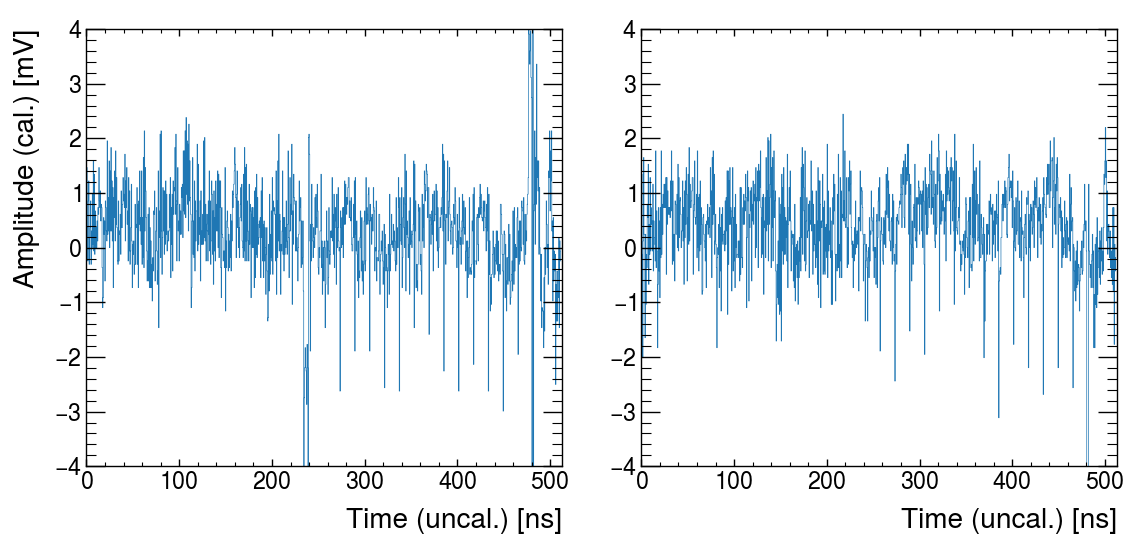
This one should be considered resolved.
| Stefan Ritt wrote: |
|
Dear Sean,
noise in transparent mode comes from some coupling to your system clock. But 3.5 mV RMS seems rather hight to me. You should get it to below 1 mV if the DRS4 input is clean (try to short it).
The noise in the readout is expected. It looks exactly as Plot3 from the data sheet. You have to calibrate it away with a fixed offset for each cell as described in this paper: https://arxiv.org/abs/1405.4975 (paragraph IV. A. Voltage Calibration).
Concerning t_samp: Fig 11 in the datasheet just tells you that the rising edge of the SRCLK should come later than t_s after the address change. t_s is the setup time and 5 ns. Fig 12 tells you that the ADC should sample the analog output of the DRS t_samp after the address change A0-A3 and t_samp after the rising edge of SRCLK.
The digitizing speed of the evaluation board is indeed 15 MHz instead of the maximum 30 MHz, because this was easier to program in the FPGA. The t_samp has to be there so that the analog output signal of the DRS4 settles to its final value after each SRCLK pulse. If you sample "too early", you sample with the ADC the output when it is sill moving. So you have to wait until the analog is settled, but just before the next DRS sample becomes visible at the output. You can fine tune this with a differential probe at the DRS4 analog output (on a single ended probe you might drown in noise) on one channel of yoru scope and the ADC sample clock on the other channel of your scope. Note that the ADC sample clock cannot be derived straight from your FPGA clock, but you need some clock manager to fine-adjust its phase in 1ns steps.
But again, looking at your output, everything seems fine. You see the 5mV rms noise indicated in the datasheet table 1, which translates to about 20 mV peak-to-peak. If you do the offset calibration, this should go down to below 1 mV.
Best,
Stefan
| Sean Quinn wrote: |
|
Dear DRS4 team,
I'm experiencing some issues that seem to be isolated to the ASIC, and would like to understand if we are doing something wrong. There are several items to address in the post.
First, I do not think the noise observed is being injected from elsewhere on the board. If I run the DRS in transparent mode, the baseline noise is low, on order 3.5 mV (60 ADU), perhaps radiated from a clock. See below image. The scale is 0 to 1000 ADU with LSB = 6 uV (same AD9245 as eval board.). The DRS is in RUNNING state, I have forced a trigger in the ILA. This is for a single channel, CH0, 1024 cells.
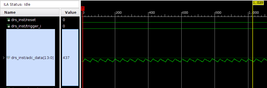
In the next image, I show the waveform obtained from a full readout. This corresponds to ADC_READOUT state, and the plot uses the same 1000 ADU scale. Noise seems around 350 ADU now, many factors worse than before.
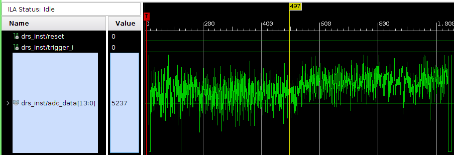
We've spent a lot of time trying to understand what's happening. One area that would be helpful to get some guidance on is the "t_samp" parameter. In Fig. 11 of the data sheet, should there be a t_samp label between t_s and t_clk? It just has arrows there with some width.
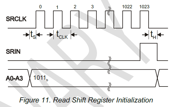
In our current firmware I believe R1 is simply one clock after R0 (for both ROI and full readout mode). Would this lead to the added noise observed in muxout?
This leads to the next question on what to actually use for t_samp. In the data sheet, page 4 "Timing Characteristics" it says to use t_samp = t0 + t_clk. Additionally, t0= 10 ns from that table. Fair enough.
But if I check this against the eval board timing, I see very different values. Here the clock is 15 MHz so t_clk=67 ns (I note another post about this topic https://elog.psi.ch/elogs/DRS4+Forum/713), so I expect t_samp = 77 ns. But in practice it looks like the R0 to R1 delay is ~465 ns? (cyan=RSRLOAD, yellow=SRCLK)
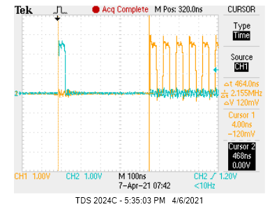
Given this, is t_samp a value that should be tuned by the user?
Best regards,
Sean
|
|
|
|
|
|
825
|
Fri Apr 9 21:38:59 2021 |
Stefan Ritt | Spikes/noise sensitive to clock settings? | elog:824
| Sean Quinn wrote: |
|
Dear DRS4 team,
I'm trying to troubleshoot some odd spike behavior. If I run the ADC and SR CLK at 16 MHz (behavior also seen at 33 MHz) we get very noisy data (post-calibration) with periodic spikes.
In the below plot
- CH0 & CH1 are muon pulses from a scintillator + SiPM detector
- CH8 is a 25 MHz sinewave (in phase with all generated board clocks)
- Transparent mode = ON
- ROI = OFF, "full readout mode", first sample = cell 0
- DRS REFCLK = 1 MHz (2 GS/s)
- ADC & SR CLK = 16 MHz, 0 deg. offset
After I modify some clock settings, things seem to improve dramatically, and the spike behavior changes
- ADC and SR CLK = 15 MHz, 0 deg. offset
- Transparent mode = ON
- ROI = ON (just for testing purposes)
- Add 1.064 ns skew to DRS REF CLK
- NOTE: Unfortunately due to a design mishap, the ADC and FPGA clock use a phase-locked output pair on our clock synthesis chip, so we cannot fine-tune the skew for it.
Observed differences
- Spike polarity seems inverted
- Spikes limited to smaller number of cells now?
- Spike amplitude reduced
- Overall baseline variance seems better
- New large positive spike artifact on CH0 that seems inverted on CH1
- CH8 seems unaffected by large spikes?
Artifacts seem related to clock configuration, but I am sort of in the dark on what might be happening from a first-principles point of view. Any tips?
Warm regards,
Sean
|
|
|
824
|
Fri Apr 9 20:55:28 2021 |
Stefan Ritt | Unexpected noise in muxout: t_samp related? | If you do the cell calibration correctly, your noise should be ~0.4 mV. You seem to be 2-3x larger. The periodic negative spikes come if you dont' sample at the right time. Adjust t_samp until they are gone.
Stefan
| Sean Quinn wrote: |
|
Hi Stefan,
Thanks much for the quick reply. Ok, yes, things do seem ok after the offset calibration. I am running into some other issues I could use your advice on but will make a separate thread. As a preview, you can see hints in this waveform (periodic negative spikes).
This one should be considered resolved.
| Stefan Ritt wrote: |
|
Dear Sean,
noise in transparent mode comes from some coupling to your system clock. But 3.5 mV RMS seems rather hight to me. You should get it to below 1 mV if the DRS4 input is clean (try to short it).
The noise in the readout is expected. It looks exactly as Plot3 from the data sheet. You have to calibrate it away with a fixed offset for each cell as described in this paper: https://arxiv.org/abs/1405.4975 (paragraph IV. A. Voltage Calibration).
Concerning t_samp: Fig 11 in the datasheet just tells you that the rising edge of the SRCLK should come later than t_s after the address change. t_s is the setup time and 5 ns. Fig 12 tells you that the ADC should sample the analog output of the DRS t_samp after the address change A0-A3 and t_samp after the rising edge of SRCLK.
The digitizing speed of the evaluation board is indeed 15 MHz instead of the maximum 30 MHz, because this was easier to program in the FPGA. The t_samp has to be there so that the analog output signal of the DRS4 settles to its final value after each SRCLK pulse. If you sample "too early", you sample with the ADC the output when it is sill moving. So you have to wait until the analog is settled, but just before the next DRS sample becomes visible at the output. You can fine tune this with a differential probe at the DRS4 analog output (on a single ended probe you might drown in noise) on one channel of yoru scope and the ADC sample clock on the other channel of your scope. Note that the ADC sample clock cannot be derived straight from your FPGA clock, but you need some clock manager to fine-adjust its phase in 1ns steps.
But again, looking at your output, everything seems fine. You see the 5mV rms noise indicated in the datasheet table 1, which translates to about 20 mV peak-to-peak. If you do the offset calibration, this should go down to below 1 mV.
Best,
Stefan
| Sean Quinn wrote: |
|
Dear DRS4 team,
I'm experiencing some issues that seem to be isolated to the ASIC, and would like to understand if we are doing something wrong. There are several items to address in the post.
First, I do not think the noise observed is being injected from elsewhere on the board. If I run the DRS in transparent mode, the baseline noise is low, on order 3.5 mV (60 ADU), perhaps radiated from a clock. See below image. The scale is 0 to 1000 ADU with LSB = 6 uV (same AD9245 as eval board.). The DRS is in RUNNING state, I have forced a trigger in the ILA. This is for a single channel, CH0, 1024 cells.
In the next image, I show the waveform obtained from a full readout. This corresponds to ADC_READOUT state, and the plot uses the same 1000 ADU scale. Noise seems around 350 ADU now, many factors worse than before.
We've spent a lot of time trying to understand what's happening. One area that would be helpful to get some guidance on is the "t_samp" parameter. In Fig. 11 of the data sheet, should there be a t_samp label between t_s and t_clk? It just has arrows there with some width.
In our current firmware I believe R1 is simply one clock after R0 (for both ROI and full readout mode). Would this lead to the added noise observed in muxout?
This leads to the next question on what to actually use for t_samp. In the data sheet, page 4 "Timing Characteristics" it says to use t_samp = t0 + t_clk. Additionally, t0= 10 ns from that table. Fair enough.
But if I check this against the eval board timing, I see very different values. Here the clock is 15 MHz so t_clk=67 ns (I note another post about this topic https://elog.psi.ch/elogs/DRS4+Forum/713), so I expect t_samp = 77 ns. But in practice it looks like the R0 to R1 delay is ~465 ns? (cyan=RSRLOAD, yellow=SRCLK)
Given this, is t_samp a value that should be tuned by the user?
Best regards,
Sean
|
|
|
|
|
823
|
Fri Apr 9 20:29:45 2021 |
Sean Quinn | Spikes/noise sensitive to clock settings? | Dear DRS4 team,
I'm trying to troubleshoot some odd spike behavior. If I run the ADC and SR CLK at 16 MHz (behavior also seen at 33 MHz) we get very noisy data (post-calibration) with periodic spikes.
In the below plot
- CH0 & CH1 are muon pulses from a scintillator + SiPM detector
- CH8 is a 25 MHz sinewave (in phase with all generated board clocks)
- Transparent mode = ON
- ROI = OFF, "full readout mode", first sample = cell 0
- DRS REFCLK = 1 MHz (2 GS/s)
- ADC & SR CLK = 16 MHz, 0 deg. offset
After I modify some clock settings, things seem to improve dramatically, and the spike behavior changes
- ADC and SR CLK = 15 MHz, 0 deg. offset
- Transparent mode = ON
- ROI = ON (just for testing purposes)
- Add 1.064 ns skew to DRS REF CLK
- NOTE: Unfortunately due to a design mishap, the ADC and FPGA clock use a phase-locked output pair on our clock synthesis chip, so we cannot fine-tune the skew for it.
Observed differences
- Spike polarity seems inverted
- Spikes limited to smaller number of cells now?
- Spike amplitude reduced
- Overall baseline variance seems better
- New large positive spike artifact on CH0 that seems inverted on CH1
- CH8 seems unaffected by large spikes?
Artifacts seem related to clock configuration, but I am sort of in the dark on what might be happening from a first-principles point of view. Any tips?
Warm regards,
Sean |
|
822
|
Fri Apr 9 20:22:13 2021 |
Sean Quinn | Unexpected noise in muxout: t_samp related? | Hi Stefan,
Thanks much for the quick reply. Ok, yes, things do seem ok after the offset calibration. I am running into some other issues I could use your advice on but will make a separate thread. As a preview, you can see hints in this waveform (periodic negative spikes).
This one should be considered resolved.
| Stefan Ritt wrote: |
|
Dear Sean,
noise in transparent mode comes from some coupling to your system clock. But 3.5 mV RMS seems rather hight to me. You should get it to below 1 mV if the DRS4 input is clean (try to short it).
The noise in the readout is expected. It looks exactly as Plot3 from the data sheet. You have to calibrate it away with a fixed offset for each cell as described in this paper: https://arxiv.org/abs/1405.4975 (paragraph IV. A. Voltage Calibration).
Concerning t_samp: Fig 11 in the datasheet just tells you that the rising edge of the SRCLK should come later than t_s after the address change. t_s is the setup time and 5 ns. Fig 12 tells you that the ADC should sample the analog output of the DRS t_samp after the address change A0-A3 and t_samp after the rising edge of SRCLK.
The digitizing speed of the evaluation board is indeed 15 MHz instead of the maximum 30 MHz, because this was easier to program in the FPGA. The t_samp has to be there so that the analog output signal of the DRS4 settles to its final value after each SRCLK pulse. If you sample "too early", you sample with the ADC the output when it is sill moving. So you have to wait until the analog is settled, but just before the next DRS sample becomes visible at the output. You can fine tune this with a differential probe at the DRS4 analog output (on a single ended probe you might drown in noise) on one channel of yoru scope and the ADC sample clock on the other channel of your scope. Note that the ADC sample clock cannot be derived straight from your FPGA clock, but you need some clock manager to fine-adjust its phase in 1ns steps.
But again, looking at your output, everything seems fine. You see the 5mV rms noise indicated in the datasheet table 1, which translates to about 20 mV peak-to-peak. If you do the offset calibration, this should go down to below 1 mV.
Best,
Stefan
| Sean Quinn wrote: |
|
Dear DRS4 team,
I'm experiencing some issues that seem to be isolated to the ASIC, and would like to understand if we are doing something wrong. There are several items to address in the post.
First, I do not think the noise observed is being injected from elsewhere on the board. If I run the DRS in transparent mode, the baseline noise is low, on order 3.5 mV (60 ADU), perhaps radiated from a clock. See below image. The scale is 0 to 1000 ADU with LSB = 6 uV (same AD9245 as eval board.). The DRS is in RUNNING state, I have forced a trigger in the ILA. This is for a single channel, CH0, 1024 cells.
In the next image, I show the waveform obtained from a full readout. This corresponds to ADC_READOUT state, and the plot uses the same 1000 ADU scale. Noise seems around 350 ADU now, many factors worse than before.
We've spent a lot of time trying to understand what's happening. One area that would be helpful to get some guidance on is the "t_samp" parameter. In Fig. 11 of the data sheet, should there be a t_samp label between t_s and t_clk? It just has arrows there with some width.
In our current firmware I believe R1 is simply one clock after R0 (for both ROI and full readout mode). Would this lead to the added noise observed in muxout?
This leads to the next question on what to actually use for t_samp. In the data sheet, page 4 "Timing Characteristics" it says to use t_samp = t0 + t_clk. Additionally, t0= 10 ns from that table. Fair enough.
But if I check this against the eval board timing, I see very different values. Here the clock is 15 MHz so t_clk=67 ns (I note another post about this topic https://elog.psi.ch/elogs/DRS4+Forum/713), so I expect t_samp = 77 ns. But in practice it looks like the R0 to R1 delay is ~465 ns? (cyan=RSRLOAD, yellow=SRCLK)
Given this, is t_samp a value that should be tuned by the user?
Best regards,
Sean
|
|
|
|
821
|
Wed Apr 7 08:26:12 2021 |
Stefan Ritt | Unexpected noise in muxout: t_samp related? | Dear Sean,
noise in transparent mode comes from some coupling to your system clock. But 3.5 mV RMS seems rather hight to me. You should get it to below 1 mV if the DRS4 input is clean (try to short it).
The noise in the readout is expected. It looks exactly as Plot3 from the data sheet. You have to calibrate it away with a fixed offset for each cell as described in this paper: https://arxiv.org/abs/1405.4975 (paragraph IV. A. Voltage Calibration).
Concerning t_samp: Fig 11 in the datasheet just tells you that the rising edge of the SRCLK should come later than t_s after the address change. t_s is the setup time and 5 ns. Fig 12 tells you that the ADC should sample the analog output of the DRS t_samp after the address change A0-A3 and t_samp after the rising edge of SRCLK.
The digitizing speed of the evaluation board is indeed 15 MHz instead of the maximum 30 MHz, because this was easier to program in the FPGA. The t_samp has to be there so that the analog output signal of the DRS4 settles to its final value after each SRCLK pulse. If you sample "too early", you sample with the ADC the output when it is sill moving. So you have to wait until the analog is settled, but just before the next DRS sample becomes visible at the output. You can fine tune this with a differential probe at the DRS4 analog output (on a single ended probe you might drown in noise) on one channel of yoru scope and the ADC sample clock on the other channel of your scope. Note that the ADC sample clock cannot be derived straight from your FPGA clock, but you need some clock manager to fine-adjust its phase in 1ns steps.
But again, looking at your output, everything seems fine. You see the 5mV rms noise indicated in the datasheet table 1, which translates to about 20 mV peak-to-peak. If you do the offset calibration, this should go down to below 1 mV.
Best,
Stefan
| Sean Quinn wrote: |
|
Dear DRS4 team,
I'm experiencing some issues that seem to be isolated to the ASIC, and would like to understand if we are doing something wrong. There are several items to address in the post.
First, I do not think the noise observed is being injected from elsewhere on the board. If I run the DRS in transparent mode, the baseline noise is low, on order 3.5 mV (60 ADU), perhaps radiated from a clock. See below image. The scale is 0 to 1000 ADU with LSB = 6 uV (same AD9245 as eval board.). The DRS is in RUNNING state, I have forced a trigger in the ILA. This is for a single channel, CH0, 1024 cells.
In the next image, I show the waveform obtained from a full readout. This corresponds to ADC_READOUT state, and the plot uses the same 1000 ADU scale. Noise seems around 350 ADU now, many factors worse than before.
We've spent a lot of time trying to understand what's happening. One area that would be helpful to get some guidance on is the "t_samp" parameter. In Fig. 11 of the data sheet, should there be a t_samp label between t_s and t_clk? It just has arrows there with some width.
In our current firmware I believe R1 is simply one clock after R0 (for both ROI and full readout mode). Would this lead to the added noise observed in muxout?
This leads to the next question on what to actually use for t_samp. In the data sheet, page 4 "Timing Characteristics" it says to use t_samp = t0 + t_clk. Additionally, t0= 10 ns from that table. Fair enough.
But if I check this against the eval board timing, I see very different values. Here the clock is 15 MHz so t_clk=67 ns (I note another post about this topic https://elog.psi.ch/elogs/DRS4+Forum/713), so I expect t_samp = 77 ns. But in practice it looks like the R0 to R1 delay is ~465 ns? (cyan=RSRLOAD, yellow=SRCLK)
Given this, is t_samp a value that should be tuned by the user?
Best regards,
Sean
|
|
|
820
|
Wed Apr 7 03:29:39 2021 |
Sean Quinn | Unexpected noise in muxout: t_samp related? | Dear DRS4 team,
I'm experiencing some issues that seem to be isolated to the ASIC, and would like to understand if we are doing something wrong. There are several items to address in the post.
First, I do not think the noise observed is being injected from elsewhere on the board. If I run the DRS in transparent mode, the baseline noise is low, on order 3.5 mV (60 ADU), perhaps radiated from a clock. See below image. The scale is 0 to 1000 ADU with LSB = 6 uV (same AD9245 as eval board.). The DRS is in RUNNING state, I have forced a trigger in the ILA. This is for a single channel, CH0, 1024 cells.
In the next image, I show the waveform obtained from a full readout. This corresponds to ADC_READOUT state, and the plot uses the same 1000 ADU scale. Noise seems around 350 ADU now, many factors worse than before.
We've spent a lot of time trying to understand what's happening. One area that would be helpful to get some guidance on is the "t_samp" parameter. In Fig. 11 of the data sheet, should there be a t_samp label between t_s and t_clk? It just has arrows there with some width.
In our current firmware I believe R1 is simply one clock after R0 (for both ROI and full readout mode). Would this lead to the added noise observed in muxout?
This leads to the next question on what to actually use for t_samp. In the data sheet, page 4 "Timing Characteristics" it says to use t_samp = t0 + t_clk. Additionally, t0= 10 ns from that table. Fair enough.
But if I check this against the eval board timing, I see very different values. Here the clock is 15 MHz so t_clk=67 ns (I note another post about this topic https://elog.psi.ch/elogs/DRS4+Forum/713), so I expect t_samp = 77 ns. But in practice it looks like the R0 to R1 delay is ~465 ns? (cyan=RSRLOAD, yellow=SRCLK)
Given this, is t_samp a value that should be tuned by the user?
Best regards,
Sean
|
|
819
|
Fri Mar 5 09:39:42 2021 |
Stefan Ritt | Trouble getting PLL to lock | That probably depends on the way your FPGA boots. If the SRCLK signal goes high after the SRIN - even a few ns - you might clock one or two zeros into the config register, thus disabling the PLL. Shame that I haven't thought of this before.
Stefan |
|
818
|
Thu Mar 4 21:36:14 2021 |
Tom Schneider | Trouble getting PLL to lock | I found the problem, and it had nothing to do with the CMOS clock input. As it turns out, even though I was using the default state of the config register, I still had to write to it after powerup. Once I did that, the PLL locked immediately.
-Tom
| Tom Schneider wrote: |
|
Thats not a simple modification to my PCB, but I'll give it a try. Thanks for your help
| Stefan Ritt wrote: |
|
Sounds to me like your REFCLK is not getting through or your PLL loop is open. Could be a bad solder connection. Try to measure signals not on the PCB trace, but directly on the DRS4 pins. Drive REFCLK with a proper LVDS signal. Maybe it's wrong what I wrote in the data sheet and the trick with VDD/2 is not really working.
Stefan
|
|
|
|
817
|
Fri Feb 26 22:52:13 2021 |
Tom Schneider | Trouble getting PLL to lock | Thats not a simple modification to my PCB, but I'll give it a try. Thanks for your help
| Stefan Ritt wrote: |
|
Sounds to me like your REFCLK is not getting through or your PLL loop is open. Could be a bad solder connection. Try to measure signals not on the PCB trace, but directly on the DRS4 pins. Drive REFCLK with a proper LVDS signal. Maybe it's wrong what I wrote in the data sheet and the trick with VDD/2 is not really working.
Stefan
|
|
|
816
|
Fri Feb 26 22:12:58 2021 |
Stefan Ritt | Trouble getting PLL to lock | Sounds to me like your REFCLK is not getting through or your PLL loop is open. Could be a bad solder connection. Try to measure signals not on the PCB trace, but directly on the DRS4 pins. Drive REFCLK with a proper LVDS signal. Maybe it's wrong what I wrote in the data sheet and the trick with VDD/2 is not really working.
Stefan |
|
815
|
Fri Feb 26 21:24:39 2021 |
Tom Schneider | Trouble getting PLL to lock | Probe capacitance makes that tricky - if I put my probe on DSPEED, I see that it starts at approx. 2.5V then gradually decreases until it hits 0V. DTAP decreases from 3MHz to 0 during this time.
I'll try to get something together to show you.
| Stefan Ritt wrote: |
|
Can you post a scope trace of your refclk together with DTAP, DSPEED and DENABLE?
| Tom Schneider wrote: |
|
Stefan,
Thanks for responding so quickly. Yes I have my clock source going to REFCLK+ (CLKIN is the signal name on my schematic). BIAS is 0.7V exactly, /RESET is high, A0-A3 are 0x0000, and the loop filter has a 4.7nF cap to GND with a 130ohm resistor + 1uF cap in parallel, just like the eval board.
Regarding the clock - I am not using an LVDS clock, but rather a 2.5V-level clock signal, with REFCLK- tied to 1.25V. Sheet 9 of the datasheet states: If no LVDS reference clock signal is available, a CMOS signal can be connected to REFCLK+ and the REFCLK input is connected to VDD/2 via a resistor divider.
Is that not a true statement?
-Tom
| Stefan Ritt wrote: |
|
I guess you mean "1 MHz clock at REFCLK+", and not CLKIN, there is no CLKIN, just a SRCLK, but that is someting else!
There could be many reasons why this is not working. It's hard for me to debug your board without actually having it in hands. So just some ideas:
- Supply a clean differential REFCLK, I never tried one end tied to VDD/2
- Is /RESET high?
- Is BIAS at roughly 0.7V?
- Is A0-A3 different from 1111, which puts the chip in standby
- Did you double check your loop filter?
The easiest usually is to start from a running evaluation board, then compare all pins 1:1 with your board.
Stefan
| Tom Schneider wrote: |
|
Hello,
I am working on a custom PCB design with the DRS4 chip, and I can't get the PLL to lock. I'm feeding CLKIN with a 1MHz CMOS clock (REFCLK- tied to VDD/2), and I'm using the same loop filter as the eval board. I see from the datasheet that the PLL is enabled by default, so I'm not writing anything to the config register on startup. I am just driving DENABLE high approx. 100ms after startup and looking for the PLL lock bit to go high. When I look at DTAP, I see a 3MHz signal. Can anyone tell me what I'm doing wrong?
-Tom
|
|
|
|
|
|
814
|
Fri Feb 26 20:32:25 2021 |
Stefan Ritt | Trouble getting PLL to lock | Can you post a scope trace of your refclk together with DTAP, DSPEED and DENABLE?
| Tom Schneider wrote: |
|
Stefan,
Thanks for responding so quickly. Yes I have my clock source going to REFCLK+ (CLKIN is the signal name on my schematic). BIAS is 0.7V exactly, /RESET is high, A0-A3 are 0x0000, and the loop filter has a 4.7nF cap to GND with a 130ohm resistor + 1uF cap in parallel, just like the eval board.
Regarding the clock - I am not using an LVDS clock, but rather a 2.5V-level clock signal, with REFCLK- tied to 1.25V. Sheet 9 of the datasheet states: If no LVDS reference clock signal is available, a CMOS signal can be connected to REFCLK+ and the REFCLK input is connected to VDD/2 via a resistor divider.
Is that not a true statement?
-Tom
| Stefan Ritt wrote: |
|
I guess you mean "1 MHz clock at REFCLK+", and not CLKIN, there is no CLKIN, just a SRCLK, but that is someting else!
There could be many reasons why this is not working. It's hard for me to debug your board without actually having it in hands. So just some ideas:
- Supply a clean differential REFCLK, I never tried one end tied to VDD/2
- Is /RESET high?
- Is BIAS at roughly 0.7V?
- Is A0-A3 different from 1111, which puts the chip in standby
- Did you double check your loop filter?
The easiest usually is to start from a running evaluation board, then compare all pins 1:1 with your board.
Stefan
| Tom Schneider wrote: |
|
Hello,
I am working on a custom PCB design with the DRS4 chip, and I can't get the PLL to lock. I'm feeding CLKIN with a 1MHz CMOS clock (REFCLK- tied to VDD/2), and I'm using the same loop filter as the eval board. I see from the datasheet that the PLL is enabled by default, so I'm not writing anything to the config register on startup. I am just driving DENABLE high approx. 100ms after startup and looking for the PLL lock bit to go high. When I look at DTAP, I see a 3MHz signal. Can anyone tell me what I'm doing wrong?
-Tom
|
|
|
|
|
813
|
Fri Feb 26 18:33:52 2021 |
Tom Schneider | Trouble getting PLL to lock | Stefan,
Thanks for responding so quickly. Yes I have my clock source going to REFCLK+ (CLKIN is the signal name on my schematic). BIAS is 0.7V exactly, /RESET is high, A0-A3 are 0x0000, and the loop filter has a 4.7nF cap to GND with a 130ohm resistor + 1uF cap in parallel, just like the eval board.
Regarding the clock - I am not using an LVDS clock, but rather a 2.5V-level clock signal, with REFCLK- tied to 1.25V. Sheet 9 of the datasheet states: If no LVDS reference clock signal is available, a CMOS signal can be connected to REFCLK+ and the REFCLK input is connected to VDD/2 via a resistor divider.
Is that not a true statement?
-Tom
| Stefan Ritt wrote: |
|
I guess you mean "1 MHz clock at REFCLK+", and not CLKIN, there is no CLKIN, just a SRCLK, but that is someting else!
There could be many reasons why this is not working. It's hard for me to debug your board without actually having it in hands. So just some ideas:
- Supply a clean differential REFCLK, I never tried one end tied to VDD/2
- Is /RESET high?
- Is BIAS at roughly 0.7V?
- Is A0-A3 different from 1111, which puts the chip in standby
- Did you double check your loop filter?
The easiest usually is to start from a running evaluation board, then compare all pins 1:1 with your board.
Stefan
| Tom Schneider wrote: |
|
Hello,
I am working on a custom PCB design with the DRS4 chip, and I can't get the PLL to lock. I'm feeding CLKIN with a 1MHz CMOS clock (REFCLK- tied to VDD/2), and I'm using the same loop filter as the eval board. I see from the datasheet that the PLL is enabled by default, so I'm not writing anything to the config register on startup. I am just driving DENABLE high approx. 100ms after startup and looking for the PLL lock bit to go high. When I look at DTAP, I see a 3MHz signal. Can anyone tell me what I'm doing wrong?
-Tom
|
|
|
|
812
|
Fri Feb 26 17:59:14 2021 |
Stefan Ritt | Trouble getting PLL to lock | I guess you mean "1 MHz clock at REFCLK+", and not CLKIN, there is no CLKIN, just a SRCLK, but that is someting else!
There could be many reasons why this is not working. It's hard for me to debug your board without actually having it in hands. So just some ideas:
- Supply a clean differential REFCLK, I never tried one end tied to VDD/2
- Is /RESET high?
- Is BIAS at roughly 0.7V?
- Is A0-A3 different from 1111, which puts the chip in standby
- Did you double check your loop filter?
The easiest usually is to start from a running evaluation board, then compare all pins 1:1 with your board.
Stefan
| Tom Schneider wrote: |
|
Hello,
I am working on a custom PCB design with the DRS4 chip, and I can't get the PLL to lock. I'm feeding CLKIN with a 1MHz CMOS clock (REFCLK- tied to VDD/2), and I'm using the same loop filter as the eval board. I see from the datasheet that the PLL is enabled by default, so I'm not writing anything to the config register on startup. I am just driving DENABLE high approx. 100ms after startup and looking for the PLL lock bit to go high. When I look at DTAP, I see a 3MHz signal. Can anyone tell me what I'm doing wrong?
-Tom
|
|
|
811
|
Fri Feb 26 17:05:26 2021 |
Tom Schneider | Trouble getting PLL to lock | Hello,
I am working on a custom PCB design with the DRS4 chip, and I can't get the PLL to lock. I'm feeding CLKIN with a 1MHz CMOS clock (REFCLK- tied to VDD/2), and I'm using the same loop filter as the eval board. I see from the datasheet that the PLL is enabled by default, so I'm not writing anything to the config register on startup. I am just driving DENABLE high approx. 100ms after startup and looking for the PLL lock bit to go high. When I look at DTAP, I see a 3MHz signal. Can anyone tell me what I'm doing wrong?
-Tom |
|
810
|
Fri Feb 26 08:52:50 2021 |
Stefan Ritt | DRS spike removal for multiple waveforms | Just look at the definition of the function below, all parameters are explained there. In meantime we have a firmware fix to avoid the spikes inside the chip, but I have not yet found time to update the evaluation board.
Stefan
void DRSBoard::RemoveSymmetricSpikes(short **wf, int nwf,
short diffThreshold, int spikeWidth,
short maxPeakToPeak, short spikeVoltage,
int nTimeRegionThreshold)
{
// Remove a specific kind of spike on DRS4.
// This spike has some features,
// - Common on all the channels on a chip
// - Constant heigh and width
// - Two spikes per channel
// - Symmetric to cell #0.
//
// This is not general purpose spike-removing function.
//
// wf : Waveform data. cell#0 must be at bin0,
// and number of bins must be kNumberOfBins.
// nwf : Number of channels which "wf" holds.
// diffThreshold : Amplitude threshold to find peak
// spikeWidth : Width of spike
// maxPeakToPeak : When peak-to-peak is larger than this, the channel
// is not used to find spikes.
// spikeVoltage : Amplitude of spikes. When it is 0, it is calculated in this function
// from voltage difference from neighboring bins.
// nTimeRegionThreshold : Requirement of number of time regions having spike at common position.
// Total number of time regions is 2*"nwf". |
|
809
|
Thu Feb 25 17:56:39 2021 |
Matthias Plum | DRS spike removal for multiple waveforms | Hi,
Is there a way that someone can help me and my student to enable RemoveSymmetricSpikes function in the drs_exam.cpp? We are not 100% sure how to call the function if you want to read out four waveforms.
Cheers,
Matthias |
|
808
|
Wed Jan 20 17:37:51 2021 |
Stefan Ritt | drs4 persistence | The chip itself can only sample a single waveform, that must be done in the attached software. The current DRSOscilloscope software coming with the evaluation board has not yet implemented that, but if you write your own software you can do so.
| Taegyu Lee wrote: |
|
Dear all,
I have a question about the function that drs4 can perform.
Is there any function in drs4 that is analogous to that of "persistence display" in oscilloscope?? (accumulating pulses)
Thank you
|
|
|
807
|
Wed Jan 20 12:14:49 2021 |
Taegyu Lee | drs4 persistence | Dear all,
I have a question about the function that drs4 can perform.
Is there any function in drs4 that is analogous to that of "persistence display" in oscilloscope?? (accumulating pulses)
Thank you |
|
806
|
Thu Dec 17 11:31:34 2020 |
Stefan Ritt | drs sources on github? | Not github, but bitbucket: https://bitbucket.org/ritt/drs4eb/src/master/
But development kind of stalled, so there will be updates only in case of severe bugs, which are kind of gone after 10 years now.
Best,
Stefan
> Are there plans to add the drs software to github? (asking because I have users @ethz.ch that want to use it on debian,
> thus I'm creating official debian packages of it, if license allows so, but talking to upstream (the developers) would be
> much easier on github (or irc) than on this "DRS4 Discussion Forum".
>
> Best, |
|
805
|
Thu Dec 17 09:29:43 2020 |
Alex Myczko | drs sources on github? | Are there plans to add the drs software to github? (asking because I have users @ethz.ch that want to use it on debian,
thus I'm creating official debian packages of it, if license allows so, but talking to upstream (the developers) would be
much easier on github (or irc) than on this "DRS4 Discussion Forum".
Best, |
|
804
|
Wed Oct 28 04:32:19 2020 |
Seiya Nozaki | Timing diagram of SROUT/SRIN signal to write/read a write shift register | Dear Stefan,
OK, it's good to hear! Thank you!
Best,
Seiya
| Stefan Ritt wrote: |
|
This is a static shift register, so you can make the clock as slow as you want. Actually I don't use a "clock", I just use a data pin I control via a state machine in the VHDL code. This way I have more control over the edges. I need several (internal) clock cycles to produce one SRCLK clock cycle, but that does not matter for the DRS.
Stefan
| Seiya Nozaki wrote: |
|
Dear Stefan,
Thank you for your reply.
SRIN is directly connected to SROUT via FPGA for now, but it is unstable for the timing between clock and SRIN depending on the firmware logic.
We want to make our system more robust, so we are thinking to use a clock with a lower frequency (let's say 16.6 MHz) or change the duty cycle of a clock to keep more time between the rising edge and falling edge of a clock. This change is just for reading/writing the write shift register, we will use a 33 MHz clock for the analog readout in any case.
If we change like above, are there any concerns from the DRS4 side?
Best,
Seiya
| Stefan Ritt wrote: |
|
Dear Seiya,
1) That's correct. SRIN is ampled at the falling edge. Pleae make sure to obey the hold-time as written in the datasheet. P.12, Fig. 11: SRIN must be stable before the falling edge of SRCLK and tH after the falling clock. tH is 5ns according to table 1.
2) The write shift register is a 8-bit shift register, with an input, output and clock. After the first clock pulse, the 7th bit is shown, after the second clock pulse the 6th bit and so on. You you need 8 clock pulses to read the whole register. At the same time you write to the register, so what ever is present at SRIN will replace the old 8 bits of that register.
3) No this is not possible. When you read the register, you write to it at the same time. One possibilty is to connect SROUT to SRIN during that (maybe via the FPGA). Then you have a circular register wich is the same after each 8 clock pulses.
For your reference, I posted a commercial D-Flip Flop (TI SNHCS72). The DRS4 write shift register is a simple array of 8 such registers, with no CLR or PRE, where SROUT is Q of the last Flip Flop.
Best,
Stefan
| Seiya Nozaki wrote: |
|
Dear Stefan,
I have questions about the timing diagram of SROUT/SRIN signal to write/read a write shift register.
1) Value of SRIN signal is saved at the falling edge of SRCLK, correct? (It is written in datasheet, page12, "Bits are latched into the shift register on the falling edge of SRCLK")
2) When are 8-bits of write shift register shown through SROUT? At ridging edges of SRCLK? and with additional delay(~10ns)? or falling edges?
3) In my understanding, when SRCLK is sent to DRS4, we can read and write the values in parallel, right? If so, is it possible just to read the registers without updating the registers?
[Background]
We have two modes to set the write shift register, the first one is to always reconnect to the first line and another one is to reconnect to the same line as when DWRITE goes to Low.
We can read/write the write shift register with the first mode (channel reset, page1). But we rarely face the problem of write shift register, unexpected values are written, with the second mode. With this mode, SROUT signal is sent back to DRS from FPGA as SRIN to write the same value on the write shift register. So there is a small delay(~10ns) due to the routing (DRS->FPGA->DRS, page2). It seems SRIN signal is not stable around the falling edges of SRCLK, thus it could cause that unexpected values are written in write shifter register.
To understand the situation clearly, I'd like to know the answer to the above questions.
Thank you.
Best regards,
Seiya
|
|
|
|
|
|
803
|
Tue Oct 27 15:24:38 2020 |
Stefan Ritt | Timing diagram of SROUT/SRIN signal to write/read a write shift register | This is a static shift register, so you can make the clock as slow as you want. Actually I don't use a "clock", I just use a data pin I control via a state machine in the VHDL code. This way I have more control over the edges. I need several (internal) clock cycles to produce one SRCLK clock cycle, but that does not matter for the DRS.
Stefan
| Seiya Nozaki wrote: |
|
Dear Stefan,
Thank you for your reply.
SRIN is directly connected to SROUT via FPGA for now, but it is unstable for the timing between clock and SRIN depending on the firmware logic.
We want to make our system more robust, so we are thinking to use a clock with a lower frequency (let's say 16.6 MHz) or change the duty cycle of a clock to keep more time between the rising edge and falling edge of a clock. This change is just for reading/writing the write shift register, we will use a 33 MHz clock for the analog readout in any case.
If we change like above, are there any concerns from the DRS4 side?
Best,
Seiya
| Stefan Ritt wrote: |
|
Dear Seiya,
1) That's correct. SRIN is ampled at the falling edge. Pleae make sure to obey the hold-time as written in the datasheet. P.12, Fig. 11: SRIN must be stable before the falling edge of SRCLK and tH after the falling clock. tH is 5ns according to table 1.
2) The write shift register is a 8-bit shift register, with an input, output and clock. After the first clock pulse, the 7th bit is shown, after the second clock pulse the 6th bit and so on. You you need 8 clock pulses to read the whole register. At the same time you write to the register, so what ever is present at SRIN will replace the old 8 bits of that register.
3) No this is not possible. When you read the register, you write to it at the same time. One possibilty is to connect SROUT to SRIN during that (maybe via the FPGA). Then you have a circular register wich is the same after each 8 clock pulses.
For your reference, I posted a commercial D-Flip Flop (TI SNHCS72). The DRS4 write shift register is a simple array of 8 such registers, with no CLR or PRE, where SROUT is Q of the last Flip Flop.
Best,
Stefan
| Seiya Nozaki wrote: |
|
Dear Stefan,
I have questions about the timing diagram of SROUT/SRIN signal to write/read a write shift register.
1) Value of SRIN signal is saved at the falling edge of SRCLK, correct? (It is written in datasheet, page12, "Bits are latched into the shift register on the falling edge of SRCLK")
2) When are 8-bits of write shift register shown through SROUT? At ridging edges of SRCLK? and with additional delay(~10ns)? or falling edges?
3) In my understanding, when SRCLK is sent to DRS4, we can read and write the values in parallel, right? If so, is it possible just to read the registers without updating the registers?
[Background]
We have two modes to set the write shift register, the first one is to always reconnect to the first line and another one is to reconnect to the same line as when DWRITE goes to Low.
We can read/write the write shift register with the first mode (channel reset, page1). But we rarely face the problem of write shift register, unexpected values are written, with the second mode. With this mode, SROUT signal is sent back to DRS from FPGA as SRIN to write the same value on the write shift register. So there is a small delay(~10ns) due to the routing (DRS->FPGA->DRS, page2). It seems SRIN signal is not stable around the falling edges of SRCLK, thus it could cause that unexpected values are written in write shifter register.
To understand the situation clearly, I'd like to know the answer to the above questions.
Thank you.
Best regards,
Seiya
|
|
|
|
|
802
|
Tue Oct 27 15:02:09 2020 |
Seiya Nozaki | Timing diagram of SROUT/SRIN signal to write/read a write shift register | Dear Stefan,
Thank you for your reply.
SRIN is directly connected to SROUT via FPGA for now, but it is unstable for the timing between clock and SRIN depending on the firmware logic.
We want to make our system more robust, so we are thinking to use a clock with a lower frequency (let's say 16.6 MHz) or change the duty cycle of a clock to keep more time between the rising edge and falling edge of a clock. This change is just for reading/writing the write shift register, we will use a 33 MHz clock for the analog readout in any case.
If we change like above, are there any concerns from the DRS4 side?
Best,
Seiya
| Stefan Ritt wrote: |
|
Dear Seiya,
1) That's correct. SRIN is ampled at the falling edge. Pleae make sure to obey the hold-time as written in the datasheet. P.12, Fig. 11: SRIN must be stable before the falling edge of SRCLK and tH after the falling clock. tH is 5ns according to table 1.
2) The write shift register is a 8-bit shift register, with an input, output and clock. After the first clock pulse, the 7th bit is shown, after the second clock pulse the 6th bit and so on. You you need 8 clock pulses to read the whole register. At the same time you write to the register, so what ever is present at SRIN will replace the old 8 bits of that register.
3) No this is not possible. When you read the register, you write to it at the same time. One possibilty is to connect SROUT to SRIN during that (maybe via the FPGA). Then you have a circular register wich is the same after each 8 clock pulses.
For your reference, I posted a commercial D-Flip Flop (TI SNHCS72). The DRS4 write shift register is a simple array of 8 such registers, with no CLR or PRE, where SROUT is Q of the last Flip Flop.
Best,
Stefan
| Seiya Nozaki wrote: |
|
Dear Stefan,
I have questions about the timing diagram of SROUT/SRIN signal to write/read a write shift register.
1) Value of SRIN signal is saved at the falling edge of SRCLK, correct? (It is written in datasheet, page12, "Bits are latched into the shift register on the falling edge of SRCLK")
2) When are 8-bits of write shift register shown through SROUT? At ridging edges of SRCLK? and with additional delay(~10ns)? or falling edges?
3) In my understanding, when SRCLK is sent to DRS4, we can read and write the values in parallel, right? If so, is it possible just to read the registers without updating the registers?
[Background]
We have two modes to set the write shift register, the first one is to always reconnect to the first line and another one is to reconnect to the same line as when DWRITE goes to Low.
We can read/write the write shift register with the first mode (channel reset, page1). But we rarely face the problem of write shift register, unexpected values are written, with the second mode. With this mode, SROUT signal is sent back to DRS from FPGA as SRIN to write the same value on the write shift register. So there is a small delay(~10ns) due to the routing (DRS->FPGA->DRS, page2). It seems SRIN signal is not stable around the falling edges of SRCLK, thus it could cause that unexpected values are written in write shifter register.
To understand the situation clearly, I'd like to know the answer to the above questions.
Thank you.
Best regards,
Seiya
|
|
|
|
801
|
Tue Oct 27 13:37:23 2020 |
Stefan Ritt | Timing diagram of SROUT/SRIN signal to write/read a write shift register | Dear Seiya,
1) That's correct. SRIN is ampled at the falling edge. Pleae make sure to obey the hold-time as written in the datasheet. P.12, Fig. 11: SRIN must be stable before the falling edge of SRCLK and tH after the falling clock. tH is 5ns according to table 1.
2) The write shift register is a 8-bit shift register, with an input, output and clock. After the first clock pulse, the 7th bit is shown, after the second clock pulse the 6th bit and so on. You you need 8 clock pulses to read the whole register. At the same time you write to the register, so what ever is present at SRIN will replace the old 8 bits of that register.
3) No this is not possible. When you read the register, you write to it at the same time. One possibilty is to connect SROUT to SRIN during that (maybe via the FPGA). Then you have a circular register wich is the same after each 8 clock pulses.
For your reference, I posted a commercial D-Flip Flop (TI SNHCS72). The DRS4 write shift register is a simple array of 8 such registers, with no CLR or PRE, where SROUT is Q of the last Flip Flop.
Best,
Stefan
| Seiya Nozaki wrote: |
|
Dear Stefan,
I have questions about the timing diagram of SROUT/SRIN signal to write/read a write shift register.
1) Value of SRIN signal is saved at the falling edge of SRCLK, correct? (It is written in datasheet, page12, "Bits are latched into the shift register on the falling edge of SRCLK")
2) When are 8-bits of write shift register shown through SROUT? At ridging edges of SRCLK? and with additional delay(~10ns)? or falling edges?
3) In my understanding, when SRCLK is sent to DRS4, we can read and write the values in parallel, right? If so, is it possible just to read the registers without updating the registers?
[Background]
We have two modes to set the write shift register, the first one is to always reconnect to the first line and another one is to reconnect to the same line as when DWRITE goes to Low.
We can read/write the write shift register with the first mode (channel reset, page1). But we rarely face the problem of write shift register, unexpected values are written, with the second mode. With this mode, SROUT signal is sent back to DRS from FPGA as SRIN to write the same value on the write shift register. So there is a small delay(~10ns) due to the routing (DRS->FPGA->DRS, page2). It seems SRIN signal is not stable around the falling edges of SRCLK, thus it could cause that unexpected values are written in write shifter register.
To understand the situation clearly, I'd like to know the answer to the above questions.
Thank you.
Best regards,
Seiya
|
|
| Attachment 1: Screenshot_2020-10-27_at_13.45.39_.png
|

|
|
800
|
Wed Oct 21 15:03:13 2020 |
Seiya Nozaki | Timing diagram of SROUT/SRIN signal to write/read a write shift register | Dear Stefan,
I have questions about the timing diagram of SROUT/SRIN signal to write/read a write shift register.
1) Value of SRIN signal is saved at the falling edge of SRCLK, correct? (It is written in datasheet, page12, "Bits are latched into the shift register on the falling edge of SRCLK")
2) When are 8-bits of write shift register shown through SROUT? At ridging edges of SRCLK? and with additional delay(~10ns)? or falling edges?
3) In my understanding, when SRCLK is sent to DRS4, we can read and write the values in parallel, right? If so, is it possible just to read the registers without updating the registers?
[Background]
We have two modes to set the write shift register, the first one is to always reconnect to the first line and another one is to reconnect to the same line as when DWRITE goes to Low.
We can read/write the write shift register with the first mode (channel reset, page1). But we rarely face the problem of write shift register, unexpected values are written, with the second mode. With this mode, SROUT signal is sent back to DRS from FPGA as SRIN to write the same value on the write shift register. So there is a small delay(~10ns) due to the routing (DRS->FPGA->DRS, page2). It seems SRIN signal is not stable around the falling edges of SRCLK, thus it could cause that unexpected values are written in write shifter register.
To understand the situation clearly, I'd like to know the answer to the above questions.
Thank you.
Best regards,
Seiya |
| Attachment 1: drs4_srin_srout_srclk.pdf
|


|
|
799
|
Wed Oct 7 11:17:52 2020 |
Elmer Grundeman | External triggering | I will try that, thanks!
| Stefan Ritt wrote: |
|
The trigger is there only to trigger the chip, but cannot be used as a precise time reference. If you want to measure precise timing, do this always BETWEEN two inputs, never between an input and the trigger. You might want to split and delay your trigger signal and feed one copy to another input of the evaluation board as your reference.
Stefan
| Elmer Grundeman wrote: |
|
Dear all,
I had a question about timing jitter and external triggering.
I trigger the board externally with a 3V pulse from a DG645 delay generator and as a test I use the gated charge function to integrate another pulse of the DG which goes into channel 1 (the timing jitter between different outputs of the DG is on the order of ~25 picoseconds).
The issue I’m encountering is that the signal on channel 1 is jittering in time with ~1 ns, which means the signal is jittering with respect to my integration gate (point A and B). If I look at the data it always starts at t = 0.000 but my signal (pulse) moves around in time.
If I don’t use the external trigger but trigger on channel 1 directly the signal does not move with respect to the gate, but I can see the start and end of the trace move in time. If I look at the data the first data point is not at t = 0.000 but some other time, which jitters with ~1 ns.
I did repeat the voltage and timing calibration, but that did not help either.
Do you know where this jitter comes from and if I can get rid of it?
Best regards,
Elmer
|
|
|
|
798
|
Wed Oct 7 10:56:03 2020 |
Stefan Ritt | External triggering | The trigger is there only to trigger the chip, but cannot be used as a precise time reference. If you want to measure precise timing, do this always BETWEEN two inputs, never between an input and the trigger. You might want to split and delay your trigger signal and feed one copy to another input of the evaluation board as your reference.
Stefan
| Elmer Grundeman wrote: |
|
Dear all,
I had a question about timing jitter and external triggering.
I trigger the board externally with a 3V pulse from a DG645 delay generator and as a test I use the gated charge function to integrate another pulse of the DG which goes into channel 1 (the timing jitter between different outputs of the DG is on the order of ~25 picoseconds).
The issue I’m encountering is that the signal on channel 1 is jittering in time with ~1 ns, which means the signal is jittering with respect to my integration gate (point A and B). If I look at the data it always starts at t = 0.000 but my signal (pulse) moves around in time.
If I don’t use the external trigger but trigger on channel 1 directly the signal does not move with respect to the gate, but I can see the start and end of the trace move in time. If I look at the data the first data point is not at t = 0.000 but some other time, which jitters with ~1 ns.
I did repeat the voltage and timing calibration, but that did not help either.
Do you know where this jitter comes from and if I can get rid of it?
Best regards,
Elmer
|
|
|
797
|
Tue Sep 22 17:45:26 2020 |
Elmer Grundeman | External triggering | Dear all,
I had a question about timing jitter and external triggering.
I trigger the board externally with a 3V pulse from a DG645 delay generator and as a test I use the gated charge function to integrate another pulse of the DG which goes into channel 1 (the timing jitter between different outputs of the DG is on the order of ~25 picoseconds).
The issue I’m encountering is that the signal on channel 1 is jittering in time with ~1 ns, which means the signal is jittering with respect to my integration gate (point A and B). If I look at the data it always starts at t = 0.000 but my signal (pulse) moves around in time.
If I don’t use the external trigger but trigger on channel 1 directly the signal does not move with respect to the gate, but I can see the start and end of the trace move in time. If I look at the data the first data point is not at t = 0.000 but some other time, which jitters with ~1 ns.
I did repeat the voltage and timing calibration, but that did not help either.
Do you know where this jitter comes from and if I can get rid of it?
Best regards,
Elmer |
|
796
|
Mon Aug 31 17:17:30 2020 |
Stefan Ritt | Channel Cascading | If you have a board with cascading option, it should show the "combined" option in the 2048-bin option enabled (not grayed), as in the attached screen shot. If the 2048-bin option is all greyed out, the system does not recognize the cascading option. If your board has a sticker "2048 bin" and you still see the 2048-bin option greyed out, it might mean that a resistor on that board has been forgotten. If you do not see the "2048 bin" sticker on your board, you might not have a board with cascading option. So please check that. If the resistor is really missing, you can send us the board and we will add it.
Stefan
| Hans Steiger wrote: |
|
Dear All,
I have a board with Channel Cascading Option. I have the problem, that it seems to be impossible to run all 4 Channels simultaneously for digitizing pulses. I can just run even or odd channels but not even and odd ones? If I run in combined option, My question: If a board comes with this combined option, is it still usable as a 4Ch Digitizer but with 1024bin traces?
All the best,
Hans
|
|
| Attachment 1: Screenshot_2020-08-31_at_16.52.28_.png
|

|
|
795
|
Mon Aug 31 16:44:12 2020 |
Hans Steiger | Channel Cascading | Dear All,
I have a board with Channel Cascading Option. I have the problem, that it seems to be impossible to run all 4 Channels simultaneously for digitizing pulses. I can just run even or odd channels but not even and odd ones? If I run in combined option, My question: If a board comes with this combined option, is it still usable as a 4Ch Digitizer but with 1024bin traces?
All the best,
Hans |
|
794
|
Mon Aug 31 10:52:42 2020 |
Stefan Ritt | Dynamic Range Evaluation Board and Software | You cannot go below -0.5V for the inputs, since the board does not have an internal negative power supply, which would be necessary for that. If you have -0.8V pulses, the easiest is to use a passive inverter at the input to convert it to a 0.8V pulse.
Stefan
| Hans Steiger wrote: |
|
Dear Evaluation Board Team,
currently I am facing the problem of digitizing pulses with an amplitude of -0.6V to -0.8V. As the dynamic range of the board is 1Vpp, this should be feasible. However, I do not know how to set in the software a correct range. I see only -0.5V/0.5V, and the two positive options. Normally I would use -0.5V/0.5V and give the thing an offset of 0.4V or so? Is this possible? Where can I set such a offset?
All the best,
Hans
|
|
|
793
|
Sat Aug 29 22:00:30 2020 |
Hans Steiger | Dynamic Range Evaluation Board and Software | Dear Evaluation Board Team,
currently I am facing the problem of digitizing pulses with an amplitude of -0.6V to -0.8V. As the dynamic range of the board is 1Vpp, this should be feasible. However, I do not know how to set in the software a correct range. I see only -0.5V/0.5V, and the two positive options. Normally I would use -0.5V/0.5V and give the thing an offset of 0.4V or so? Is this possible? Where can I set such a offset?
All the best,
Hans |
|
792
|
Tue Jul 28 22:40:44 2020 |
Razvan Stefan Gornea | no board found | I have a very similar problem, the command line doesn't work but the oscilloscope program does! Tried to fix it using Zadig driver update. Using Windows 7....
DRS command line tool, Revision 21435
Type 'help' for a list of available commands.
USB successfully scanned, but no boards found
No DRS Boards found
For completion, I just tested that the test program gives the same error message
C:\Program Files (x86)\DRS\bin>.\drs_exam.exe
USB successfully scanned, but no boards found
No DRS4 evaluation board found
| Stefan Ritt wrote: |
|
"dynamic" or "static" does not matter, as long as you don't use your program on another computer. I have no more idea about the "no board found" problem. It works ok on all computers I tried at our lab.
Stefan
| Lev Pavlov wrote: |
|
Hello. When compiling drs_exam, do you need to use a "static "version of usblib or a "dynamic" version?"The problem with "no board found" is not solved. Thanks for your help.
Lev
|
|
|
| Attachment 1: DRS4_scope.png
|

|
|
791
|
Tue May 26 12:44:16 2020 |
Stefan Ritt | Domino wave | Look at the attached picture. For simplicity, only 4 cells are open and tracking the input signal. Time is flowing from top to bottom. So initially, a train of 4 cells is open. When it's stopped, the train stops not immediately, but kind of "runs against a wall" at the stop cell. So each cell is open for four time ticks effectively, and you can use all 1024 cells.
| xggg wrote: |
|
Hi Stefan,
According to the datasheet DRS_rev09, the write signal is always 16 cells wide. So when the domino wave runs in infinite mode and be stopped by setting DENABLE low , there are always 16 cells capicitors tracking the input signal . It means that the effective sample cells is 1024-16=1008? That's confusing.
|
|
| Attachment 1: Screenshot_2020-05-26_at_12.43.40_.png
|

|
|
790
|
Tue May 26 11:10:27 2020 |
xggg | Domino wave | Hi Stefan,
According to the datasheet DRS_rev09, the write signal is always 16 cells wide. So when the domino wave runs in infinite mode and be stopped by setting DENABLE low , there are always 16 cells capicitors tracking the input signal . It means that the effective sample cells is 1024-16=1008? That's confusing. |
|
789
|
Mon May 25 03:36:12 2020 |
Keita Mizukoshi | DRS4 Evaluation board control tool 'drscl' with macro file | Thank you very much. That is what I wanted.
| Stefan Ritt wrote: |
|
There is an example program in the distribution under software/drscl/drs_exam.cpp which is a stand-alone program to do what you need. It uses the C library coming with the distribution. It configureres the board, defines a trigger, and then writes a few waveforms into a file. You can use it as a starting point for your development. If you need any other language, you have to develop bindings to the C library.
Stefan
| Keita Mizukoshi wrote: |
|
Dear experts,
I would like to use DRS4 evaluation board as DAQ system for small, table-top experiment.
I need waveforms capture as binary file on some trigger based on command line without GUI.
I found `drscl` tool in official software, but it require interactive command. I'd rather use static macro or so on to control DAQ as same behaviour in each time.
I guess, experts are thinking users should develop DAQ code by themselves for their experiment specifically, but my request is very common so someone has already developed these tool.
Best regards,
Keita
|
|
|
|
788
|
Fri May 22 13:24:51 2020 |
Stefan Ritt | Type check at DOFrame.h in official software | The software is a bit outdated, I will soon make a new release.
In meantime, you can replace that like with
bool GetRefclk(int board) { return m_refClk[board]; }
Best,
Stefan
| Keita Mizukoshi wrote: |
|
Hi,
I've failured to compile official software. The cause is the following line.
DOFrame.h L.111 bool GetRefclk() { return m_refClk > 0; }
m_refClk is pointer to bool. I guess these line is for null-check of the pointer.
Can I replace the following line as
bool GetRefclk() { return m_refClk != nullptr; }
?
The latest compilers may not accept C-style check.
My compiler version is
Apple clang version 11.0.3 (clang-1103.0.32.59)
Target: x86_64-apple-darwin19.4.0
Thread model: posix
InstalledDir: /Applications/Xcode.app/Contents/Developer/Toolchains/XcodeDefault.xctoolchain/usr/bin
Best regards,
Keita
|
|
|
786
|
Fri May 22 12:53:33 2020 |
Stefan Ritt | DRS4 Evaluation board control tool 'drscl' with macro file | There is an example program in the distribution under software/drscl/drs_exam.cpp which is a stand-alone program to do what you need. It uses the C library coming with the distribution. It configureres the board, defines a trigger, and then writes a few waveforms into a file. You can use it as a starting point for your development. If you need any other language, you have to develop bindings to the C library.
Stefan
| Keita Mizukoshi wrote: |
|
Dear experts,
I would like to use DRS4 evaluation board as DAQ system for small, table-top experiment.
I need waveforms capture as binary file on some trigger based on command line without GUI.
I found `drscl` tool in official software, but it require interactive command. I'd rather use static macro or so on to control DAQ as same behaviour in each time.
I guess, experts are thinking users should develop DAQ code by themselves for their experiment specifically, but my request is very common so someone has already developed these tool.
Best regards,
Keita
|
|
|
785
|
Thu May 21 07:38:05 2020 |
Keita Mizukoshi | Type check at DOFrame.h in official software | Hi,
I've failured to compile official software. The cause is the following line.
DOFrame.h L.111 bool GetRefclk() { return m_refClk > 0; }
m_refClk is pointer to bool. I guess these line is for null-check of the pointer.
Can I replace the following line as
bool GetRefclk() { return m_refClk != nullptr; }
?
The latest compilers may not accept C-style check.
My compiler version is
Apple clang version 11.0.3 (clang-1103.0.32.59)
Target: x86_64-apple-darwin19.4.0
Thread model: posix
InstalledDir: /Applications/Xcode.app/Contents/Developer/Toolchains/XcodeDefault.xctoolchain/usr/bin
Best regards,
Keita |
|
784
|
Thu May 21 07:18:48 2020 |
Keita Mizukoshi | DRS4 Evaluation board control tool 'drscl' with macro file | Dear experts,
I would like to use DRS4 evaluation board as DAQ system for small, table-top experiment.
I need waveforms capture as binary file on some trigger based on command line without GUI.
I found `drscl` tool in official software, but it require interactive command. I'd rather use static macro or so on to control DAQ as same behaviour in each time.
I guess, experts are thinking users should develop DAQ code by themselves for their experiment specifically, but my request is very common so someone has already developed these tool.
Best regards,
Keita |
|
783
|
Mon Mar 23 15:03:28 2020 |
Ajay Krishnamurthy | USB trigger issue | Hello,
I had forgotten to disable the turn off the power to the USB drive on Windows and DRS4 stopped triggering. Now, we are all on quarantine and I am unable to reset the board to normal function. Are there any commands to reset the board remotely. I tried all of the default Windows based solutions such as disable USB port etc., but I am unable to do this. Only thing that has worked in the past is manually replugging the USB but I do not have the option to do that currently. Please help.
Thanks,
Ajay |
|
782
|
Fri Oct 25 16:39:07 2019 |
Stefan Ritt | Computing corrected time from binary data...what is t_0,0? | t0,0 refers to the time of cell #0 of channel #0. So basically you keep channel 0 fixed, calculate the difference of each channel's cell #0 in respect to channel 0, and align all channels except channel 0 so that their cell #0 has the same value. There is an inconsistency between the channel numbering. The formula uses 0...3 and the manual says "channel 1" but it means actually the first channel, which uses index "0".
Stefan
| John Jendzurski wrote: |
|
In the equations for computing the corrected time for channels other than channel 1, does anyone know what the term t0,0 refers to? This is the last term in the last equation on page 24 of DRS4 Evaluation Board User’s Manual, Board Revision 5 as of January 2014, Last revised: April 27, 2016.
Screenshot from User's Manual is attached below.
Thank you!
|
|
|
781
|
Wed Oct 23 17:56:26 2019 |
John Jendzurski | Computing corrected time from binary data...what is t_0,0? | In the equations for computing the corrected time for channels other than channel 1, does anyone know what the term t0,0 refers to? This is the last term in the last equation on page 24 of DRS4 Evaluation Board User’s Manual, Board Revision 5 as of January 2014, Last revised: April 27, 2016.
Screenshot from User's Manual is attached below.
Thank you! |
| Attachment 1: Screenshot.png
|

|
|
780
|
Tue Oct 15 08:14:17 2019 |
Danyang | how to acquire the stop position with channel cascading | Thanks a lot. The problem is solved when A3-A0 is set 1101 and srclk keeps low.
Best Regards,
Danyang
| Stefan Ritt wrote: |
|
If you configure the Write Shift Register with 01010101b, then all you have to do after a trigger is to set A3-A0 to 1101. The WSROUT pin shows you then either ther state 01010101b or 10101010b, you the pin should be 1 or 0, and that's all you need. The Write Shift Register is NOT routed to the SROUT pin, you only see it at the WSROUT pin.
Stefan
| Danyang wrote: |
|
Yes, firstly I configured the chip with 4x2048 bins by setting the Write Shift Register to 01010101b, A3-A0 keeps 1101----> secondly I enabled the domino wave, wait some time for stable, A3-A0 keeps 1111 ---->thirdly stops the domino wave when the trigger comes, A3-A0 keeps 1101 (or 1010, 0000)----> forthly send the clock pulse to the srclk pin, A3-A0 keeps 1101, srout pin keeps low----> fifthly enable rsrload, A3-A0 (0000-1000), srout pin reacts nomally. I think the cascading is worked when I checked the waveform on the oscilloscope. Is there any step I missed?
Best Regards,
Danyang
| Stefan Ritt wrote: |
|
Note that you have to read out the Write Shift Register only if you do channel cascading, e.g. configuring the chip with 4x2048 bins by setting the Write Shift Register to 01010101b. Then the Write Shift Register tells you in which 1024-bin segment the Domino Wave has been stopped. If you use the normal 8x1024 bin mode, you don't have to read out the Write Shift Register since it continas only 1's.
Stefan
| Danyang wrote: |
|
I tried the logic in my designed board. The results are shown in the picture: Srout keeps low when A3-A0 is set to 1101 and srclk is set as you mentioned. And the drs4 chip does not output sine wave in such configuration.
Srout signal only reacts after the rsrload signal is pulled high and A3-A0 is not 1101.
The number of srclk is not enough? Is there any recommended time to configure the command?
Best Regards,
Danyang
| Stefan Ritt wrote: |
|
You first set A3-A0, on the next clock cycle you issue pulses on srclk, and about 10ns after each clock pulse the output shows up at srout. Best is to verity this with an oscilloscope.
The radout of the shift register is independent of the readout mode, so you can use with with MUXOUT as well.
Stefan
| Danyang wrote: |
|
Hi Steffan,
In DSR4 DATASHEET Rev.0.9 Page13, there is a paragraph "If the DRS4 is configured for channel cascading or daisy chaining, it is necessary to know which the current channel is where the sampling has been stopped. This can be
determined by addressing the Write Shift Register withA3-A0 = 1101b and by applying clock pulses to the SRCLK input ...".
My question is the timing details about srclk, srout, A3-A0 in the above control and its timing relation with stop shift register (Figure 15). And can this configuration be used in the full readout mode with output MUXOUT?
Best Regards,
Danyang (sun2222@mail.ustc.edu.cn)
|
|
|
|
|
|
|
|
779
|
Mon Oct 14 15:27:09 2019 |
Stefan Ritt | how to acquire the stop position with channel cascading | If you configure the Write Shift Register with 01010101b, then all you have to do after a trigger is to set A3-A0 to 1101. The WSROUT pin shows you then either ther state 01010101b or 10101010b, you the pin should be 1 or 0, and that's all you need. The Write Shift Register is NOT routed to the SROUT pin, you only see it at the WSROUT pin.
Stefan
| Danyang wrote: |
|
Yes, firstly I configured the chip with 4x2048 bins by setting the Write Shift Register to 01010101b, A3-A0 keeps 1101----> secondly I enabled the domino wave, wait some time for stable, A3-A0 keeps 1111 ---->thirdly stops the domino wave when the trigger comes, A3-A0 keeps 1101 (or 1010, 0000)----> forthly send the clock pulse to the srclk pin, A3-A0 keeps 1101, srout pin keeps low----> fifthly enable rsrload, A3-A0 (0000-1000), srout pin reacts nomally. I think the cascading is worked when I checked the waveform on the oscilloscope. Is there any step I missed?
Best Regards,
Danyang
| Stefan Ritt wrote: |
|
Note that you have to read out the Write Shift Register only if you do channel cascading, e.g. configuring the chip with 4x2048 bins by setting the Write Shift Register to 01010101b. Then the Write Shift Register tells you in which 1024-bin segment the Domino Wave has been stopped. If you use the normal 8x1024 bin mode, you don't have to read out the Write Shift Register since it continas only 1's.
Stefan
| Danyang wrote: |
|
I tried the logic in my designed board. The results are shown in the picture: Srout keeps low when A3-A0 is set to 1101 and srclk is set as you mentioned. And the drs4 chip does not output sine wave in such configuration.
Srout signal only reacts after the rsrload signal is pulled high and A3-A0 is not 1101.
The number of srclk is not enough? Is there any recommended time to configure the command?
Best Regards,
Danyang
| Stefan Ritt wrote: |
|
You first set A3-A0, on the next clock cycle you issue pulses on srclk, and about 10ns after each clock pulse the output shows up at srout. Best is to verity this with an oscilloscope.
The radout of the shift register is independent of the readout mode, so you can use with with MUXOUT as well.
Stefan
| Danyang wrote: |
|
Hi Steffan,
In DSR4 DATASHEET Rev.0.9 Page13, there is a paragraph "If the DRS4 is configured for channel cascading or daisy chaining, it is necessary to know which the current channel is where the sampling has been stopped. This can be
determined by addressing the Write Shift Register withA3-A0 = 1101b and by applying clock pulses to the SRCLK input ...".
My question is the timing details about srclk, srout, A3-A0 in the above control and its timing relation with stop shift register (Figure 15). And can this configuration be used in the full readout mode with output MUXOUT?
Best Regards,
Danyang (sun2222@mail.ustc.edu.cn)
|
|
|
|
|
|
|
778
|
Mon Oct 14 13:44:26 2019 |
Danyang | how to acquire the stop position with channel cascading | Yes, firstly I configured the chip with 4x2048 bins by setting the Write Shift Register to 01010101b, A3-A0 keeps 1101----> secondly I enabled the domino wave, wait some time for stable, A3-A0 keeps 1111 ---->thirdly stops the domino wave when the trigger comes, A3-A0 keeps 1101 (or 1010, 0000)----> forthly send the clock pulse to the srclk pin, A3-A0 keeps 1101, srout pin keeps low----> fifthly enable rsrload, A3-A0 (0000-1000), srout pin reacts nomally. I think the cascading is worked when I checked the waveform on the oscilloscope. Is there any step I missed?
Best Regards,
Danyang
| Stefan Ritt wrote: |
|
Note that you have to read out the Write Shift Register only if you do channel cascading, e.g. configuring the chip with 4x2048 bins by setting the Write Shift Register to 01010101b. Then the Write Shift Register tells you in which 1024-bin segment the Domino Wave has been stopped. If you use the normal 8x1024 bin mode, you don't have to read out the Write Shift Register since it continas only 1's.
Stefan
| Danyang wrote: |
|
I tried the logic in my designed board. The results are shown in the picture: Srout keeps low when A3-A0 is set to 1101 and srclk is set as you mentioned. And the drs4 chip does not output sine wave in such configuration.
Srout signal only reacts after the rsrload signal is pulled high and A3-A0 is not 1101.
The number of srclk is not enough? Is there any recommended time to configure the command?
Best Regards,
Danyang
| Stefan Ritt wrote: |
|
You first set A3-A0, on the next clock cycle you issue pulses on srclk, and about 10ns after each clock pulse the output shows up at srout. Best is to verity this with an oscilloscope.
The radout of the shift register is independent of the readout mode, so you can use with with MUXOUT as well.
Stefan
| Danyang wrote: |
|
Hi Steffan,
In DSR4 DATASHEET Rev.0.9 Page13, there is a paragraph "If the DRS4 is configured for channel cascading or daisy chaining, it is necessary to know which the current channel is where the sampling has been stopped. This can be
determined by addressing the Write Shift Register withA3-A0 = 1101b and by applying clock pulses to the SRCLK input ...".
My question is the timing details about srclk, srout, A3-A0 in the above control and its timing relation with stop shift register (Figure 15). And can this configuration be used in the full readout mode with output MUXOUT?
Best Regards,
Danyang (sun2222@mail.ustc.edu.cn)
|
|
|
|
|
|
777
|
Mon Oct 14 12:56:13 2019 |
Stefan Ritt | how to acquire the stop position with channel cascading | Note that you have to read out the Write Shift Register only if you do channel cascading, e.g. configuring the chip with 4x2048 bins by setting the Write Shift Register to 01010101b. Then the Write Shift Register tells you in which 1024-bin segment the Domino Wave has been stopped. If you use the normal 8x1024 bin mode, you don't have to read out the Write Shift Register since it continas only 1's.
Stefan
| Danyang wrote: |
|
I tried the logic in my designed board. The results are shown in the picture: Srout keeps low when A3-A0 is set to 1101 and srclk is set as you mentioned. And the drs4 chip does not output sine wave in such configuration.
Srout signal only reacts after the rsrload signal is pulled high and A3-A0 is not 1101.
The number of srclk is not enough? Is there any recommended time to configure the command?
Best Regards,
Danyang
| Stefan Ritt wrote: |
|
You first set A3-A0, on the next clock cycle you issue pulses on srclk, and about 10ns after each clock pulse the output shows up at srout. Best is to verity this with an oscilloscope.
The radout of the shift register is independent of the readout mode, so you can use with with MUXOUT as well.
Stefan
| Danyang wrote: |
|
Hi Steffan,
In DSR4 DATASHEET Rev.0.9 Page13, there is a paragraph "If the DRS4 is configured for channel cascading or daisy chaining, it is necessary to know which the current channel is where the sampling has been stopped. This can be
determined by addressing the Write Shift Register withA3-A0 = 1101b and by applying clock pulses to the SRCLK input ...".
My question is the timing details about srclk, srout, A3-A0 in the above control and its timing relation with stop shift register (Figure 15). And can this configuration be used in the full readout mode with output MUXOUT?
Best Regards,
Danyang (sun2222@mail.ustc.edu.cn)
|
|
|
|
|
776
|
Mon Oct 14 11:45:06 2019 |
Danyang | how to acquire the stop position with channel cascading | I tried the logic in my designed board. The results are shown in the picture: Srout keeps low when A3-A0 is set to 1101 and srclk is set as you mentioned. And the drs4 chip does not output sine wave in such configuration.
Srout signal only reacts after the rsrload signal is pulled high and A3-A0 is not 1101.
The number of srclk is not enough? Is there any recommended time to configure the command?
Best Regards,
Danyang
| Stefan Ritt wrote: |
|
You first set A3-A0, on the next clock cycle you issue pulses on srclk, and about 10ns after each clock pulse the output shows up at srout. Best is to verity this with an oscilloscope.
The radout of the shift register is independent of the readout mode, so you can use with with MUXOUT as well.
Stefan
| Danyang wrote: |
|
Hi Steffan,
In DSR4 DATASHEET Rev.0.9 Page13, there is a paragraph "If the DRS4 is configured for channel cascading or daisy chaining, it is necessary to know which the current channel is where the sampling has been stopped. This can be
determined by addressing the Write Shift Register withA3-A0 = 1101b and by applying clock pulses to the SRCLK input ...".
My question is the timing details about srclk, srout, A3-A0 in the above control and its timing relation with stop shift register (Figure 15). And can this configuration be used in the full readout mode with output MUXOUT?
Best Regards,
Danyang (sun2222@mail.ustc.edu.cn)
|
|
|
| Attachment 1: Capture.PNG
|

|
|
775
|
Mon Oct 14 10:14:46 2019 |
Stefan Ritt | how to acquire the stop position with channel cascading | You first set A3-A0, on the next clock cycle you issue pulses on srclk, and about 10ns after each clock pulse the output shows up at srout. Best is to verity this with an oscilloscope.
The radout of the shift register is independent of the readout mode, so you can use with with MUXOUT as well.
Stefan
| Danyang wrote: |
|
Hi Steffan,
In DSR4 DATASHEET Rev.0.9 Page13, there is a paragraph "If the DRS4 is configured for channel cascading or daisy chaining, it is necessary to know which the current channel is where the sampling has been stopped. This can be
determined by addressing the Write Shift Register withA3-A0 = 1101b and by applying clock pulses to the SRCLK input ...".
My question is the timing details about srclk, srout, A3-A0 in the above control and its timing relation with stop shift register (Figure 15). And can this configuration be used in the full readout mode with output MUXOUT?
Best Regards,
Danyang (sun2222@mail.ustc.edu.cn)
|
|
|
774
|
Mon Oct 14 09:32:33 2019 |
Danyang | how to acquire the stop position with channel cascading | Hi Steffan,
In DSR4 DATASHEET Rev.0.9 Page13, there is a paragraph "If the DRS4 is configured for channel cascading or daisy chaining, it is necessary to know which the current channel is where the sampling has been stopped. This can be
determined by addressing the Write Shift Register withA3-A0 = 1101b and by applying clock pulses to the SRCLK input ...".
My question is the timing details about srclk, srout, A3-A0 in the above control and its timing relation with stop shift register (Figure 15). And can this configuration be used in the full readout mode with output MUXOUT?
Best Regards,
Danyang (sun2222@mail.ustc.edu.cn) |
| Attachment 1: Capture.PNG
|

|
|
773
|
Fri Sep 13 15:27:41 2019 |
Arseny Rybnikov | Scaler / How to modify the firmware to change the scaler integration time | Hello,
We want to use the inner DRS4 counter(scaler) within more than the 100ms integration time. We guess that we need to modify the original firmware around this point:
-- Reference clock used for frequency counter
proc_1hzclk: process(I_RESET, I_CLK33)
begin
if (I_RESET = '1') then
drs_1hz_counter(31 downto 0) <= (others => '0');
drs_1hz_clock <= '0';
scaler_reset <= (others => '1');
scaler_ff_reset <= (others => '1');
elsif rising_edge(I_CLK33) then
drs_1hz_counter <= drs_1hz_counter - 1; -- count down
scaler_reset <= (others => '0');
scaler_ff_reset <= (others => '0');
-- toggle refclk if timer expires
if (drs_1hz_counter(drs_1hz_counter'high) = '1') then
drs_1hz_clock <= not drs_1hz_clock;
drs_1hz_counter(31 downto 0) <= X"0016E35F"; -- 1499999, I_CLK33 is actually a 30 MHz clock
scaler_ff_reset <= (others => '1'); -- reset scaler_ff once every 100ms cycle
loop_scaler_reset : for i in 0 to 5 loop
if (scaler_ff(i) = '0') then -- no activity since last cycle?
scaler_reset(i) <= '1'; -- force clear scaler register
end if;
end loop;
if (scaler_ff(0) = '0') then -- no activity since last cycle?
scaler_reset(0) <= '1'; -- force clear scaler register
end if;
end if;
end if;
end process;
Could you please tell us how to modify the firmware to increse the time up to 5 seconds for instance?
Thanks in advance, Arseny |
|
772
|
Tue Aug 27 09:14:03 2019 |
Stefan Ritt | DRS4 | Is a 5 GSPS oscilloscope suitable for use with Silicon surface barier detectors?
| chinmay basu wrote: |
|
Is DRS4 suitable for use with Silicon surface barrier detectors?
|
|
|
771
|
Tue Aug 27 08:33:22 2019 |
chinmay basu | DRS4 | Is DRS4 suitable for use with Silicon surface barrier detectors? |
|
770
|
Tue Aug 20 16:05:21 2019 |
Bill Ashmanskas | should one deassert DENABLE while writing the write-shift register? | Aha -- many thanks. I think what tripped up my test logic is that the "done" state in drs4_eval5_app.vhd that executes post-readout sets DWRITE back to 1 (drs_write_set). If one then writes to FPGA register 5 while the FSM is in the "idle" state, the conf_strobe and wsr_strobe states occur with DWRITE and DENABLE both asserted. This is if one sets the "dactive" bit in the FPGA app code, which is probably not the usual use case. Maybe using the real DRS.cpp avoids this situation. (I was simulating your FPGA code to test my understanding of what our FPGA code should do.)
Anyway, our own use case is fine: as you suggest, we leave DENABLE asserted, but we deassert DWRITE while reading out or while changing DRS4 register values.
Thanks again,
Bill
| Stefan Ritt wrote: |
|
Hi Bill,
you keep DENABLE active all the time to keep the Domino Wave running, but you deassert DWRITE if you change any register via SRCLK. There is no shadow register, just a simple shift register, but with DWRITE being low, the domino circuitry does not touch it.
Best,
Stefan
| Bill Ashmanskas wrote: |
|
Hi Stefan,
We have for some time now been using custom firmware on a custom board to read waveforms out of DRS4 chips. Now we are working on cascaded readout mode, 4 channels @ 2048 samples, WSREG=0x55, in order to allow for longer trigger latency.
Doing a testbench simulation of the FPGA code raised a question for me: Do I need to deassert DENABLE while I shift a new 8-bit value into the write-shift register? What happens if, during the few-hundred nanoseconds it takes to shift 8 bits into the register, the domino wave crosses cell 768, thereby shifting the write-shift register left by one bit? Is this shifting suppressed when A=0b1101? Or does the update of the actual write-shift register occur only once, after the 8th SRCLK cycle? (Maybe one is really shifting bits into a shadow register that is copied all at once into the actual register?)
I notice in simulating your drs4_eval5_app.vhd that if one sets bit 27 ("drs_ctl_dactive") of register 0 (do not deassert DENABLE on trigger), then starts the domino wave (set bit 0 of register 0), then issues a software trigger, then later writes to register 5 (config register, wsreg, etc.), DENABLE is not in fact deasserted during the time when A=0b1100 (conf_setup, conf_strobe) or when A=0b1101 (wsr_setup, wsr_strobe).
But my simulation testbench includes a simplified Verilog model of my interpretation of the DRS4 data sheet, and my simulated DRS4 happened to cause the write-shift register to shift (256 samples before DTAP toggled) during your "wsr_strobe" FSM state, thus corrupting the value that was being shifted into the WSREG via SRIN and SRCLK.
So I'm curious: to be safe, should one deassert DENABLE before updating the write-shift register, or is it safe to update it even while the domino wave is active and looping? It seems easy enough to be safe, since we should only need to write to the WSREG once during the setup phase and then let it loop forever.
Many thanks,
Bill
|
|
|
|
769
|
Tue Aug 20 10:44:45 2019 |
Stefan Ritt | should one deassert DENABLE while writing the write-shift register? | Hi Bill,
you keep DENABLE active all the time to keep the Domino Wave running, but you deassert DWRITE if you change any register via SRCLK. There is no shadow register, just a simple shift register, but with DWRITE being low, the domino circuitry does not touch it.
Best,
Stefan
| Bill Ashmanskas wrote: |
|
Hi Stefan,
We have for some time now been using custom firmware on a custom board to read waveforms out of DRS4 chips. Now we are working on cascaded readout mode, 4 channels @ 2048 samples, WSREG=0x55, in order to allow for longer trigger latency.
Doing a testbench simulation of the FPGA code raised a question for me: Do I need to deassert DENABLE while I shift a new 8-bit value into the write-shift register? What happens if, during the few-hundred nanoseconds it takes to shift 8 bits into the register, the domino wave crosses cell 768, thereby shifting the write-shift register left by one bit? Is this shifting suppressed when A=0b1101? Or does the update of the actual write-shift register occur only once, after the 8th SRCLK cycle? (Maybe one is really shifting bits into a shadow register that is copied all at once into the actual register?)
I notice in simulating your drs4_eval5_app.vhd that if one sets bit 27 ("drs_ctl_dactive") of register 0 (do not deassert DENABLE on trigger), then starts the domino wave (set bit 0 of register 0), then issues a software trigger, then later writes to register 5 (config register, wsreg, etc.), DENABLE is not in fact deasserted during the time when A=0b1100 (conf_setup, conf_strobe) or when A=0b1101 (wsr_setup, wsr_strobe).
But my simulation testbench includes a simplified Verilog model of my interpretation of the DRS4 data sheet, and my simulated DRS4 happened to cause the write-shift register to shift (256 samples before DTAP toggled) during your "wsr_strobe" FSM state, thus corrupting the value that was being shifted into the WSREG via SRIN and SRCLK.
So I'm curious: to be safe, should one deassert DENABLE before updating the write-shift register, or is it safe to update it even while the domino wave is active and looping? It seems easy enough to be safe, since we should only need to write to the WSREG once during the setup phase and then let it loop forever.
Many thanks,
Bill
|
|
|
768
|
Mon Aug 19 23:01:22 2019 |
Bill Ashmanskas | should one deassert DENABLE while writing the write-shift register? | Hi Stefan,
We have for some time now been using custom firmware on a custom board to read waveforms out of DRS4 chips. Now we are working on cascaded readout mode, 4 channels @ 2048 samples, WSREG=0x55, in order to allow for longer trigger latency.
Doing a testbench simulation of the FPGA code raised a question for me: Do I need to deassert DENABLE while I shift a new 8-bit value into the write-shift register? What happens if, during the few-hundred nanoseconds it takes to shift 8 bits into the register, the domino wave crosses cell 768, thereby shifting the write-shift register left by one bit? Is this shifting suppressed when A=0b1101? Or does the update of the actual write-shift register occur only once, after the 8th SRCLK cycle? (Maybe one is really shifting bits into a shadow register that is copied all at once into the actual register?)
I notice in simulating your drs4_eval5_app.vhd that if one sets bit 27 ("drs_ctl_dactive") of register 0 (do not deassert DENABLE on trigger), then starts the domino wave (set bit 0 of register 0), then issues a software trigger, then later writes to register 5 (config register, wsreg, etc.), DENABLE is not in fact deasserted during the time when A=0b1100 (conf_setup, conf_strobe) or when A=0b1101 (wsr_setup, wsr_strobe).
But my simulation testbench includes a simplified Verilog model of my interpretation of the DRS4 data sheet, and my simulated DRS4 happened to cause the write-shift register to shift (256 samples before DTAP toggled) during your "wsr_strobe" FSM state, thus corrupting the value that was being shifted into the WSREG via SRIN and SRCLK.
So I'm curious: to be safe, should one deassert DENABLE before updating the write-shift register, or is it safe to update it even while the domino wave is active and looping? It seems easy enough to be safe, since we should only need to write to the WSREG once during the setup phase and then let it loop forever.
Many thanks,
Bill
|
|
767
|
Sat Jul 20 12:28:14 2019 |
Stefan Ritt | Trace Impedance | The DRS4 input is high impedance. So if you like you can terminate it with 100 Ohm differentially and route it with 100 Ohm. But if you keep the lines short, the reflection is negligible. That’s what we made on the evaluation board.
| Ismael Garcia wrote: |
|
When you're refering to laying a 50 Ohm trace, you're referring to the SMA input and not the interface between the output of the Op-AMP(THS4508) buffer
and the inputs of the DRS4(IN0-IN8). Is there a recommended diffential impedance for IN0-IN8?
Ismael
| Stefan Ritt wrote: |
|
The requiremnet is the same as for any high speed analog board, there is othing special with the DRS4. If you want to terminate your line with 50 Ohms and you want a matched impedance layout, you route all lines with 50 Ohms impedance. Truth is however that nothing is perfect. The SMA connector is not exactly 50 Ohm, the PCB gets a 10-20% variation depending on the manufacturer. So even if you try hard, you will never have a 50 Ohm matched impedance. On the evaluation board we made some compromises as you have seen, but for us the board works satisfactory even with this compromises, and you can test it yourself with real hardware (namely the evaluation board). If you can do a better job, try it. But usually these compromises have only little influence on the signal quality.
Stefan
| Ismael Garcia wrote: |
|
Hi Steffan,
I'm an engineer at UCLA developing a board with the DRS4 chip. Our team has a question on what might be the required trace impedence for the analog inputs. Can that information be provided?
Best Regards,
Ismael Garcia
|
|
|
|
|
766
|
Fri Jul 19 01:37:09 2019 |
Ismael Garcia | Trace Impedance | When you're refering to laying a 50 Ohm trace, you're referring to the SMA input and not the interface between the output of the Op-AMP(THS4508) buffer
and the inputs of the DRS4(IN0-IN8). Is there a recommended diffential impedance for IN0-IN8?
Ismael
| Stefan Ritt wrote: |
|
The requiremnet is the same as for any high speed analog board, there is othing special with the DRS4. If you want to terminate your line with 50 Ohms and you want a matched impedance layout, you route all lines with 50 Ohms impedance. Truth is however that nothing is perfect. The SMA connector is not exactly 50 Ohm, the PCB gets a 10-20% variation depending on the manufacturer. So even if you try hard, you will never have a 50 Ohm matched impedance. On the evaluation board we made some compromises as you have seen, but for us the board works satisfactory even with this compromises, and you can test it yourself with real hardware (namely the evaluation board). If you can do a better job, try it. But usually these compromises have only little influence on the signal quality.
Stefan
| Ismael Garcia wrote: |
|
Hi Steffan,
I'm an engineer at UCLA developing a board with the DRS4 chip. Our team has a question on what might be the required trace impedence for the analog inputs. Can that information be provided?
Best Regards,
Ismael Garcia
|
|
|
|
765
|
Thu Jul 18 11:37:56 2019 |
Stefan Ritt | Trace Impedance | The requiremnet is the same as for any high speed analog board, there is othing special with the DRS4. If you want to terminate your line with 50 Ohms and you want a matched impedance layout, you route all lines with 50 Ohms impedance. Truth is however that nothing is perfect. The SMA connector is not exactly 50 Ohm, the PCB gets a 10-20% variation depending on the manufacturer. So even if you try hard, you will never have a 50 Ohm matched impedance. On the evaluation board we made some compromises as you have seen, but for us the board works satisfactory even with this compromises, and you can test it yourself with real hardware (namely the evaluation board). If you can do a better job, try it. But usually these compromises have only little influence on the signal quality.
Stefan
| Ismael Garcia wrote: |
|
Hi Steffan,
I'm an engineer at UCLA developing a board with the DRS4 chip. Our team has a question on what might be the required trace impedence for the analog inputs. Can that information be provided?
Best Regards,
Ismael Garcia
|
|
|
764
|
Thu Jul 18 01:03:44 2019 |
Ismael Garcia | Trace Impedance | |
Hi Steffan,
I'm an engineer at UCLA developing a board with the DRS4 chip. Our team has a question on what might be the required trace impedence for the analog inputs. Can that information be provided?
Best Regards,
Ismael Garcia
|
| Attachment 1: DRS4_Analog_IN.PNG
|

|
|
763
|
Mon Jul 15 19:34:25 2019 |
Brendan Posehn | Evaluation Board Test Functionality | Hello Stefan,
Thanks for the quick reply. The issue was a faulty SMA connector, should have checked this first. Signal looks good now.
Thanks for your time,
Brendan
| Stefan Ritt wrote: |
|
Have you set the trigger correctly to the channel with your signal, polarity and level? Do you undersand the difference between normal and auto trigger? Why don't you post a screendump. Are you ABSOLUTELY SURE that you have a signal on your cable? Have you tried with another oscilloscope? Are you sure that your SMA connector is good?
Stefan
| Brendan Posehn wrote: |
|
Hello,
I have recently obtained a DRS4 Evaluation Board (V5), but I am unable to register signals when using the DRS Oscilloscope application. There seems to be some difference in noise when I have an input connected to a signal or not, but I am unable to view a simple, 0.2V amplitude square wave or other small signals. The only way I have been able to view a waveform is when connecting the reference clock to all channels. When running 'info' in the DRS Command Line Interface I am shown correct information. I was wondering if there is any way for me to test the functionality of the board (specifially ability to read signals on Ch 1-4) to ensure that it is indeed working as expected?
Thanks,
Brendan
|
|
|
|
762
|
Mon Jul 15 17:26:50 2019 |
Stefan Ritt | Evaluation Board Test Functionality | Have you set the trigger correctly to the channel with your signal, polarity and level? Do you undersand the difference between normal and auto trigger? Why don't you post a screendump. Are you ABSOLUTELY SURE that you have a signal on your cable? Have you tried with another oscilloscope? Are you sure that your SMA connector is good?
Stefan
| Brendan Posehn wrote: |
|
Hello,
I have recently obtained a DRS4 Evaluation Board (V5), but I am unable to register signals when using the DRS Oscilloscope application. There seems to be some difference in noise when I have an input connected to a signal or not, but I am unable to view a simple, 0.2V amplitude square wave or other small signals. The only way I have been able to view a waveform is when connecting the reference clock to all channels. When running 'info' in the DRS Command Line Interface I am shown correct information. I was wondering if there is any way for me to test the functionality of the board (specifially ability to read signals on Ch 1-4) to ensure that it is indeed working as expected?
Thanks,
Brendan
|
|
|
761
|
Sat Jul 13 01:00:15 2019 |
Brendan Posehn | Evaluation Board Test Functionality | Hello,
I have recently obtained a DRS4 Evaluation Board (V5), but I am unable to register signals when using the DRS Oscilloscope application. There seems to be some difference in noise when I have an input connected to a signal or not, but I am unable to view a simple, 0.2V amplitude square wave or other small signals. The only way I have been able to view a waveform is when connecting the reference clock to all channels. When running 'info' in the DRS Command Line Interface I am shown correct information. I was wondering if there is any way for me to test the functionality of the board (specifially ability to read signals on Ch 1-4) to ensure that it is indeed working as expected?
Thanks,
Brendan |
|
760
|
Mon Jul 8 14:29:12 2019 |
Stefan Ritt | drs_exam is always reading out a sin wave | Actually in the original drs_exam.cpp the sine wave oscillator is turned off with this command
/* use following line to turn on the internal 100 MHz clock connected to all channels */
//b->EnableTcal(1);
If you remove the "//" then the generator gets enabled. Probably you did this by accident. With this line commented out, you see the proper input like this:
Event #0 ----------------------
t1[ns] u1[mV] t2[ns] u2[mV]
0.000 1.9 0.000 -2.4
0.195 0.5 0.195 0.3
0.391 0.1 0.391 -1.4
0.586 -0.7 0.586 -0.4
0.781 -1.1 0.781 -2.4
0.977 -0.6 0.977 0.0
1.172 -1.5 1.172 -2.8
1.367 -0.4 1.367 -0.6
1.562 -1.2 1.562 -3.8
1.758 -1.5 1.758 -1.7
1.953 -1.0 1.953 -3.3
2.148 -0.7 2.148 -1.8
2.344 -1.6 2.344 -4.2
2.539 0.5 2.539 -1.5
2.734 0.2 2.734 -3.6
...
167.969 -3.4 167.969 -5.2
168.164 -3.7 168.164 -3.6
168.359 0.0 168.359 -2.0
168.555 1.9 168.555 -0.2
168.750 2.8 168.750 -2.8
168.945 5.4 168.945 -1.4
169.141 18.0 169.141 1.2
169.336 26.6 169.336 2.7
169.531 46.2 169.531 0.4
169.727 56.2 169.727 1.6
169.922 93.3 169.922 0.1
170.117 115.6 170.117 0.0
170.312 174.4 170.312 -1.5
170.508 206.9 170.508 -0.8
170.703 282.2 170.703 -2.4
170.898 328.4 170.898 -1.2
171.094 419.6 171.094 -3.2
171.289 465.8 171.289 -2.5
171.484 500.0 171.484 -2.0
171.680 500.0 171.680 -0.6
171.875 500.0 171.875 -4.0
172.070 500.0 172.070 -1.1
172.266 500.0 172.266 -3.7
172.461 500.0 172.461 -2.1
172.656 500.0 172.656 -5.0
172.852 500.0 172.852 -3.3
173.047 500.0 173.047 -4.8
173.242 500.0 173.242 -4.1
173.438 500.0 173.438 -5.1
173.633 500.0 173.633 -3.3
173.828 500.0 173.828 -6.4
174.023 500.0 174.023 -3.9
174.219 500.0 174.219 -5.5
174.414 500.0 174.414 -3.2
174.609 500.0 174.609 -3.6
174.805 500.0 174.805 -2.6
175.000 500.0 175.000 -5.2
175.195 500.0 175.195 -2.7
175.391 434.3 175.391 -3.9
175.586 391.7 175.586 -2.4
175.781 312.2 175.781 -4.1
175.977 275.7 175.977 -1.8
176.172 202.4 176.172 -3.8
176.367 167.6 176.367 -1.4
176.562 117.4 176.562 -2.9
176.758 96.1 176.758 -2.3
176.953 62.8 176.953 -3.3
177.148 49.1 177.148 -1.8
177.344 35.9 177.344 -4.3
177.539 33.4 177.539 -2.6
177.734 30.4 177.734 -4.2
...
| Si Xie wrote: |
|
I see. Where is the code that we can use to turn off the generator? I thought the example is taking data with CH1 as the trigger.
For our board, which is BoardType == 9, it is running these lines:
b->EnableTrigger(1, 0); // enable hardware trigger
b->SetTriggerSource(1<<0); // set CH1 as source
Is that not using the hardware trigger with CH1 as the source?
| Stefan Ritt wrote: |
|
Sure, that’s correct. The example program turns on the internal sine wave generator in case people don’t have a real signal. That’s why it’s called „example“. Find the code which turns on the generator and change it. You will also have to change the trigger settings depending on your actual signal.
Stefan
| Si Xie wrote: |
|
We are using the drs_exam.cpp to read out waveforms, but it seems to be outputting only sin waves on all channels - as if it was reading out the simulated waveform from the oscilloscope program if we run it without the board plugged in. Does anyone know what is causing this?
We are taking data with a pulser plugged into channel 1, which produces a single pulse with width of 8ns, and nothing plugged into channel 2.
Our board is as follows:
Found DRS4 evaluation board, serial #2567, firmware revision 21305
Board type: 9
The output is something like the following:
Event #0 ----------------------
t1[ns] u1[mV] t2[ns] u2[mV]
0.000 -452.7 0.026 -469.3
0.289 -460.8 0.293 -469.8
0.413 -477.3 0.400 -481.5
0.642 -485.3 0.650 -482.4
0.806 -486.9 0.821 -477.8
1.086 -476.8 1.085 -457.2
1.183 -467.3 1.162 -446.4
1.450 -435.6 1.459 -405.1
1.619 -410.1 1.630 -373.3
1.843 -366.2 1.851 -323.9
1.945 -342.9 1.948 -298.9
2.221 -275.7 2.210 -229.3
2.359 -237.6 2.357 -187.6
2.602 -165.6 2.609 -111.2
2.687 -141.1 2.697 -84.3
2.976 -50.5 2.987 5.5
3.164 8.4 3.144 53.3
3.377 73.9 3.384 124.2
3.503 111.4 3.506 158.0
3.753 182.0 3.769 226.9
3.924 227.5 3.929 265.8
|
|
|
|
|
759
|
Wed Jun 26 15:17:51 2019 |
Si Xie | Running drs_example.cpp | Hi Rodrigo, I'm wondering how you solved your original triggering problem. We are also having trouble with collecting data continously using the example. Thanks.
| Rodrigo Trindade de Menezes wrote: |
|
We found a way to solve the previous problem, but right now when we try to set the input range only -0.5 to 0.5 is working. When we set the function "SetInputRange(0.5)" for 0 to 1V the output is all zeros and with "SetInputRange(0.45)" we just get all the outputs -49.9mV. What does that means? How to fix?
| odrigo Trindade de Menezes wrote: |
|
Hello,
We have been using the DRS4 evaluation board (S/N 2636) that works with the scope application. However we are trying to run the DRS4 evaluation board remotely by modifying the drs_exam.cpp to acquire and store data continuously.
We compiled the DRS_example.cpp without the wxWidgets but when we try to run the program, it appears to trigger on nonsense. The program appears to not be sensitive to the trigger threshold (although for very large trigger threshold it gets stuck in a waiting mode). Is there a way to ensure that the "normal" trigger mode is set? We are worried that the auto mode is running. Otherwise, not sure why the program is triggering on nonsense. By the way, it does not work with the wxWidgets compiled either so we are worried that there is an additional flag that needs to be set. The routine does not appear to conduct a calibration -- is this not necessary?
Another issue that we are having is with the data set stored on the .txt file looks incorrect. The time channel stops at 200 (but we think it should go up to 1024). In addition, the voltage channel appears to hover around small values near zero (as if triggering on noise). The output file appears this way even when we change the threshold to much higher values. It suggests that the trigger threshold is not actually being set? There are events where the output voltage appears to oscillate through huge negative and positive values too. So not sure what's going on.
Thanks!
Rodrigo
|
|
|
|
758
|
Wed Jun 26 15:10:09 2019 |
Si Xie | drs_exam is always reading out a sin wave | I see. Where is the code that we can use to turn off the generator? I thought the example is taking data with CH1 as the trigger.
For our board, which is BoardType == 9, it is running these lines:
b->EnableTrigger(1, 0); // enable hardware trigger
b->SetTriggerSource(1<<0); // set CH1 as source
Is that not using the hardware trigger with CH1 as the source?
| Stefan Ritt wrote: |
|
Sure, that’s correct. The example program turns on the internal sine wave generator in case people don’t have a real signal. That’s why it’s called „example“. Find the code which turns on the generator and change it. You will also have to change the trigger settings depending on your actual signal.
Stefan
| Si Xie wrote: |
|
We are using the drs_exam.cpp to read out waveforms, but it seems to be outputting only sin waves on all channels - as if it was reading out the simulated waveform from the oscilloscope program if we run it without the board plugged in. Does anyone know what is causing this?
We are taking data with a pulser plugged into channel 1, which produces a single pulse with width of 8ns, and nothing plugged into channel 2.
Our board is as follows:
Found DRS4 evaluation board, serial #2567, firmware revision 21305
Board type: 9
The output is something like the following:
Event #0 ----------------------
t1[ns] u1[mV] t2[ns] u2[mV]
0.000 -452.7 0.026 -469.3
0.289 -460.8 0.293 -469.8
0.413 -477.3 0.400 -481.5
0.642 -485.3 0.650 -482.4
0.806 -486.9 0.821 -477.8
1.086 -476.8 1.085 -457.2
1.183 -467.3 1.162 -446.4
1.450 -435.6 1.459 -405.1
1.619 -410.1 1.630 -373.3
1.843 -366.2 1.851 -323.9
1.945 -342.9 1.948 -298.9
2.221 -275.7 2.210 -229.3
2.359 -237.6 2.357 -187.6
2.602 -165.6 2.609 -111.2
2.687 -141.1 2.697 -84.3
2.976 -50.5 2.987 5.5
3.164 8.4 3.144 53.3
3.377 73.9 3.384 124.2
3.503 111.4 3.506 158.0
3.753 182.0 3.769 226.9
3.924 227.5 3.929 265.8
|
|
|
|
757
|
Wed Jun 26 13:08:42 2019 |
Stefan Ritt | drs_exam is always reading out a sin wave | Sure, that’s correct. The example program turns on the internal sine wave generator in case people don’t have a real signal. That’s why it’s called „example“. Find the code which turns on the generator and change it. You will also have to change the trigger settings depending on your actual signal.
Stefan
| Si Xie wrote: |
|
We are using the drs_exam.cpp to read out waveforms, but it seems to be outputting only sin waves on all channels - as if it was reading out the simulated waveform from the oscilloscope program if we run it without the board plugged in. Does anyone know what is causing this?
We are taking data with a pulser plugged into channel 1, which produces a single pulse with width of 8ns, and nothing plugged into channel 2.
Our board is as follows:
Found DRS4 evaluation board, serial #2567, firmware revision 21305
Board type: 9
The output is something like the following:
Event #0 ----------------------
t1[ns] u1[mV] t2[ns] u2[mV]
0.000 -452.7 0.026 -469.3
0.289 -460.8 0.293 -469.8
0.413 -477.3 0.400 -481.5
0.642 -485.3 0.650 -482.4
0.806 -486.9 0.821 -477.8
1.086 -476.8 1.085 -457.2
1.183 -467.3 1.162 -446.4
1.450 -435.6 1.459 -405.1
1.619 -410.1 1.630 -373.3
1.843 -366.2 1.851 -323.9
1.945 -342.9 1.948 -298.9
2.221 -275.7 2.210 -229.3
2.359 -237.6 2.357 -187.6
2.602 -165.6 2.609 -111.2
2.687 -141.1 2.697 -84.3
2.976 -50.5 2.987 5.5
3.164 8.4 3.144 53.3
3.377 73.9 3.384 124.2
3.503 111.4 3.506 158.0
3.753 182.0 3.769 226.9
3.924 227.5 3.929 265.8
|
|
|
756
|
Tue Jun 25 23:04:29 2019 |
Si Xie | drs_exam is always reading out a sin wave | We are using the drs_exam.cpp to read out waveforms, but it seems to be outputting only sin waves on all channels - as if it was reading out the simulated waveform from the oscilloscope program if we run it without the board plugged in. Does anyone know what is causing this?
We are taking data with a pulser plugged into channel 1, which produces a single pulse with width of 8ns, and nothing plugged into channel 2.
Our board is as follows:
Found DRS4 evaluation board, serial #2567, firmware revision 21305
Board type: 9
The output is something like the following:
Event #0 ----------------------
t1[ns] u1[mV] t2[ns] u2[mV]
0.000 -452.7 0.026 -469.3
0.289 -460.8 0.293 -469.8
0.413 -477.3 0.400 -481.5
0.642 -485.3 0.650 -482.4
0.806 -486.9 0.821 -477.8
1.086 -476.8 1.085 -457.2
1.183 -467.3 1.162 -446.4
1.450 -435.6 1.459 -405.1
1.619 -410.1 1.630 -373.3
1.843 -366.2 1.851 -323.9
1.945 -342.9 1.948 -298.9
2.221 -275.7 2.210 -229.3
2.359 -237.6 2.357 -187.6
2.602 -165.6 2.609 -111.2
2.687 -141.1 2.697 -84.3
2.976 -50.5 2.987 5.5
3.164 8.4 3.144 53.3
3.377 73.9 3.384 124.2
3.503 111.4 3.506 158.0
3.753 182.0 3.769 226.9
3.924 227.5 3.929 265.8
|
|
755
|
Mon Jun 24 23:07:35 2019 |
Andrew Peck | Evaluation firmware wait_vdd state | Dear Stefan,
Thanks so much for clarifying this. We made wait_vdd a parameter controlled by software and will try to experiment with it to find some compromise between deadtime and the offset added by the droop in VDD.
Best regards,
Andrew
| Stefan Ritt wrote: |
|
Dear Andrew,
the posting you mention is still accurate. Any power supply will drop when you start the Domino wave, no matter how big your capacitor is. Unfortunately the output signal of the DRS4 scales with VDD. So if your VDD drops by 40 mV and you get a trigger and you immediately start the readout, the output baseline will also be shifted by about 40 mV. If you are sensitive to dead time, you can remove the wait_vdd state completely, but then you have to deal with varying baseline shifts. If you have narrow signals sitting on a broad baseline, you can correct for this by measuring the baseline outside your signal, then subtracting it before integrating your pulse. If you have lots of pile-up in your signals, it might sometimes be hard to evaluate the baseline on an event-by-event basis.
Stefan
| Andrew Peck wrote: |
|
Dear Stefan,
I am working with others at UCLA on a custom made board built around the DRS4. We are in the process of writing firmware so I am adapting the readout state machine from the evaluation board firmware.
I see in the state machine of the eval board firmware that after a trigger is received, the FPGA goes into the start readout state and then into "wait_vdd", where the FPGA waits "~120 us for vdd to stabilize" before reading out the ADC.
Our application is sensitive to deadtime and this wait_vdd state adds very significantly. I am trying to find anything explaining the necessity of wait_vdd in the documentation / elog and have only found so far your old forum posting, https://elog.psi.ch/elogs/DRS4+Forum/12
Does this forum posting explain wait_vdd or is there a another purpose that I have missed?
If this post is relevant to wait_vdd, does the advice of large capacitance and an LDO with fast transient response still apply or are there any new recommendations?
Thank you,
Andrew Peck
|
|
|
|
754
|
Fri Jun 21 12:54:47 2019 |
Stefan Ritt | Evaluation firmware wait_vdd state | Dear Andrew,
the posting you mention is still accurate. Any power supply will drop when you start the Domino wave, no matter how big your capacitor is. Unfortunately the output signal of the DRS4 scales with VDD. So if your VDD drops by 40 mV and you get a trigger and you immediately start the readout, the output baseline will also be shifted by about 40 mV. If you are sensitive to dead time, you can remove the wait_vdd state completely, but then you have to deal with varying baseline shifts. If you have narrow signals sitting on a broad baseline, you can correct for this by measuring the baseline outside your signal, then subtracting it before integrating your pulse. If you have lots of pile-up in your signals, it might sometimes be hard to evaluate the baseline on an event-by-event basis.
Stefan
| Andrew Peck wrote: |
|
Dear Stefan,
I am working with others at UCLA on a custom made board built around the DRS4. We are in the process of writing firmware so I am adapting the readout state machine from the evaluation board firmware.
I see in the state machine of the eval board firmware that after a trigger is received, the FPGA goes into the start readout state and then into "wait_vdd", where the FPGA waits "~120 us for vdd to stabilize" before reading out the ADC.
Our application is sensitive to deadtime and this wait_vdd state adds very significantly. I am trying to find anything explaining the necessity of wait_vdd in the documentation / elog and have only found so far your old forum posting, https://elog.psi.ch/elogs/DRS4+Forum/12
Does this forum posting explain wait_vdd or is there a another purpose that I have missed?
If this post is relevant to wait_vdd, does the advice of large capacitance and an LDO with fast transient response still apply or are there any new recommendations?
Thank you,
Andrew Peck
|
|
|
753
|
Thu Jun 20 01:36:48 2019 |
Andrew Peck | Evaluation firmware wait_vdd state | Dear Stefan,
I am working with others at UCLA on a custom made board built around the DRS4. We are in the process of writing firmware so I am adapting the readout state machine from the evaluation board firmware.
I see in the state machine of the eval board firmware that after a trigger is received, the FPGA goes into the start readout state and then into "wait_vdd", where the FPGA waits "~120 us for vdd to stabilize" before reading out the ADC.
Our application is sensitive to deadtime and this wait_vdd state adds very significantly. I am trying to find anything explaining the necessity of wait_vdd in the documentation / elog and have only found so far your old forum posting, https://elog.psi.ch/elogs/DRS4+Forum/12
Does this forum posting explain wait_vdd or is there a another purpose that I have missed?
If this post is relevant to wait_vdd, does the advice of large capacitance and an LDO with fast transient response still apply or are there any new recommendations?
Thank you,
Andrew Peck |
|
752
|
Fri Apr 12 12:50:18 2019 |
Stefan Ritt | multi-board | If you have two signal going through two cables, the cable have never the same length (on a scale of picoseconds), and you have to calibrate that anyway. So a proper timing calibration is not a crutch.
What do you mean by "manual 50ps"? The manual does not mention any resolution. In my experience, you can achieve about 10ps between channels of the SAME board easily. The phase shift between boards in multi-mode is always there, unfortunately there are no cable which conduct current faster than the speed of light! What you can do is to split a common reference clock and send a copy to one channel of each board, then calculate the timing relative to the next edge in that reference signal. This way you get rid of the phase shift, but this is also a kind of calibration, so in your laguange that would be "a big crutch".
Stefan
| Lev Pavlov wrote: |
|
I understand this, thanks. But my Chief does not understand this, he wants to see the phase difference without “crutches”. And what is meant in the manual 50 ps resolution? Maybe I just do not understand something? And if you submit a reference signal not in the mode of a garland, but simultaneously in parallel to all the boards, will this shift go? Thanks
Lev Pavlov
| Stefan Ritt wrote: |
|
Subtract 16 ns from your measured value ;-)
Stefan
| Lev Pavlov wrote: |
Good afternoon, I use 5 boards in multi-mode, everything is connected according to the instructions. Can I measure the phase difference between the two signals on channel 1 and channel 20? with each board the phase shift is added +16 ns I can not figure out how to compensate for this. give thanks
|
|
|
|
|
751
|
Fri Apr 12 09:59:15 2019 |
Lev Pavlov | multi-board |
I understand this, thanks. But my Chief does not understand this, he wants to see the phase difference without “crutches”. And what is meant in the manual 50 ps resolution? Maybe I just do not understand something? And if you submit a reference signal not in the mode of a garland, but simultaneously in parallel to all the boards, will this shift go? Thanks
Lev Pavlov
| Stefan Ritt wrote: |
|
Subtract 16 ns from your measured value ;-)
Stefan
| Lev Pavlov wrote: |
Good afternoon, I use 5 boards in multi-mode, everything is connected according to the instructions. Can I measure the phase difference between the two signals on channel 1 and channel 20? with each board the phase shift is added +16 ns I can not figure out how to compensate for this. give thanks
|
|
|
|
750
|
Fri Apr 12 09:55:50 2019 |
Stefan Ritt | multi-board | Subtract 16 ns from your measured value ;-)
Stefan
| Lev Pavlov wrote: |
Good afternoon, I use 5 boards in multi-mode, everything is connected according to the instructions. Can I measure the phase difference between the two signals on channel 1 and channel 20? with each board the phase shift is added +16 ns I can not figure out how to compensate for this. give thanks
|
|
|
749
|
Fri Apr 12 09:39:30 2019 |
Lev Pavlov | multi-board |
Good afternoon, I use 5 boards in multi-mode, everything is connected according to the instructions. Can I measure the phase difference between the two signals on channel 1 and channel 20? with each board the phase shift is added +16 ns I can not figure out how to compensate for this. give thanks |
|
748
|
Thu Mar 14 03:43:49 2019 |
Deepak Samuel | How to buy DRS evaluation kit | Dear Stefan,
I have emailed drs4@psi.ch a couple of times regarding the pricing of the evaluation kits for academic use in India and have not received any reply and hence writing in this forum. Could you please help me in this?
Thanks and regards,
Deepak Samuel. |
|
747
|
Fri Mar 8 19:35:11 2019 |
Abaz Kryemadhi | ROOT Macro for newest software | The older root macro did not work for me for data acquired with the newest software.
so for the newest software and multiple boards, I modified the read_binary.cpp into read_binary.C for those who like to use the root macro, see the attachment.
|
| Attachment 1: read_binary.C
|
/*
Name: read_binary.C
Created by: Stefan Ritt <stefan.ritt@psi.ch>
Date: July 30th, 2014
Modified By: Abaz Kryemadhi
Date: March 7th, 2019
Purpose: Example program under ROOT to read a binary data file written
by the DRSOsc program. Decode time and voltages from waveforms
and display them as a graph. Put values into a ROOT Tree for
further analysis.
To run it, do:
- Crate a file test.dat via the "Save" button in DRSOsc
- start ROOT (type root)
root [0] .L read_binary.C+
root [1] decode("test.dat");
*/
#include <fcntl.h>
#include <unistd.h>
#include <math.h>
#include <string.h>
#include <stdio.h>
#include "TFile.h"
#include "TTree.h"
#include "TString.h"
#include "TGraph.h"
#include "TCanvas.h"
#include "Getline.h"
#include "TAxis.h"
typedef struct {
char tag[3];
char version;
} FHEADER;
typedef struct {
char time_header[4];
} THEADER;
typedef struct {
char bn[2];
unsigned short board_serial_number;
} BHEADER;
typedef struct {
char event_header[4];
unsigned int event_serial_number;
unsigned short year;
unsigned short month;
unsigned short day;
unsigned short hour;
unsigned short minute;
unsigned short second;
unsigned short millisecond;
unsigned short range;
} EHEADER;
typedef struct {
char tc[2];
unsigned short trigger_cell;
} TCHEADER;
typedef struct {
char c[1];
char cn[3];
} CHEADER;
/*-----------------------------------------------------------------------------*/
//int main(int argc, const char * argv[])
void decode(char *filename) {
FHEADER fh;
THEADER th;
BHEADER bh;
EHEADER eh;
TCHEADER tch;
CHEADER ch;
unsigned int scaler;
unsigned short voltage[1024];
double waveform[16][4][1024], time[16][4][1024];
float bin_width[16][4][1024];
int i, j, b, chn, n, chn_index, n_boards;
double t1, t2, dt;
//char filename[256];
char rootfile[256];
int ndt;
double threshold, sumdt, sumdt2;
double sum, baseline, max,amplitude1,amplitude2, amplitude3,amplitude4;
// open the binary waveform file
FILE *f = fopen(filename, "rb");
if (f == NULL) {
printf("Cannot find file \'%s\'\n", filename);
return;
}
//open the root file
strcpy(rootfile, filename);
if (strchr(rootfile, '.'))
*strchr(rootfile, '.') = 0;
strcat(rootfile, ".root");
TFile *outfile = new TFile(rootfile, "RECREATE");
// define the rec tree
TTree *rec = new TTree("rec","rec");
rec->Branch("t1", time[0][0] ,"t1[1024]/D");
rec->Branch("t2", time[0][1] ,"t2[1024]/D");
rec->Branch("t3", time[0][2] ,"t3[1024]/D");
rec->Branch("t4", time[0][3] ,"t4[1024]/D");
rec->Branch("w1", waveform[0][0] ,"w1[1024]/D");
rec->Branch("w2", waveform[0][1] ,"w2[1024]/D");
rec->Branch("w3", waveform[0][2] ,"w3[1024]/D");
rec->Branch("w4", waveform[0][3] ,"w4[1024]/D");
rec->Branch("amplitude1", &litude1,"amplitude1/D");
rec->Branch("amplitude2", &litude2,"amplitude2/D");
rec->Branch("amplitude3", &litude3,"amplitude3/D");
rec->Branch("amplitude4", &litude4,"amplitude4/D");
// create canvas
TCanvas *c1 = new TCanvas();
// create graph
TGraph *g = new TGraph(1024, (double *)time[0][0], (double *)waveform[0][0]);
// read file header
fread(&fh, sizeof(fh), 1, f);
if (fh.tag[0] != 'D' || fh.tag[1] != 'R' || fh.tag[2] != 'S') {
printf("Found invalid file header in file \'%s\', aborting.\n", filename);
return;
}
if (fh.version != '2') {
printf("Found invalid file version \'%c\' in file \'%s\', should be \'2\', aborting.\n", fh.version, filename);
return;
}
// read time header
fread(&th, sizeof(th), 1, f);
if (memcmp(th.time_header, "TIME", 4) != 0) {
printf("Invalid time header in file \'%s\', aborting.\n", filename);
return;
}
for (b = 0 ; ; b++) {
// read board header
fread(&bh, sizeof(bh), 1, f);
if (memcmp(bh.bn, "B#", 2) != 0) {
// probably event header found
fseek(f, -4, SEEK_CUR);
break;
}
printf("Found data for board #%d\n", bh.board_serial_number);
// read time bin widths
memset(bin_width[b], sizeof(bin_width[0]), 0);
for (chn=0 ; chn<5 ; chn++) {
fread(&ch, sizeof(ch), 1, f);
if (ch.c[0] != 'C') {
// event header found
fseek(f, -4, SEEK_CUR);
break;
}
i = ch.cn[2] - '0' - 1;
printf("Found timing calibration for channel #%d\n", i+1);
fread(&bin_width[b][i][0], sizeof(float), 1024, f);
// fix for 2048 bin mode: double channel
if (bin_width[b][i][1023] > 10 || bin_width[b][i][1023] < 0.01) {
for (j=0 ; j<512 ; j++)
bin_width[b][i][j+512] = bin_width[b][i][j];
}
}
}
n_boards = b;
// initialize statistics
ndt = 0;
sumdt = sumdt2 = 0;
// loop over all events in the data file
for (n=0 ; ; n++) {
// read event header
i = (int)fread(&eh, sizeof(eh), 1, f);
if (i < 1)
break;
printf("Found event #%d %d %d\n", eh.event_serial_number, eh.second, eh.millisecond);
// loop over all boards in data file
for (b=0 ; b<n_boards ; b++) {
// read board header
fread(&bh, sizeof(bh), 1, f);
if (memcmp(bh.bn, "B#", 2) != 0) {
printf("Invalid board header in file \'%s\', aborting.\n", filename);
return;
}
// read trigger cell
fread(&tch, sizeof(tch), 1, f);
if (memcmp(tch.tc, "T#", 2) != 0) {
printf("Invalid trigger cell header in file \'%s\', aborting.\n", filename);
return;
}
if (n_boards > 1)
printf("Found data for board #%d\n", bh.board_serial_number);
// reach channel data
for (chn=0 ; chn<4 ; chn++) {
// read channel header
fread(&ch, sizeof(ch), 1, f);
if (ch.c[0] != 'C') {
// event header found
fseek(f, -4, SEEK_CUR);
break;
}
chn_index = ch.cn[2] - '0' - 1;
fread(&scaler, sizeof(int), 1, f);
fread(voltage, sizeof(short), 1024, f);
for (i=0 ; i<1024 ; i++) {
// convert data to volts
waveform[b][chn_index][i] = (voltage[i] / 65536. + eh.range/1000.0 - 0.5);
// calculate time for this cell
for (j=0,time[b][chn_index][i]=0 ; j<i ; j++)
time[b][chn_index][i] += bin_width[b][chn_index][(j+tch.trigger_cell) % 1024];
}
}
// align cell #0 of all channels
t1 = time[b][0][(1024-tch.trigger_cell) % 1024];
for (chn=1 ; chn<4 ; chn++) {
t2 = time[b][chn][(1024-tch.trigger_cell) % 1024];
dt = t1 - t2;
for (i=0 ; i<1024 ; i++)
time[b][chn][i] += dt;
}
t1 = t2 = 0;
threshold = 0.3;
// find peak in channel 1 above threshold
for (i=0 ; i<1022 ; i++)
if (waveform[b][0][i] < threshold && waveform[b][0][i+1] >= threshold) {
t1 = (threshold-waveform[b][0][i])/(waveform[b][0][i+1]-waveform[b][0][i])*(time[b][0][i+1]-time[b][0][i])+time[b][0][i];
break;
}
// find peak in channel 2 above threshold
for (i=0 ; i<1022 ; i++)
if (waveform[b][1][i] < threshold && waveform[b][1][i+1] >= threshold) {
t2 = (threshold-waveform[b][1][i])/(waveform[b][1][i+1]-waveform[b][1][i])*(time[b][1][i+1]-time[b][1][i])+time[b][1][i];
break;
}
// calculate distance of peaks with statistics
if (t1 > 0 && t2 > 0) {
ndt++;
dt = t2 - t1;
sumdt += dt;
sumdt2 += dt*dt;
}
//Find baseline for channel 3 to get amplitude for ch3
sum=0.0;
for (i=0 ; i<10; i++) {
sum+=waveform[0][2][i];
}
baseline=sum/10;
//Find amplitude for channel 3 (this is example channel )
max=-10000.0;
for (i=0 ; i<1022; i++) {
if (waveform[b][2][i]>max) {
max=waveform[b][2][i];
}
}
amplitude3=max;
// fill root tree
rec->Fill();
//Uncomment the following to see couple waveforms of voltage vs time
/*
// fill graph
for (i=0 ; i<1024 ; i++)
g->SetPoint(i, time[b][2][i], waveform[b][2][i]);
// draw graph and wait for user click
... 20 more lines ...
|
|
746
|
Wed Mar 6 10:09:01 2019 |
Willy Chang | drscl "no board found" in some Win7 or Win8.X PCs | Hi all,
When connecting the board and running the Zadig program, some Windows PCs may return "driver installation failed." I coudn't find the solution from their download website. So I started the drscl first. Apparently it shows: Successfully scanned, but no boards found. Therefore I checked the Device Manager. A breakdown warning triangle appears under the serial port...
The possible solution may be found here.
Infact, the WinUsb driver has been in existence in your PC. One can just follow the instructions here:
https://docs.microsoft.com/en-us/windows-hardware/drivers/usbcon/winusb-installation
- Plug in your device to the host system.
- Open Device Manager and locate the device.
- Right-click the device and select Update driver software... from the context menu.
- In the wizard, select Browse my computer for driver software.
- Select Let me pick from a list of device drivers on my computer.
- From the list of device classes, select Universal Serial Bus devices.
- The wizard displays WinUsb Device. Select it to load the driver.
In the wizard, somehow the default setting displays Microsoft Device on the Top of the list and replaced the WinUsb Device. You can easily re-load the WinUsb Device. Just ignore the WARNING from the device manager. The board should work fine now.
Willy |
|
745
|
Mon Feb 25 08:48:27 2019 |
Stefan Ritt | no board found | "dynamic" or "static" does not matter, as long as you don't use your program on another computer. I have no more idea about the "no board found" problem. It works ok on all computers I tried at our lab.
Stefan
| Lev Pavlov wrote: |
|
Hello. When compiling drs_exam, do you need to use a "static "version of usblib or a "dynamic" version?"The problem with "no board found" is not solved. Thanks for your help.
Lev
|
|
|
744
|
Mon Feb 25 08:40:44 2019 |
Lev Pavlov | no board found |
Hello. When compiling drs_exam, do you need to use a "static "version of usblib or a "dynamic" version?"The problem with "no board found" is not solved. Thanks for your help.
Lev.
| Stefan Ritt wrote: |
|
Could be. Have you tried that elog:657
Stefan
| Lev Pavlov wrote: |
|
Hey. Yes, the program is running as administrator. By the way, this is win10. Your drs_exam works fine. My drs_exam compiled wrote no board found. Maybe this is a problem like in the post https://elog.psi.ch/elogs/DRS4+Forum/698. Maybe there were solutions to the problems?
Thank You
Lev
| Stefan Ritt wrote: |
|
No idea. Maye some access problem. Have you tried to start your program under an admin account?
Stefan
| Lev Pavlov wrote: |
|
Great, drs_exam compiles without problems. Now when you run the compiled file drs_exam writes board not found, but drsosc and drscl work without problems. What could possibly be the matter?
thanks for your patience
Lev
| Stefan Ritt wrote: |
|
You have to change the path to libusb-1.0.lib to the one where you installed it.
Stefan
| Lev Pavlov wrote: |
|
Hey. Strange problem. Why does the compiler refer there at all? Library installed drsosc works
LINK : fatal error LNK1104: cannot open file "C:\meg\online\drivers\drs\libusb-1.0\libusb-1.0.lib"
|
|
|
|
|
|
|
|
743
|
Thu Feb 21 09:57:53 2019 |
Stefan Ritt | no board found | Could be. Have you tried that elog:657
Stefan
| Lev Pavlov wrote: |
|
Hey. Yes, the program is running as administrator. By the way, this is win10. Your drs_exam works fine. My drs_exam compiled wrote no board found. Maybe this is a problem like in the post https://elog.psi.ch/elogs/DRS4+Forum/698. Maybe there were solutions to the problems?
Thank You
Lev
| Stefan Ritt wrote: |
|
No idea. Maye some access problem. Have you tried to start your program under an admin account?
Stefan
| Lev Pavlov wrote: |
|
Great, drs_exam compiles without problems. Now when you run the compiled file drs_exam writes board not found, but drsosc and drscl work without problems. What could possibly be the matter?
thanks for your patience
Lev
| Stefan Ritt wrote: |
|
You have to change the path to libusb-1.0.lib to the one where you installed it.
Stefan
| Lev Pavlov wrote: |
|
Hey. Strange problem. Why does the compiler refer there at all? Library installed drsosc works
LINK : fatal error LNK1104: cannot open file "C:\meg\online\drivers\drs\libusb-1.0\libusb-1.0.lib"
|
|
|
|
|
|
|
742
|
Thu Feb 21 09:51:24 2019 |
Lev Pavlov | no board found | Hey. Yes, the program is running as administrator. By the way, this is win10. Your drs_exam works fine. My drs_exam compiled wrote no board found. Maybe this is a problem like in the post https://elog.psi.ch/elogs/DRS4+Forum/698. Maybe there were solutions to the problems?
Thank You
Lev
| Stefan Ritt wrote: |
|
No idea. Maye some access problem. Have you tried to start your program under an admin account?
Stefan
| Lev Pavlov wrote: |
|
Great, drs_exam compiles without problems. Now when you run the compiled file drs_exam writes board not found, but drsosc and drscl work without problems. What could possibly be the matter?
thanks for your patience
Lev
| Stefan Ritt wrote: |
|
You have to change the path to libusb-1.0.lib to the one where you installed it.
Stefan
| Lev Pavlov wrote: |
|
Hey. Strange problem. Why does the compiler refer there at all? Library installed drsosc works
LINK : fatal error LNK1104: cannot open file "C:\meg\online\drivers\drs\libusb-1.0\libusb-1.0.lib"
|
|
|
|
|
|
740
|
Wed Feb 20 12:56:56 2019 |
Stefan Ritt | meg? | No idea. Maye some access problem. Have you tried to start your program under an admin account?
Stefan
| Lev Pavlov wrote: |
|
Great, drs_exam compiles without problems. Now when you run the compiled file drs_exam writes board not found, but drsosc and drscl work without problems. What could possibly be the matter?
thanks for your patience
Lev
| Stefan Ritt wrote: |
|
You have to change the path to libusb-1.0.lib to the one where you installed it.
Stefan
| Lev Pavlov wrote: |
|
Hey. Strange problem. Why does the compiler refer there at all? Library installed drsosc works
LINK : fatal error LNK1104: cannot open file "C:\meg\online\drivers\drs\libusb-1.0\libusb-1.0.lib"
|
|
|
|
|
739
|
Wed Feb 20 12:13:44 2019 |
Lev Pavlov | meg? | Great, drs_exam compiles without problems. Now when you run the compiled file drs_exam writes board not found, but drsosc and drscl work without problems. What could possibly be the matter?
thanks for your patience
Lev
| Stefan Ritt wrote: |
|
You have to change the path to libusb-1.0.lib to the one where you installed it.
Stefan
| Lev Pavlov wrote: |
|
Hey. Strange problem. Why does the compiler refer there at all? Library installed drsosc works
LINK : fatal error LNK1104: cannot open file "C:\meg\online\drivers\drs\libusb-1.0\libusb-1.0.lib"
|
|
|
|
738
|
Wed Feb 20 08:08:42 2019 |
Stefan Ritt | meg? | You have to change the path to libusb-1.0.lib to the one where you installed it.
Stefan
| Lev Pavlov wrote: |
|
Hey. Strange problem. Why does the compiler refer there at all? Library installed drsosc works
LINK : fatal error LNK1104: cannot open file "C:\meg\online\drivers\drs\libusb-1.0\libusb-1.0.lib"
|
|
|
737
|
Wed Feb 20 08:03:04 2019 |
Lev Pavlov | meg? | Hey. Strange problem. Why does the compiler refer there at all? Library installed drsosc works
LINK : fatal error LNK1104: cannot open file "C:\meg\online\drivers\drs\libusb-1.0\libusb-1.0.lib" |
|
736
|
Mon Feb 4 18:18:22 2019 |
Stefan Ritt | Different Distances between the sampling points | elog:361
| Hans Steiger wrote: |
|
Sorry.... but is there a solution or a Root Macro, that reads the waveforms into a Root-Tree? I simply can not work anymore with the data.
Can you tell me, which software was in use in early 2017?
All the best,
Hans
| Stefan Ritt wrote: |
|
The sampling points are NOT equidestant, they have varying bin widths of 150ps to 250ps at 5GS/s. That's due the way the DRS4 chip works. You might have neglected that fact in the past, but that would have led to poor timing resolutions (typically 1-2ns resolution only). To get bins with the same width, you have to treat your waveform as a real X/Y points (or better U/T), and the re-sample that cure, maybe spline-interpolated, at 200ps bins.
Stefan
| Hans Steiger wrote: |
|
Dear All,
with the older software for my V5 Board i did not have the problem, that the distance between the sampling points (in time) is not the same (e.g. a sampling point all 200ps for 5GS/s).
How can i fix this?
Can someone provide me the software for the board which is old enough to not have this problem. All my Root interpreters produce problems with this new data format. Which version would be old enough?
All the best and thanks a lot,
Hans
|
|
|
|
|
735
|
Mon Feb 4 17:36:49 2019 |
Hans Steiger | Different Distances between the sampling points | Sorry.... but is there a solution or a Root Macro, that reads the waveforms into a Root-Tree? I simply can not work anymore with the data.
Can you tell me, which software was in use in early 2017?
All the best,
Hans
| Stefan Ritt wrote: |
|
The sampling points are NOT equidestant, they have varying bin widths of 150ps to 250ps at 5GS/s. That's due the way the DRS4 chip works. You might have neglected that fact in the past, but that would have led to poor timing resolutions (typically 1-2ns resolution only). To get bins with the same width, you have to treat your waveform as a real X/Y points (or better U/T), and the re-sample that cure, maybe spline-interpolated, at 200ps bins.
Stefan
| Hans Steiger wrote: |
|
Dear All,
with the older software for my V5 Board i did not have the problem, that the distance between the sampling points (in time) is not the same (e.g. a sampling point all 200ps for 5GS/s).
How can i fix this?
Can someone provide me the software for the board which is old enough to not have this problem. All my Root interpreters produce problems with this new data format. Which version would be old enough?
All the best and thanks a lot,
Hans
|
|
|
|
734
|
Mon Feb 4 16:46:04 2019 |
Stefan Ritt | Different Distances between the sampling points | The sampling points are NOT equidestant, they have varying bin widths of 150ps to 250ps at 5GS/s. That's due the way the DRS4 chip works. You might have neglected that fact in the past, but that would have led to poor timing resolutions (typically 1-2ns resolution only). To get bins with the same width, you have to treat your waveform as a real X/Y points (or better U/T), and the re-sample that cure, maybe spline-interpolated, at 200ps bins.
Stefan
| Hans Steiger wrote: |
|
Dear All,
with the older software for my V5 Board i did not have the problem, that the distance between the sampling points (in time) is not the same (e.g. a sampling point all 200ps for 5GS/s).
How can i fix this?
Can someone provide me the software for the board which is old enough to not have this problem. All my Root interpreters produce problems with this new data format. Which version would be old enough?
All the best and thanks a lot,
Hans
|
|
|
733
|
Mon Feb 4 16:42:08 2019 |
Hans Steiger | Different Distances between the sampling points | Dear All,
with the older software for my V5 Board i did not have the problem, that the distance between the sampling points (in time) is not the same (e.g. a sampling point all 200ps for 5GS/s).
How can i fix this?
Can someone provide me the software for the board which is old enough to not have this problem. All my Root interpreters produce problems with this new data format. Which version would be old enough?
All the best and thanks a lot,
Hans |
|
732
|
Sat Feb 2 10:10:22 2019 |
Stefan Ritt | Saving Rate (only 15Acq/s) | The reduction of rate is because you save in XML format, which is an ASCII format, so human readable, but takes long to write. If you switch to binary format and write on a decent fast hard disk, you should get back to 450 Acq/s.
Stefan
| Hans Steiger wrote: |
|
Dear All,
when I use my Evaluation Board with some PMTs I can digitize 450 Acq/s or so. But when I want to save the waveforms the rate goes down. The Acqu. rate with saving is in the range of 14Hz up to 24 Hz.
I normally use the .txt file. I try to use the 5GS/s but also with much lower sampling rate the saving rate is not getting much better.
Is this a problem of my McBook connected to the Evaluation Board?
All the best,
Hans
|
|
|
731
|
Sat Feb 2 00:13:12 2019 |
Hans Steiger | Saving Rate (only 15Acq/s) | Dear All,
when I use my Evaluation Board with some PMTs I can digitize 450 Acq/s or so. But when I want to save the waveforms the rate goes down. The Acqu. rate with saving is in the range of 14Hz up to 24 Hz.
I normally use the .txt file. I try to use the 5GS/s but also with much lower sampling rate the saving rate is not getting much better.
Is this a problem of my McBook connected to the Evaluation Board?
All the best,
Hans |
|
730
|
Wed Jan 30 17:08:58 2019 |
Stefan Ritt | ROOT Macro for data acquired with the newest software | This one elog:361 should still work.
Stefan
| Abaz Kryemadhi wrote: |
|
Hello,
Is there a root macro for decoding binary data acquired with the newest software for single board or multi-boards daisy chained?
Cheers,
Abaz
|
|
|
729
|
Wed Jan 30 08:02:25 2019 |
Stefan Ritt | DRS4 domino wave stability study | The Domino wave is most stable at 5 GSPS, slowly degrades down to 3-2 GSPS, and at 1GSPS gets some significant jitter. This is for internal reasons in the chip and cannot be compensated by the loop filter. It is therefore important to run it as fast as possible if you want to achieve best timing resolution. As a rule of thumb, the jitter at 5 GSPS is about 20-25 ps, and at 1 GSPS it is maybe 150 ps. If you require good timing resolution, you can use the 9th channel to sample a stable reference clock (100 MHz for example) and measure timing relative to that clock. This way you can bring down the resolution to a few ps at 5GSPS and to maybe 40 ps at 1 GSPS.
Stefan
| Saurabh Neema wrote: |
|
We have been using DRS4 IC in our design for quite some time and it is giving good performance.
Till now we were using Domino wave frequency as 1 GSPS by use of reference clock to DRS4 and internal PLL of DRS4. Recently we tried to use 4GSPS by modifying the reference clock.
What I have found that DRS4 domino wave is more stable at 4 GSPS as compared to 1 GSPS by doing the timing jitter analysis. I am not sure if it is the property of DRS4 IC to be having more stable domino wave at higher frequency (by design) or it is due to some external effects like PLL loop filter or any other on board parasitic effects.
Please share if anyone has done any study of DRS4 Domino wave stability at different sampling frequencies.
Thanks,
|
|
|
728
|
Wed Jan 30 06:51:37 2019 |
Saurabh Neema | DRS4 domino wave stability study | We have been using DRS4 IC in our design for quite some time and it is giving good performance.
Till now we were using Domino wave frequency as 1 GSPS by use of reference clock to DRS4 and internal PLL of DRS4. Recently we tried to use 4GSPS by modifying the reference clock.
What I have found that DRS4 domino wave is more stable at 4 GSPS as compared to 1 GSPS by doing the timing jitter analysis. I am not sure if it is the property of DRS4 IC to be having more stable domino wave at higher frequency (by design) or it is due to some external effects like PLL loop filter or any other on board parasitic effects.
Please share if anyone has done any study of DRS4 Domino wave stability at different sampling frequencies.
Thanks,
|
|
727
|
Tue Jan 29 14:43:44 2019 |
Abaz Kryemadhi | ROOT Macro for data acquired with the newest software | Hello,
Is there a root macro for decoding binary data acquired with the newest software for single board or multi-boards daisy chained?
Cheers,
Abaz |
|
726
|
Thu Nov 8 12:02:34 2018 |
Davide Depaoli | Timing Issue | Thanks a lot for the quick response.
We will do as you suggest.
Best regards
Davide and Alessio
> That's not a bug, but a feature of the DRS4 chip. The time bins have different values by the properties of the chip. They are generated by a chain of inverters, which all have different
propagation times. This delay is measured by the time calibration and then applied. If you want equidistant bins,
> you have to interpolate your data points (linearly or by splines) and resample the signal. You can find more details in the DRS4 data sheet.
>
> Best,
> Stefan
>
>
> > Hi,
> >
> > We are using the DRS4 Evaluation Board as a digitizer in our laboratory.
> > We found a strange behavior in the saved files, more specifically the time difference between two consecutive points is not constant, also after the Timing Calibration.
> > As an example, I paste a piece of a xml file saved using the drsosc program, acquiring CH1 (open):
> >
> > ---------------------------
> > ---[ START XML EXAMPLE ]---
> > ---------------------------
> >
> > <?xml version="1.0" encoding="ISO-8859-1"?>
> > <!-- created by MXML on Thu Nov 8 11:13:27 2018 -->
> > <DRSOSC>
> > <Event>
> > <Serial>1</Serial>
> > <Time>2018/11/08 11:13:27.163</Time>
> > <HUnit>ns</HUnit>
> > <VUnit>mV</VUnit>
> > <Board_2796>
> > <Trigger_Cell>216</Trigger_Cell>
> > <Scaler0>0</Scaler0>
> > <CHN1>
> > <Data>0.000,-1.0</Data>
> > <Data>1.083,-1.0</Data>
> > <Data>2.143,-1.0</Data>
> > <Data>2.926,-1.0</Data>
> > <Data>4.249,-0.1</Data>
> > <Data>4.929,-0.6</Data>
> > <Data>6.075,-0.4</Data>
> > <Data>7.042,0.0</Data>
> > <Data>8.299,0.2</Data>
> >
> > [...]
> >
> > -------------------------
> > ---[ END XML EXAMPLE ]---
> > -------------------------
> >
> > We found the same behavior saving events in the binary format, and then reading them with the read_binary.cpp
> >
> > Is there a way to fix our issue?
> >
> > Thanks a lot
> >
> > Davide and Alessio |
|
725
|
Thu Nov 8 11:54:33 2018 |
Stefan Ritt | Timing Issue | That's not a bug, but a feature of the DRS4 chip. The time bins have different values by the properties of the chip. They are generated by a chain of inverters, which all have different propagation times. This delay is measured by the time calibration and then applied. If you want equidistant bins,
you have to interpolate your data points (linearly or by splines) and resample the signal. You can find more details in the DRS4 data sheet.
Best,
Stefan
> Hi,
>
> We are using the DRS4 Evaluation Board as a digitizer in our laboratory.
> We found a strange behavior in the saved files, more specifically the time difference between two consecutive points is not constant, also after the Timing Calibration.
> As an example, I paste a piece of a xml file saved using the drsosc program, acquiring CH1 (open):
>
> ---------------------------
> ---[ START XML EXAMPLE ]---
> ---------------------------
>
> <?xml version="1.0" encoding="ISO-8859-1"?>
> <!-- created by MXML on Thu Nov 8 11:13:27 2018 -->
> <DRSOSC>
> <Event>
> <Serial>1</Serial>
> <Time>2018/11/08 11:13:27.163</Time>
> <HUnit>ns</HUnit>
> <VUnit>mV</VUnit>
> <Board_2796>
> <Trigger_Cell>216</Trigger_Cell>
> <Scaler0>0</Scaler0>
> <CHN1>
> <Data>0.000,-1.0</Data>
> <Data>1.083,-1.0</Data>
> <Data>2.143,-1.0</Data>
> <Data>2.926,-1.0</Data>
> <Data>4.249,-0.1</Data>
> <Data>4.929,-0.6</Data>
> <Data>6.075,-0.4</Data>
> <Data>7.042,0.0</Data>
> <Data>8.299,0.2</Data>
>
> [...]
>
> -------------------------
> ---[ END XML EXAMPLE ]---
> -------------------------
>
> We found the same behavior saving events in the binary format, and then reading them with the read_binary.cpp
>
> Is there a way to fix our issue?
>
> Thanks a lot
>
> Davide and Alessio |
|
724
|
Thu Nov 8 11:44:35 2018 |
Davide Depaoli | Timing Issue | Hi,
We are using the DRS4 Evaluation Board as a digitizer in our laboratory.
We found a strange behavior in the saved files, more specifically the time difference between two consecutive points is not constant, also after the Timing Calibration.
As an example, I paste a piece of a xml file saved using the drsosc program, acquiring CH1 (open):
---------------------------
---[ START XML EXAMPLE ]---
---------------------------
<?xml version="1.0" encoding="ISO-8859-1"?>
<!-- created by MXML on Thu Nov 8 11:13:27 2018 -->
<DRSOSC>
<Event>
<Serial>1</Serial>
<Time>2018/11/08 11:13:27.163</Time>
<HUnit>ns</HUnit>
<VUnit>mV</VUnit>
<Board_2796>
<Trigger_Cell>216</Trigger_Cell>
<Scaler0>0</Scaler0>
<CHN1>
<Data>0.000,-1.0</Data>
<Data>1.083,-1.0</Data>
<Data>2.143,-1.0</Data>
<Data>2.926,-1.0</Data>
<Data>4.249,-0.1</Data>
<Data>4.929,-0.6</Data>
<Data>6.075,-0.4</Data>
<Data>7.042,0.0</Data>
<Data>8.299,0.2</Data>
[...]
-------------------------
---[ END XML EXAMPLE ]---
-------------------------
We found the same behavior saving events in the binary format, and then reading them with the read_binary.cpp
Is there a way to fix our issue?
Thanks a lot
Davide and Alessio |
|
723
|
Thu Nov 8 09:57:26 2018 |
Stefan Ritt | Pi attenuator on eval board inputs? | The attenuator compensates for the gain of the buffer which is slightly above one. In addition, it serves as a "placeholder" in case one wants larger input signals. One can easily convert the attenuator to -6db, -12db, etc. by chaning the resistors.
Stefan
| Sean Quinn wrote: |
|
Dear DRS4 team,
I am curious about this part of the circuit:
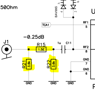
What is the purpose of this?
|
|
|
722
|
Mon Nov 5 17:17:08 2018 |
Sean Quinn | Pi attenuator on eval board inputs? | Dear DRS4 team,
I am curious about this part of the circuit:
What is the purpose of this? |
|
721
|
Wed Sep 26 19:21:03 2018 |
Stefan Ritt | Trigger OUT pulse width variable from 100 us up to 100 ms | In meantime I even updated the manual.
Stefan
| Gerard Arino-Estrada wrote: |
|
Thank you very much for the answer, I really appreciate your help.
Thanks!
Gerard
|
|
|
720
|
Wed Sep 26 18:28:20 2018 |
Gerard Arino-Estrada | Trigger OUT pulse width variable from 100 us up to 100 ms | Thank you very much for the answer, I really appreciate your help.
Thanks!
Gerard
| Stefan Ritt wrote: |
|
The "Trigger OUT" has changed recently. It goes high on a new trigger, but then STAYS high until the board has been read out by the PC and re-started. This allows better synchronization with some external trigger, which can be re-armed with the falling edge of the trigger out signal. The signal can be quite long, since readout of an event via USB typically takes 2 ms, but can be more if the PC is busy. If you need back your 150 ns pulse, send the trigger out to an external pulse shaper with fixed shaping width.
Stefan
| Gerard Arino-Estrada wrote: |
|
Hello Stefan,
I am using the DRS4 board connected to a Raspberry PI and through the drsosc application. I am interested on using the "Trigger OUT" signal to do some extra data processing with NIM modules. According to the manual, for each hardware trigger a TTL pulse of 150 ns width should be send through the "trigger OUT". In my case I do see pulses with widths ranging from 100 microseconds up to hundreds of miliseconds. I am connecting the signal directly to an oscilloscope with 50 Ohm termination. I have tried two DRS4 boards in identical conditions and both show the same behavior. Having such wide and variable pulses makes it complicated for me to do the extra post-processing. Have you any idea of what might be going wrong? Thank you very much.
Best regards,
Gerard
|
|
|
|
Draft
|
Wed Sep 26 18:25:07 2018 |
Gerard Arino-Estrada | Trigger OUT pulse width variable from 100 us up to 100 ms | Thank you very much for the answer, I really appreciate your help.
Thanks!
Gerard
| Stefan Ritt wrote: |
|
The "Trigger OUT" has changed recently. It goes high on a new trigger, but then STAYS high until the board has been read out by the PC and re-started. This allows better synchronization with some external trigger, which can be re-armed with the falling edge of the trigger out signal. The signal can be quite long, since readout of an event via USB typically takes 2 ms, but can be more if the PC is busy. If you need back your 150 ns pulse, send the trigger out to an external pulse shaper with fixed shaping width.
Stefan
| Gerard Arino-Estrada wrote: |
|
Hello Stefan,
I am using the DRS4 board connected to a Raspberry PI and through the drsosc application. I am interested on using the "Trigger OUT" signal to do some extra data processing with NIM modules. According to the manual, for each hardware trigger a TTL pulse of 150 ns width should be send through the "trigger OUT". In my case I do see pulses with widths ranging from 100 microseconds up to hundreds of miliseconds. I am connecting the signal directly to an oscilloscope with 50 Ohm termination. I have tried two DRS4 boards in identical conditions and both show the same behavior. Having such wide and variable pulses makes it complicated for me to do the extra post-processing. Have you any idea of what might be going wrong? Thank you very much.
Best regards,
Gerard
|
|
|
|
718
|
Wed Sep 26 14:44:14 2018 |
Stefan Ritt | Trigger OUT pulse width variable from 100 us up to 100 ms | The "Trigger OUT" has changed recently. It goes high on a new trigger, but then STAYS high until the board has been read out by the PC and re-started. This allows better synchronization with some external trigger, which can be re-armed with the falling edge of the trigger out signal. The signal can be quite long, since readout of an event via USB typically takes 2 ms, but can be more if the PC is busy. If you need back your 150 ns pulse, send the trigger out to an external pulse shaper with fixed shaping width.
Stefan
| Gerard Arino-Estrada wrote: |
|
Hello Stefan,
I am using the DRS4 board connected to a Raspberry PI and through the drsosc application. I am interested on using the "Trigger OUT" signal to do some extra data processing with NIM modules. According to the manual, for each hardware trigger a TTL pulse of 150 ns width should be send through the "trigger OUT". In my case I do see pulses with widths ranging from 100 microseconds up to hundreds of miliseconds. I am connecting the signal directly to an oscilloscope with 50 Ohm termination. I have tried two DRS4 boards in identical conditions and both show the same behavior. Having such wide and variable pulses makes it complicated for me to do the extra post-processing. Have you any idea of what might be going wrong? Thank you very much.
Best regards,
Gerard
|
|
|
717
|
Sun Sep 23 02:22:46 2018 |
Gerard Arino-Estrada | Trigger OUT pulse width variable from 100 us up to 100 ms | Hello Stefan,
I am using the DRS4 board connected to a Raspberry PI and through the drsosc application. I am interested on using the "Trigger OUT" signal to do some extra data processing with NIM modules. According to the manual, for each hardware trigger a TTL pulse of 150 ns width should be send through the "trigger OUT". In my case I do see pulses with widths ranging from 100 microseconds up to hundreds of miliseconds. I am connecting the signal directly to an oscilloscope with 50 Ohm termination. I have tried two DRS4 boards in identical conditions and both show the same behavior. Having such wide and variable pulses makes it complicated for me to do the extra post-processing. Have you any idea of what might be going wrong? Thank you very much.
Best regards,
Gerard |
|
716
|
Thu Sep 13 18:09:13 2018 |
Martin Petriska | "Symmetric spikes" fixed | Ok, so I made it ... and Yes it works :),
https://youtu.be/0noy4CoFoh8
here is changed part in drs4_eval4_app.vhd
        when done =>

          drs_readout_state    <= spikeoff;

          drs_stat_busy        <= '0';

          drs_dpram_we1        <= '0';

          drs_write_set        <= '1';   -- set drs_write_ff in proc_drs_write

                                         -- to keep chip "warm"
 -- spike fix ELOG 697


          when spikeoff =>

            o_drs_addr       <= "1011"; -- Address the read shift register by applying 1011b to A3:A0

            o_drs_srin       <= '0'; -- Switch SRIN low

             drs_readout_state                 <= spikecycle;

             -- Apply 1024 clock cycles to SRCLK

             drs_sr_count         <= 0;
          when spikecycle =>

             drs_sr_count         <= drs_sr_count + 1;

             o_drs_srclk          <= not o_drs_srclk;

             if (drs_sr_count = 1024) then

                drs_readout_state <= idle;

             end if;
-- set-up of configuration register
| Stefan Ritt wrote: |
|
Yes it's possible, but I have to find time for that. The software of the evaluation board takes care of the spikes ("remove spikes"), so I thought it's not so urgent to fix that in the FPGA (which takes me some time).
Stefan
| Martin Petriska wrote: |
|
Hi,
Is it possible to fix it by FPGA changes? I see readout cycle (proc_drs_reedout) in drs4_eval(4)5_app.vhd, but not sure where to exactly put this three commands. Could you please attach app.vhd file for eval board with example how to fix ?
Regards,
Martin
| Stefan Ritt wrote: |
|
Good news for all DRS4 users. After many years, I finally understand where the "symmetric spikes" come from and how to fix them.
The "symmetric spikes" are small spikes of 17-18mV, which randomly happen at 1-2 cells. They alwas come in groups of 2 in each channel, symmetric around sampling cell #512. See first attachment.
The reason for the spikes is the previous readout cycle. On each readout cycle, the "read bit" is clocked through all 1024 cells to switch one cell contents to the DRS4 output. At the end of the 1024 cycles, the read bit stays at its last position. The bit is carried by a metal line on the chip, which crosses all 9 channels (second attachment). This bit now influences the sampling cells below the metal line capacitively, so their contents is "pushed up" by a few mV, just like the ROFS offset does. Since the DRS sampling channels are in a snake layout, going 0-512 from left, then 512-1023 back again, the line crosses two cells in each channel, and thus the symmetric spikes.
Previously, there was a software solution for that. In the evaluation board software DRSOsc there is a button "Remove spikes" which tries to fix this in software. Although this works most of the time, it's annoying and not 100% safe. Like when the spike sits on top of a noise signal, it might not be recognized. Fixing this in hardware is however straight forwar. After the readout cycle ends, push the read bit out of the chip:
- Address the read shift register by applying 1011b to A3:A0
- Switch SRIN low
- Apply 1024 clock cycles to SRCLK
This shifts the bit out of the chip, so that the next event is not affected by the read bit. The third attachment show the effect of this. The "clear cycle" increases the readout time a little bit, but depending on the application this might be worth it.
Regards,
Stefan
|
|
|
|
|
715
|
Tue Sep 4 13:04:30 2018 |
Stefan Ritt | "Symmetric spikes" fixed | Yes it's possible, but I have to find time for that. The software of the evaluation board takes care of the spikes ("remove spikes"), so I thought it's not so urgent to fix that in the FPGA (which takes me some time).
Stefan
| Martin Petriska wrote: |
|
Hi,
Is it possible to fix it by FPGA changes? I see readout cycle (proc_drs_reedout) in drs4_eval(4)5_app.vhd, but not sure where to exactly put this three commands. Could you please attach app.vhd file for eval board with example how to fix ?
Regards,
Martin
| Stefan Ritt wrote: |
|
Good news for all DRS4 users. After many years, I finally understand where the "symmetric spikes" come from and how to fix them.
The "symmetric spikes" are small spikes of 17-18mV, which randomly happen at 1-2 cells. They alwas come in groups of 2 in each channel, symmetric around sampling cell #512. See first attachment.
The reason for the spikes is the previous readout cycle. On each readout cycle, the "read bit" is clocked through all 1024 cells to switch one cell contents to the DRS4 output. At the end of the 1024 cycles, the read bit stays at its last position. The bit is carried by a metal line on the chip, which crosses all 9 channels (second attachment). This bit now influences the sampling cells below the metal line capacitively, so their contents is "pushed up" by a few mV, just like the ROFS offset does. Since the DRS sampling channels are in a snake layout, going 0-512 from left, then 512-1023 back again, the line crosses two cells in each channel, and thus the symmetric spikes.
Previously, there was a software solution for that. In the evaluation board software DRSOsc there is a button "Remove spikes" which tries to fix this in software. Although this works most of the time, it's annoying and not 100% safe. Like when the spike sits on top of a noise signal, it might not be recognized. Fixing this in hardware is however straight forwar. After the readout cycle ends, push the read bit out of the chip:
- Address the read shift register by applying 1011b to A3:A0
- Switch SRIN low
- Apply 1024 clock cycles to SRCLK
This shifts the bit out of the chip, so that the next event is not affected by the read bit. The third attachment show the effect of this. The "clear cycle" increases the readout time a little bit, but depending on the application this might be worth it.
Regards,
Stefan
|
|
|
|
714
|
Mon Sep 3 11:17:26 2018 |
Martin Petriska | "Symmetric spikes" fixed | Hi,
Is it possible to fix it by FPGA changes? I see readout cycle (proc_drs_reedout) in drs4_eval(4)5_app.vhd, but not sure where to exactly put this three commands. Could you please attach app.vhd file for eval board with example how to fix ?
Regards,
Martin
| Stefan Ritt wrote: |
|
Good news for all DRS4 users. After many years, I finally understand where the "symmetric spikes" come from and how to fix them.
The "symmetric spikes" are small spikes of 17-18mV, which randomly happen at 1-2 cells. They alwas come in groups of 2 in each channel, symmetric around sampling cell #512. See first attachment.
The reason for the spikes is the previous readout cycle. On each readout cycle, the "read bit" is clocked through all 1024 cells to switch one cell contents to the DRS4 output. At the end of the 1024 cycles, the read bit stays at its last position. The bit is carried by a metal line on the chip, which crosses all 9 channels (second attachment). This bit now influences the sampling cells below the metal line capacitively, so their contents is "pushed up" by a few mV, just like the ROFS offset does. Since the DRS sampling channels are in a snake layout, going 0-512 from left, then 512-1023 back again, the line crosses two cells in each channel, and thus the symmetric spikes.
Previously, there was a software solution for that. In the evaluation board software DRSOsc there is a button "Remove spikes" which tries to fix this in software. Although this works most of the time, it's annoying and not 100% safe. Like when the spike sits on top of a noise signal, it might not be recognized. Fixing this in hardware is however straight forwar. After the readout cycle ends, push the read bit out of the chip:
- Address the read shift register by applying 1011b to A3:A0
- Switch SRIN low
- Apply 1024 clock cycles to SRCLK
This shifts the bit out of the chip, so that the next event is not affected by the read bit. The third attachment show the effect of this. The "clear cycle" increases the readout time a little bit, but depending on the application this might be worth it.
Regards,
Stefan
|
|
|
713
|
Tue Aug 21 14:36:44 2018 |
Stefan Ritt | Optimal readout speed | The analog output of the DRS4 chip needs some time to settle. In principle it need an infinite amout of time (exponential curve) to settle to 100% of the final value. So if we sample after a finite time, there is some error we do. Some of the error will be taken care of the voltage calibration, but there remains some residual error depending on the value of the previous sampling cell. So all sampling speeds 10 MHz, 16 MHz, 33 MHz are kind of rule of thumbs. In the end we run the evaluation board at 16 MHz to save a little bit of power (which is limited on an USB device). But I never made a careful study of noise-after-calibration vs. sampling speed. If you have some measurements, I'm happt to include it in the data sheet.
Stefan
| Sean Quinn wrote: |
|
Dear DRS4 team,
On page 3 of the data sheet, Table 1. for readout speed a typical value of 10 MHz is specified, but in the comment column it notes optimal performance achieved at 33 MHz.
I see the V5.1 eval board runs at 16 MHz. I'd like to understand the rationale for this using speed, instead of 33 MHz. Is there an SNR issue for the ADC at the higher speed, even though this is optimal for the DRS4?
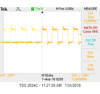
Very best,
Sean
|
|
|
712
|
Tue Aug 14 06:10:49 2018 |
Stefan Ritt | Latch delay support | I put that on the wish list, but I won't have time for that in the next months.
Stefan
| Martin Petriska wrote: |
|
Hi,
https://forge.physik.rwth-aachen.de/projects/drs4-rwth
Not sure about their licensing, but is it possible to add latch delay support to official firmware ?
Best regards
Martin
|
|
|
711
|
Mon Aug 13 19:44:59 2018 |
Martin Petriska | Latch delay support | Hi,
https://forge.physik.rwth-aachen.de/projects/drs4-rwth
Not sure about their licensing, but is it possible to add latch delay support to official firmware ?
Best regards
Martin |
|
710
|
Wed Aug 1 00:49:30 2018 |
Sean Quinn | Optimal readout speed | Dear DRS4 team,
On page 3 of the data sheet, Table 1. for readout speed a typical value of 10 MHz is specified, but in the comment column it notes optimal performance achieved at 33 MHz.
I see the V5.1 eval board runs at 16 MHz. I'd like to understand the rationale for this using speed, instead of 33 MHz. Is there an SNR issue for the ADC at the higher speed, even though this is optimal for the DRS4?
Very best,
Sean |
|
709
|
Fri Jul 20 00:44:13 2018 |
Woon-Seng Choong | Effect of interpolation on timing | Just a follow-up update.
It turns out that I was using a cubic spline interpolation with smoothing. If I required the cubic spline to go through the sampled points, then I obtained similar time resolution as the simple linear interpolation.
| Woon-Seng Choong wrote: |
|
Using a test pulse split into two channels of the DRS4 Evaluation Board v5, I looked at the time resolution using a leading edge threshold. The voltage and timing calibration was performed. One method (1) is to linearly interpolate between two points of the raw waveform that is above and below the threshold (this is exactly the algorithm given in read_binary.c in the drs4 source distribution); and another (2) is to use a cubic spline interpolation of the raw waveform. The results I obtained are:
Method 1: dt = 1.298 ns +/- 7.22 ps
Method 2: dt = 1.293 ns +/- 15.48 ps
I am really puzzled why the time resolution of the spline interpolation is about a factor 2 worse than the simple linear interpolation. Has anyone studied the time resolution using similar or other interpolation methods?
|
|
|
708
|
Mon Jul 16 19:39:35 2018 |
Woon-Seng Choong | Effect of interpolation on timing | Using a test pulse split into two channels of the DRS4 Evaluation Board v5, I looked at the time resolution using a leading edge threshold. The voltage and timing calibration was performed. One method (1) is to linearly interpolate between two points of the raw waveform that is above and below the threshold (this is exactly the algorithm given in read_binary.c in the drs4 source distribution); and another (2) is to use a cubic spline interpolation of the raw waveform. The results I obtained are:
Method 1: dt = 1.298 ns +/- 7.22 ps
Method 2: dt = 1.293 ns +/- 15.48 ps
I am really puzzled why the time resolution of the spline interpolation is about a factor 2 worse than the simple linear interpolation. Has anyone studied the time resolution using similar or other interpolation methods?
|
|
707
|
Fri Jun 29 07:51:33 2018 |
Stefan Ritt | Negative Bin Width | Yes that's normal. A negative cell bin width means that the next cell N+1 samples the input signal before cell N. This can happen due to the signal routing on the DRS4 chip.
Stefan
| Woon-Seng Choong wrote: |
|
I am using a DRS4 Evaluation Board v5 and running the drsosc.exe version 5.06 on a Window 7 machine. I have performed the voltage and timing calibration.
With test pulses on channel 1 and 2, I collected binary data file with all 4 channels active sampling at 5GSPS.
Attached is a distribution of the bin_width vs. cell # for all the 4 channels. Note that there are few cells with bin_width < 10 ps.
Channel 1: bin_width[498] = -0.000348, bin_width[1010]= -0.000348
Channel 2: bin_width[498] = 0.007363
Channel 3: bin_width[498] = 0.007843
Channel 4: bin_width[498] = 0.005948
Is this normal? How can you get negative bin_width? What does negative bin_width means?
I have attached the binary data file for your verification.
|
|
|
706
|
Thu Jun 28 19:55:45 2018 |
Woon-Seng Choong | Negative Bin Width | I am using a DRS4 Evaluation Board v5 and running the drsosc.exe version 5.06 on a Window 7 machine. I have performed the voltage and timing calibration.
With test pulses on channel 1 and 2, I collected binary data file with all 4 channels active sampling at 5GSPS.
Attached is a distribution of the bin_width vs. cell # for all the 4 channels. Note that there are few cells with bin_width < 10 ps.
Channel 1: bin_width[498] = -0.000348, bin_width[1010]= -0.000348
Channel 2: bin_width[498] = 0.007363
Channel 3: bin_width[498] = 0.007843
Channel 4: bin_width[498] = 0.005948
Is this normal? How can you get negative bin_width? What does negative bin_width means?
I have attached the binary data file for your verification.
|
| Attachment 1: bin_width_5gsps.jpg
|

|
| Attachment 2: test5gsps.dat
|
|
705
|
Tue Jun 19 12:54:51 2018 |
Phan Van Chuan | The data acquisition speed | Thank Stefan Ritt, I added the SoftTrigger() just after StartDomino(), so now, The data acquisition speed the same speed as in the DRS oscilloscope. I have misunderstood the "auto" trigger on an oscilloscope as setting SetTriggerLevel (0).
Thank so much!
Phan Van Chuan
| Phan Van Chuan wrote: |
|
Dear Stefan,
We are using an DRS4 board V5.1 for building a metering system for the scintillator detector by a Labview program. The program was built based on the functions in DRS.cpp and it reads data from channel 0 very well (Fig 1). Now, I am having a problem with the data acquisition from DRS4 board. The data acquisition speed on this program is only about 30-50 Acq / s, while using the DRS Oscilloscope that of about 300-400 Acq / s.
When the program was installed with fDominoMode = 0 and fDominoActive = 0, the data acquisition speed was about 300-400 Acq / s. However, the waveform is inaccurate.
I do not know if I installed the wrong function! Can you show me how to solve this problem?
In the Labview program, functions (corresponding to functions in DRS.cpp) are called with the following parameters:
InitFPGA();
SetMultiBuffer(0);
fROFS = 1.6; // differential input range -0.5V ... +0.5V
fRange = 0;
SetDAC(fDAC_ROFS_1, fROFS);
fCommonMode = 0.8; // 0.8V +- 0.5V inside NMOS range
SetDAC(fDAC_CALP, fCommonMode);
SetDAC(fDAC_CALN, fCommonMode);
SetDAC(fDAC_BIAS, 0.70);
/* set default number of channels per chip */
SetChannelConfig(0, fNumberOfReadoutChannels - 1, 8);
// set ADC clock phase
fADCClkPhase = 0;
fADCClkInvert = 0;
// default settings
fMultiBuffer = 0;
fNMultiBuffer = 0;
fDominoMode = 1;
fReadoutMode = 1;
fReadPointer = 0;
fTriggerEnable1 = 1;
fTriggerEnable2 = 0;
fTriggerSource = 0;
fTriggerDelay = 0;
fTriggerDelayNs = 0;
fSyncDelay = 0;
fNominalFrequency = 1;
fDominoActive = 1;
// load calibration from EEPROM
ReadCalibration();
...
SetDominoMode(fDominoMode);
SetReadoutMode(fReadoutMode);
EnableTrigger(fTriggerEnable1, fTriggerEnable2);
SetTriggerSource(fTriggerSource);
SetTriggerDelayPercent(0);
SetSyncDelay(fSyncDelay);
SetDominoActive(fDominoActive);
SetFrequency(fNominalFrequency, true);
SetInputRange(fRange);
SelectClockSource(0); // FPGA clock
// disable calibration signals
EnableAcal(0, 0);
SetCalibTiming(0, 0);
EnableTcal(0);
// got to idle state
Reinit();
////////
SetFrequency (1,false);
settranspmode (1);
setinputrange(0);
EnableTcal (0,-,-);
EnableTrigger(1, 0);
SetTriggerSource(0);
SetTriggerLevel(0);
SetTriggerPolarity(false);
SetTriggerDelayNs(512);
// in loop of read data from DRS4:
{
StartDomino();
while (b->IsBusy());
TransferWaves(0, 8);
GetTime(0, 0, b->GetTriggerCell(0), time_array[0]);
GetWave(0, 0, wave_array[0]);
}
Thank you very much!
Best Regards,
Chuan
|
|
|
704
|
Tue Jun 19 10:05:50 2018 |
Stefan Ritt | The data acquisition speed | How do you tigger the board? In your code below you start the board (StartDomino()) and then wait for a trigger. Setting the trigger level to zero (via SetTriggerLevel(0)) is certainly wrong. Please have a look at drs_exam.cpp in the distribution and use the same functions used there. If you want to trigger the board, you need some external pulser with high enough rate (more than 500 Hz or course). You can also "software" trigger the board with a call to SoftTrigger() just after StartDomino(). This is then like the "auto" trigger on an oscilloscope.
Stefan
| Phan Van Chuan wrote: |
|
Dear Stefan,
We are using an DRS4 board V5.1 for building a metering system for the scintillator detector by a Labview program. The program was built based on the functions in DRS.cpp and it reads data from channel 0 very well (Fig 1). Now, I am having a problem with the data acquisition from DRS4 board. The data acquisition speed on this program is only about 30-50 Acq / s, while using the DRS Oscilloscope that of about 300-400 Acq / s.
When the program was installed with fDominoMode = 0 and fDominoActive = 0, the data acquisition speed was about 300-400 Acq / s. However, the waveform is inaccurate.
I do not know if I installed the wrong function! Can you show me how to solve this problem?
In the Labview program, functions (corresponding to functions in DRS.cpp) are called with the following parameters:
InitFPGA();
SetMultiBuffer(0);
fROFS = 1.6; // differential input range -0.5V ... +0.5V
fRange = 0;
SetDAC(fDAC_ROFS_1, fROFS);
fCommonMode = 0.8; // 0.8V +- 0.5V inside NMOS range
SetDAC(fDAC_CALP, fCommonMode);
SetDAC(fDAC_CALN, fCommonMode);
SetDAC(fDAC_BIAS, 0.70);
/* set default number of channels per chip */
SetChannelConfig(0, fNumberOfReadoutChannels - 1, 8);
// set ADC clock phase
fADCClkPhase = 0;
fADCClkInvert = 0;
// default settings
fMultiBuffer = 0;
fNMultiBuffer = 0;
fDominoMode = 1;
fReadoutMode = 1;
fReadPointer = 0;
fTriggerEnable1 = 1;
fTriggerEnable2 = 0;
fTriggerSource = 0;
fTriggerDelay = 0;
fTriggerDelayNs = 0;
fSyncDelay = 0;
fNominalFrequency = 1;
fDominoActive = 1;
// load calibration from EEPROM
ReadCalibration();
...
SetDominoMode(fDominoMode);
SetReadoutMode(fReadoutMode);
EnableTrigger(fTriggerEnable1, fTriggerEnable2);
SetTriggerSource(fTriggerSource);
SetTriggerDelayPercent(0);
SetSyncDelay(fSyncDelay);
SetDominoActive(fDominoActive);
SetFrequency(fNominalFrequency, true);
SetInputRange(fRange);
SelectClockSource(0); // FPGA clock
// disable calibration signals
EnableAcal(0, 0);
SetCalibTiming(0, 0);
EnableTcal(0);
// got to idle state
Reinit();
////////
SetFrequency (1,false);
settranspmode (1);
setinputrange(0);
EnableTcal (0,-,-);
EnableTrigger(1, 0);
SetTriggerSource(0);
SetTriggerLevel(0);
SetTriggerPolarity(false);
SetTriggerDelayNs(512);
// in loop of read data from DRS4:
{
StartDomino();
while (b->IsBusy());
TransferWaves(0, 8);
GetTime(0, 0, b->GetTriggerCell(0), time_array[0]);
GetWave(0, 0, wave_array[0]);
}
Thank you very much!
Best Regards,
Chuan
|
|
|
703
|
Tue Jun 19 06:42:23 2018 |
Phan Van Chuan | The data acquisition speed | Dear Stefan,
We are using an DRS4 board V5.1 for building a metering system for the scintillator detector by a Labview program. The program was built based on the functions in DRS.cpp and it reads data from channel 0 very well (Fig 1). Now, I am having a problem with the data acquisition from DRS4 board. The data acquisition speed on this program is only about 30-50 Acq / s, while using the DRS Oscilloscope that of about 300-400 Acq / s.
When the program was installed with fDominoMode = 0 and fDominoActive = 0, the data acquisition speed was about 300-400 Acq / s. However, the waveform is inaccurate.
I do not know if I installed the wrong function! Can you show me how to solve this problem?
In the Labview program, functions (corresponding to functions in DRS.cpp) are called with the following parameters:
InitFPGA();
SetMultiBuffer(0);
fROFS = 1.6; // differential input range -0.5V ... +0.5V
fRange = 0;
SetDAC(fDAC_ROFS_1, fROFS);
fCommonMode = 0.8; // 0.8V +- 0.5V inside NMOS range
SetDAC(fDAC_CALP, fCommonMode);
SetDAC(fDAC_CALN, fCommonMode);
SetDAC(fDAC_BIAS, 0.70);
/* set default number of channels per chip */
SetChannelConfig(0, fNumberOfReadoutChannels - 1, 8);
// set ADC clock phase
fADCClkPhase = 0;
fADCClkInvert = 0;
// default settings
fMultiBuffer = 0;
fNMultiBuffer = 0;
fDominoMode = 1;
fReadoutMode = 1;
fReadPointer = 0;
fTriggerEnable1 = 1;
fTriggerEnable2 = 0;
fTriggerSource = 0;
fTriggerDelay = 0;
fTriggerDelayNs = 0;
fSyncDelay = 0;
fNominalFrequency = 1;
fDominoActive = 1;
// load calibration from EEPROM
ReadCalibration();
...
SetDominoMode(fDominoMode);
SetReadoutMode(fReadoutMode);
EnableTrigger(fTriggerEnable1, fTriggerEnable2);
SetTriggerSource(fTriggerSource);
SetTriggerDelayPercent(0);
SetSyncDelay(fSyncDelay);
SetDominoActive(fDominoActive);
SetFrequency(fNominalFrequency, true);
SetInputRange(fRange);
SelectClockSource(0); // FPGA clock
// disable calibration signals
EnableAcal(0, 0);
SetCalibTiming(0, 0);
EnableTcal(0);
// got to idle state
Reinit();
////////
SetFrequency (1,false);
settranspmode (1);
setinputrange(0);
EnableTcal (0,-,-);
EnableTrigger(1, 0);
SetTriggerSource(0);
SetTriggerLevel(0);
SetTriggerPolarity(false);
SetTriggerDelayNs(512);
// in loop of read data from DRS4:
{
StartDomino();
while (b->IsBusy());
TransferWaves(0, 8);
GetTime(0, 0, b->GetTriggerCell(0), time_array[0]);
GetWave(0, 0, wave_array[0]);
}
Thank you very much!
Best Regards,
Chuan
|
| Attachment 1: wavech0.png
|

|
|
702
|
Wed Jun 13 16:34:28 2018 |
Julian Kemp | Maximum analog input voltage | Thank you! That solves my problem.
| Stefan Ritt wrote: |
|
In principle the numbers in the manual are correct. But they relate to pulses of a certain length, because the input protection only works for DC voltage and for pulses which are not too long. Since we could not write this all on the label of the board, we decided to put there 100% safe value as a "warning" to people, meaning that if pulses are above 2.5V, they should look into the manual and read the details.
Stefan
| Julian Kemp wrote: |
|
Dear all,
I have been wondering what the maximum analog input voltage for the DRS4 V5 evaluation board is. It came with a sticker indicating that it is "2.5V pk Max". On the other hand, when checking the manual (https://www.psi.ch/drs/DocumentationEN/manual_rev50.pdf), it says maximum allowed is 10V DC or even 30V for short pulses. I foresee an application where I cannot make sure that pulses stay below 2.5V, so the correct value will be quite important for me.
Best,
Julian
|
|
|
|
701
|
Wed Jun 13 13:42:47 2018 |
Stefan Ritt | Maximum analog input voltage | In principle the numbers in the manual are correct. But they relate to pulses of a certain length, because the input protection only works for DC voltage and for pulses which are not too long. Since we could not write this all on the label of the board, we decided to put there 100% safe value as a "warning" to people, meaning that if pulses are above 2.5V, they should look into the manual and read the details.
Stefan
| Julian Kemp wrote: |
|
Dear all,
I have been wondering what the maximum analog input voltage for the DRS4 V5 evaluation board is. It came with a sticker indicating that it is "2.5V pk Max". On the other hand, when checking the manual (https://www.psi.ch/drs/DocumentationEN/manual_rev50.pdf), it says maximum allowed is 10V DC or even 30V for short pulses. I foresee an application where I cannot make sure that pulses stay below 2.5V, so the correct value will be quite important for me.
Best,
Julian
|
|
|
700
|
Wed Jun 13 13:23:17 2018 |
Julian Kemp | Maximum analog input voltage | Dear all,
I have been wondering what the maximum analog input voltage for the DRS4 V5 evaluation board is. It came with a sticker indicating that it is "2.5V pk Max". On the other hand, when checking the manual (https://www.psi.ch/drs/DocumentationEN/manual_rev50.pdf), it says maximum allowed is 10V DC or even 30V for short pulses. I foresee an application where I cannot make sure that pulses stay below 2.5V, so the correct value will be quite important for me.
Best,
Julian |
|
699
|
Fri Jun 8 08:11:05 2018 |
Stefan Ritt | | Several people reported this problem, but we cannot reproduce it at our lab. Both the oscilloscope and the command line interface use exactly the same code to connect to the board. Have you tried the solution reported here: elog:657 ?
Best,
Stefan
| Phan Van Chuan wrote: |
|
Dear Stefan,
I am using an DRS4 board to test the signal from an scintillator detector; It has connected well to the computer on DRS Oscilloscope (Figure 1). Now, I am having a problem of developing from the code of the drs_exam program, because the DRS4 board has not connected to the computer when translation the drs_exam program (Figure 2). Before running the drs_exam program, I copied the libusb-1.0.lib file to the computer's "C: \ Program Files \ Microsoft SDKs \ Windows \ v7.0A \ Lib" folder. Can you show me how to solve this problem?
Figure 1.
Figure 2.
Thank you very much!
Best Regards,
Chuan
|
|
|
698
|
Thu Jun 7 16:27:21 2018 |
Phan Van Chuan | | Dear Stefan,
I am using an DRS4 board to test the signal from an scintillator detector; It has connected well to the computer on DRS Oscilloscope (Figure 1). Now, I am having a problem of developing from the code of the drs_exam program, because the DRS4 board has not connected to the computer when translation the drs_exam program (Figure 2). Before running the drs_exam program, I copied the libusb-1.0.lib file to the computer's "C: \ Program Files \ Microsoft SDKs \ Windows \ v7.0A \ Lib" folder. Can you show me how to solve this problem?
Figure 1.
Figure 2.
Thank you very much!
Best Regards,
Chuan |
| Attachment 1: figure1.png
|

|
| Attachment 2: figure2.png
|

|
|
697
|
Thu May 17 13:29:34 2018 |
Stefan Ritt | "Symmetric spikes" fixed | Good news for all DRS4 users. After many years, I finally understand where the "symmetric spikes" come from and how to fix them.
The "symmetric spikes" are small spikes of 17-18mV, which randomly happen at 1-2 cells. They alwas come in groups of 2 in each channel, symmetric around sampling cell #512. See first attachment.
The reason for the spikes is the previous readout cycle. On each readout cycle, the "read bit" is clocked through all 1024 cells to switch one cell contents to the DRS4 output. At the end of the 1024 cycles, the read bit stays at its last position. The bit is carried by a metal line on the chip, which crosses all 9 channels (second attachment). This bit now influences the sampling cells below the metal line capacitively, so their contents is "pushed up" by a few mV, just like the ROFS offset does. Since the DRS sampling channels are in a snake layout, going 0-512 from left, then 512-1023 back again, the line crosses two cells in each channel, and thus the symmetric spikes.
Previously, there was a software solution for that. In the evaluation board software DRSOsc there is a button "Remove spikes" which tries to fix this in software. Although this works most of the time, it's annoying and not 100% safe. Like when the spike sits on top of a noise signal, it might not be recognized. Fixing this in hardware is however straight forwar. After the readout cycle ends, push the read bit out of the chip:
- Address the read shift register by applying 1011b to A3:A0
- Switch SRIN low
- Apply 1024 clock cycles to SRCLK
This shifts the bit out of the chip, so that the next event is not affected by the read bit. The third attachment show the effect of this. The "clear cycle" increases the readout time a little bit, but depending on the application this might be worth it.
Regards,
Stefan |
| Attachment 1: with.png
|

|
| Attachment 2: Screen_Shot_2018-05-17_at_13.30.23_.png
|

|
| Attachment 3: without.png
|

|
|
696
|
Mon May 14 09:21:29 2018 |
Alessio Berti | WIndows Connection problem with drs507 SOLVED | Hi,
I have a machine with Windows 10 and the solution provided by Steven works fine. To give more details, the driver installed in my case is WinUSB (i.e. libusb, v6.1.7600.16385).
Cheers,
Alessio
| Alec Shackleford wrote: |
|
Thank you for this fantastic solution. I had almost reinstalled windows 7 to see if that would solve the issue!
All the best,
Alec
| Stefan Ritt wrote: |
|
Dear Steven, many thanks for this information, this is very useful. I know of people having problems on Windows 10, maybe this will also help them.
Stefan
| Steven Block wrote: |
|
Hello All,
I too have been struggling with trying to get the drs4 (507) to work on my windows machine and I found it to be a problem with the libusb library. My solution is as follows and has worked on multiple PC's. I ran this solution after I first plugged in the drs4 and installed 507.
Go to http://zadig.akeo.ie/ and install the corresponding software.
After that, you will need to plug in the DRS4 to your computer. From there go to ‘Options’, and select ‘List all Devices’.
Finally, choose the DRS4 evaluation board from the list and press install driver and let it run. You should be fine after that.
Best,
Steven
|
|
|
|
|
695
|
Wed May 9 14:07:10 2018 |
Alec Shackleford | WIndows Connection problem with drs507 SOLVED | Thank you for this fantastic solution. I had almost reinstalled windows 7 to see if that would solve the issue!
All the best,
Alec
| Stefan Ritt wrote: |
|
Dear Steven, many thanks for this information, this is very useful. I know of people having problems on Windows 10, maybe this will also help them.
Stefan
| Steven Block wrote: |
|
Hello All,
I too have been struggling with trying to get the drs4 (507) to work on my windows machine and I found it to be a problem with the libusb library. My solution is as follows and has worked on multiple PC's. I ran this solution after I first plugged in the drs4 and installed 507.
Go to http://zadig.akeo.ie/ and install the corresponding software.
After that, you will need to plug in the DRS4 to your computer. From there go to ‘Options’, and select ‘List all Devices’.
Finally, choose the DRS4 evaluation board from the list and press install driver and let it run. You should be fine after that.
Best,
Steven
|
|
|
|
694
|
Wed May 9 09:03:52 2018 |
Stefan Ritt | Manual Rev5.1 Figure 1, optional components | I updated the picture in the manual with a current picture of a Rev5.1 board, and also added a picture of the bottom side. If you need a picture without the blue labels, have a look at https://www.psi.ch/drs/old-evaluation-boards at the bottom.
Here is the explanation of the optional components:
- R1, C2, R6, R29, R30 and same components for other channels: Normally the board is AC-coupled. You can make the board DC-coupled by briding C1, C9, C13, removing R6, C2, adding R1, adding R29, removing R30. The CAL signal then enters before the THS4508. We found that DC coupling gives slightly higher noise and is prone to high input DC levels, so we ship the board usually AC-coupled.
- R84 & Co. defines the hysteresis of the trigger comparators as described in the schematics
- R99-R106, R143: If soldered, the board is configured in cascading mode with 4 channels @ 2048 bins. R143 tells the FPGA that we are in this mode, so the firmware can correctly configure the DRS4
- R118 & Co. defines the MCX output level to be either 3.3V or 5V (default)
- R146-R149 connect JTAG to the uC. We planned at one point to make firmware upgrades through USB, but we never implemented that, so these resistors are not soldered.
I hope I covered everything. If I overlooked any optional component please tell me.
Cheers,
Stefan
| Sean Quinn wrote: |
|
Dear All,
I'm troubleshooting a board which uses the DRS4 and adopts an analog front end very similar to the evaluation board. As a result, we rely on the eval board as a reference. In doing so we've encountered an issue in the manual:
The high resolution photo in Figure 1. is useful, but it seems to correspond to an older version of the board. For instance, the RF switch can't correspond to the schematics of Rev5.1 in the appendix.
Request: Could the manual be updated with a high resolution image of Rev5.1. Also, could a high resolution of the bottom side of the board be included in the manual? This is desirable since it has the version number and contact information, so it will remove any ambiguity about what board you're looking at and what schematics you should refer to.
A second question, which might be overly broad: what is the impact of installing the optional components (marked * in the schematics) on the analog front end? Why are a lot of these left uninstalled on the eval board?
Thanks,
Sean
|
|
|
693
|
Tue May 8 23:58:35 2018 |
Sean Quinn | Manual Rev5.1 Figure 1, optional components | Dear All,
I'm troubleshooting a board which uses the DRS4 and adopts an analog front end very similar to the evaluation board. As a result, we rely on the eval board as a reference. In doing so we've encountered an issue in the manual:
The high resolution photo in Figure 1. is useful, but it seems to correspond to an older version of the board. For instance, the RF switch can't correspond to the schematics of Rev5.1 in the appendix.
Request: Could the manual be updated with a high resolution image of Rev5.1. Also, could a high resolution of the bottom side of the board be included in the manual? This is desirable since it has the version number and contact information, so it will remove any ambiguity about what board you're looking at and what schematics you should refer to.
A second question, which might be overly broad: what is the impact of installing the optional components (marked * in the schematics) on the analog front end? Why are a lot of these left uninstalled on the eval board?
Thanks,
Sean |
|
692
|
Tue May 8 14:43:03 2018 |
Stefan Ritt | Peak at 0 mV in traces | The DRS chip is read out with a 12 bit ADC, thus the phyical resolution is roughly 1V/4096 = 0.24 mV. I say roughly since the DRS has an analog gain of 0.98, which is corrected for. Now you have integer values which are converted into floating point numbers my multiplying them with ~0.24mV. If you then do histogramming with different bin sizes such as 0.1 mV and 0.35 mV , you get aliasing effects. The code truncates the result to 0.1 mV, which can give you also rounding artifacts. You will probalby see the same if you generate random 12 bit values and do the same histogramming. The 0.35 mV are not the RESOLUTION of the board (this is 0.24 mV as written above), but the Signal-To-Noise ratio of the DRS chip. If you measure zero volts at the input, and you make statistics over the distribution, you get an RMS of 0.35 mV.
Stefan
| Alessio Berti wrote: |
|
Hi Stefan,
following your example, we tried to perform the same measurement, using drs_exam and taking 1000 events. The results we obtained are in the plots attached (both in log and linear scale). We tried two different binnings:
- the first is the same as the one used in your example, that is 0.1 mV (corresponding to the plots having 81 bins)
- the second is a more wide binning equal to 0.35 mV, that is (2^(-11.5)) mV, 11.5 being the effective number of bits given in the DRS4 spreadsheet (corresponding to the plots having 23 bins)
With the fine binning we see that in the bin centered around 0 there is a little excess of events (the effect is more visible in the log scale histograms). This excess is not present in the wide binning case.
Is the problem we had before (and also here in the fine binning case) lying in the fact that we were trying to have bins with a width smaller than the effective resolution of the instrument (0.35 mV)?
We also noticed that in drs_exam, the values for the waveform are printed in the ASCII file with 1 digit after the decimal point, but when trying to print more digits the resolution is not improved (i.e. the decimal digits from the second one on are 0). This means that the values are rounded to a resolution of 0.1 mV when they are saved through the GetWave() routine (and in fact the member fPrecision is set to 0.1 -mV- in DRS.cpp, line 7502, and also in DRS.h, line 757, GetPrecision() returns 0.1). Why is that so? How does it reconcile with the effective number of bits giving a resolution of 0.35 mV?
Thank you,
Alessio & Davide
| Stefan Ritt wrote: |
|
I tried the following:
- trigger on a 10 MHz sine wave on CH0, CH1 was open
- run drs_exam.cpp program and write data.txt with a few events
- imported the event into Excel
- did a histogram on (empty) CH1
What I see is a nice Gaussian distribution centered around 1mV, but with no spike around zero. See attachment. So I still believe that you have either a binning or a rounding problem. Like you round value -0.99 to +0.99 all to zero mV, and 1.00 to 1.99 mV to one mV.
Stefan
| Alessio Berti wrote: |
|
Hi,
thank you for the quick reply. All the bins in the previous histograms have the same width. We also tried to plot the noise histogram for channel 2 with more bins (i.e. 1000, so that we can see almost discrete values), and the peak is still there.
Alessio & Davide
| Stefan Ritt wrote: |
|
I note that your peak at zero is exactly twice as high as the bins left and right, so this looks to me like a binning problem in your histogramming. Maybe your bin #0 goes from -1mV to +1mV, which all other bins are just 1mW wide. Can you check that?
Stefan
| Alessio Berti wrote: |
|
Hi,
we modified drs_exam.cpp to read all 4 channels from the DRS4 and apply directly the spike removal (taken from Osci.cpp) during the acquisition phase. For test purposes, we don't save the data showing spikes and we focus on the data not having spikes (even if at the end we end up having triple and quadro spikes which are not removed by the spike removal routine, but they are rare). With this modified program we wanted to characterize the noise of the DRS4, so we took 30000 events at 5GSPS, triggering on channel 1 with a 10 MHz sine wave with 100 mV_pp (trigger level set at 10 mV), while channels 2,3 and 4 were left open without any input.
We then took a look at the data and plotted the noise histograms for channels 2,3 and 4, which you can find attached (without offset correction, named zero_peak_after_spike_removal_ch*.png). For completeness, we also attached the plot from ch1 (the sine wave). The selections in time and amplitude we applied had the goal to remove the high oscillations in amplitude occurring in the first and last samples and to discard the quadro spikes we had in the data.
We see that there is a peak at 0 mV in all histograms from all channels and scanning through the data, we saw that indeed the value 0 mV is stored many times for each event, thus originating the peak we see in the histograms. We also applied an offset correction to the data (taking the average of the first three most occuring amplitudes) of channels 2 (as an example) and the problem seems to be only partially removed.
We also noticed that this peak at 0 mV is present also when we acquired the data from the DRS4 with DRSosc saving the data in binary format.
So we had the following questions:
- why is the DRS4 saving so many times the value 0 mV (exactly 0 mV)?
- is there any way (in our case through software, preferably at acquisition time) to solve this problem?
Thank you for the help and best regards,
Alessio & Davide
|
|
|
|
|
|
|
691
|
Tue May 8 12:15:54 2018 |
Alessio Berti | Peak at 0 mV in traces | Hi Stefan,
following your example, we tried to perform the same measurement, using drs_exam and taking 1000 events. The results we obtained are in the plots attached (both in log and linear scale). We tried two different binnings:
- the first is the same as the one used in your example, that is 0.1 mV (corresponding to the plots having 81 bins)
- the second is a more wide binning equal to 0.35 mV, that is (2^(-11.5)) mV, 11.5 being the effective number of bits given in the DRS4 spreadsheet (corresponding to the plots having 23 bins)
With the fine binning we see that in the bin centered around 0 there is a little excess of events (the effect is more visible in the log scale histograms). This excess is not present in the wide binning case.
Is the problem we had before (and also here in the fine binning case) lying in the fact that we were trying to have bins with a width smaller than the effective resolution of the instrument (0.35 mV)?
We also noticed that in drs_exam, the values for the waveform are printed in the ASCII file with 1 digit after the decimal point, but when trying to print more digits the resolution is not improved (i.e. the decimal digits from the second one on are 0). This means that the values are rounded to a resolution of 0.1 mV when they are saved through the GetWave() routine (and in fact the member fPrecision is set to 0.1 -mV- in DRS.cpp, line 7502, and also in DRS.h, line 757, GetPrecision() returns 0.1). Why is that so? How does it reconcile with the effective number of bits giving a resolution of 0.35 mV?
Thank you,
Alessio & Davide
| Stefan Ritt wrote: |
|
I tried the following:
- trigger on a 10 MHz sine wave on CH0, CH1 was open
- run drs_exam.cpp program and write data.txt with a few events
- imported the event into Excel
- did a histogram on (empty) CH1
What I see is a nice Gaussian distribution centered around 1mV, but with no spike around zero. See attachment. So I still believe that you have either a binning or a rounding problem. Like you round value -0.99 to +0.99 all to zero mV, and 1.00 to 1.99 mV to one mV.
Stefan
| Alessio Berti wrote: |
|
Hi,
thank you for the quick reply. All the bins in the previous histograms have the same width. We also tried to plot the noise histogram for channel 2 with more bins (i.e. 1000, so that we can see almost discrete values), and the peak is still there.
Alessio & Davide
| Stefan Ritt wrote: |
|
I note that your peak at zero is exactly twice as high as the bins left and right, so this looks to me like a binning problem in your histogramming. Maybe your bin #0 goes from -1mV to +1mV, which all other bins are just 1mW wide. Can you check that?
Stefan
| Alessio Berti wrote: |
|
Hi,
we modified drs_exam.cpp to read all 4 channels from the DRS4 and apply directly the spike removal (taken from Osci.cpp) during the acquisition phase. For test purposes, we don't save the data showing spikes and we focus on the data not having spikes (even if at the end we end up having triple and quadro spikes which are not removed by the spike removal routine, but they are rare). With this modified program we wanted to characterize the noise of the DRS4, so we took 30000 events at 5GSPS, triggering on channel 1 with a 10 MHz sine wave with 100 mV_pp (trigger level set at 10 mV), while channels 2,3 and 4 were left open without any input.
We then took a look at the data and plotted the noise histograms for channels 2,3 and 4, which you can find attached (without offset correction, named zero_peak_after_spike_removal_ch*.png). For completeness, we also attached the plot from ch1 (the sine wave). The selections in time and amplitude we applied had the goal to remove the high oscillations in amplitude occurring in the first and last samples and to discard the quadro spikes we had in the data.
We see that there is a peak at 0 mV in all histograms from all channels and scanning through the data, we saw that indeed the value 0 mV is stored many times for each event, thus originating the peak we see in the histograms. We also applied an offset correction to the data (taking the average of the first three most occuring amplitudes) of channels 2 (as an example) and the problem seems to be only partially removed.
We also noticed that this peak at 0 mV is present also when we acquired the data from the DRS4 with DRSosc saving the data in binary format.
So we had the following questions:
- why is the DRS4 saving so many times the value 0 mV (exactly 0 mV)?
- is there any way (in our case through software, preferably at acquisition time) to solve this problem?
Thank you for the help and best regards,
Alessio & Davide
|
|
|
|
|
| Attachment 1: 20180508_drs4_drs_exam_1000_events_81_bins_linear.png
|

|
| Attachment 2: 20180508_drs4_drs_exam_1000_events_81_bins_log.png
|

|
| Attachment 3: 20180508_drs4_drs_exam_1000_events_23_bins_linear.png
|

|
| Attachment 4: 20180508_drs4_drs_exam_1000_events_23_bins_log.png
|

|
|
690
|
Sun May 6 11:45:09 2018 |
Stefan Ritt | confusion about the description in drs.cpp | The locbus_addr is indeed 32 bits wide, since the firmware was originally derived from some firmware running in a VME crate, and the VME bus has 32 bits or addressing. So you will still find some "historic" remnants from that era. In the USB firmware, lcobus_addr[32:8] is always zero. Sorry for the confusuion.
Stefan
| chen wenjun wrote: |
|
Hi Stefan:
I'm still confused that althought the 8 bits buffer is enough,the FPGA receive the command through the uc_data_i register which is 16 bits wides.As we can see in the firmware, the locbus_addr is 32 bits wides. Does it means the locbus_addr[31:8] are always '0' because the address in buffer is only 8 bits. Does it means the usrbus_status_sel and usrbus_ram_sel are also '0' all the time .
thanks!
chen
| Stefan Ritt wrote: |
|
The FPGA is very small, so it only has an address space of 256 bytes. Look at the definition in DRS.cpp
#define USB_CTRL_OFFSET 0x00 /* all registers 32 bit */
#define USB_STATUS_OFFSET 0x40
#define USB_RAM_OFFSET 0x80
The registers are 32 bits wide, but the addresses only run from 0 to 255, and thus a single byte is enough for addressing them.
| chen wenjun wrote: |
|
Hi,Stefan:
recently,whtn I study the drs.cpp code ,I found that the buffer[1] is char but the addr and the base_addr are all unsigned int,isn't there any problem that the addr may be cut off to 8 bits? Also ,I found that the data fpga recieved from the usb is 16 bits,so how can fpga get the true 32bits address from the PC.
|
|
|
|
|
689
|
Sun May 6 08:13:37 2018 |
chen wenjun | confusion about the description in drs.cpp | Hi Stefan:
I'm still confused that althought the 8 bits buffer is enough,the FPGA receive the command through the uc_data_i register which is 16 bits wides.As we can see in the firmware, the locbus_addr is 32 bits wides. Does it means the locbus_addr[31:8] are always '0' because the address in buffer is only 8 bits. Does it means the usrbus_status_sel and usrbus_ram_sel are also '0' all the time .
thanks!
chen
| Stefan Ritt wrote: |
|
The FPGA is very small, so it only has an address space of 256 bytes. Look at the definition in DRS.cpp
#define USB_CTRL_OFFSET 0x00 /* all registers 32 bit */
#define USB_STATUS_OFFSET 0x40
#define USB_RAM_OFFSET 0x80
The registers are 32 bits wide, but the addresses only run from 0 to 255, and thus a single byte is enough for addressing them.
| chen wenjun wrote: |
|
Hi,Stefan:
recently,whtn I study the drs.cpp code ,I found that the buffer[1] is char but the addr and the base_addr are all unsigned int,isn't there any problem that the addr may be cut off to 8 bits? Also ,I found that the data fpga recieved from the usb is 16 bits,so how can fpga get the true 32bits address from the PC.
|
|
|
|
688
|
Fri May 4 12:11:57 2018 |
Stefan Ritt | Running drs_example.cpp | And here is the second part of your answer: When you change the input range, you have to redo the voltage calibration. Best is if you do that in the DRSOsc program, then you see that it's working. Then start your custom program and use the same range.
Stefan
| Rodrigo Trindade de Menezes wrote: |
|
We found a way to solve the previous problem, but right now when we try to set the input range only -0.5 to 0.5 is working. When we set the function "SetInputRange(0.5)" for 0 to 1V the output is all zeros and with "SetInputRange(0.45)" we just get all the outputs -49.9mV. What does that means? How to fix?
| odrigo Trindade de Menezes wrote: |
|
Hello,
We have been using the DRS4 evaluation board (S/N 2636) that works with the scope application. However we are trying to run the DRS4 evaluation board remotely by modifying the drs_exam.cpp to acquire and store data continuously.
We compiled the DRS_example.cpp without the wxWidgets but when we try to run the program, it appears to trigger on nonsense. The program appears to not be sensitive to the trigger threshold (although for very large trigger threshold it gets stuck in a waiting mode). Is there a way to ensure that the "normal" trigger mode is set? We are worried that the auto mode is running. Otherwise, not sure why the program is triggering on nonsense. By the way, it does not work with the wxWidgets compiled either so we are worried that there is an additional flag that needs to be set. The routine does not appear to conduct a calibration -- is this not necessary?
Another issue that we are having is with the data set stored on the .txt file looks incorrect. The time channel stops at 200 (but we think it should go up to 1024). In addition, the voltage channel appears to hover around small values near zero (as if triggering on noise). The output file appears this way even when we change the threshold to much higher values. It suggests that the trigger threshold is not actually being set? There are events where the output voltage appears to oscillate through huge negative and positive values too. So not sure what's going on.
Thanks!
Rodrigo
|
|
|
|
687
|
Fri May 4 11:56:08 2018 |
Stefan Ritt | Voltage and Timing Calibration in drs_exam.cpp | Have you set the sampling frequency
b->SetFrequency(5, true);
before the calibration?
Note there is also the "drscl" program, which is a ocmmand linke interface to the evaluation board. Start it, and do the calibration there:
/drs4eb/software/drscl$ ./drscl
DRS command line tool, Revision 21435
Type 'help' for a list of available commands.
Found DRS4 board 0 on USB, serial #2400, firmware revision 30000
B0> freq 5
B0> calib
Enter calibration frequency [GHz]: 5
Enter range [V]: 0
Enter mode [1]024 or [2]048 bin mode: 1
Please make sure that no input signal are present then hit any key
Creating Calibration of Board on USB, serial #2400
B0> ===============================================]
B0>
then look at the code in drscl.cpp (around line 1097).
/Stefan
| Alessio Berti wrote: |
|
Hi,
we were trying to implement an automatic way to calibrate our DRS4 both in voltage and in time (we have the V5 Evaluation Board). We started from drs_exam.cpp and tried with the following lines:
/* set input range to -0.5V ... +0.5V */
b->SetInputRange(0);
b->CalibrateVolt(NULL);
b->CalibrateTiming(NULL);
While the timing calibration seems to work (we checked with drsosc executable), the voltage calibration in our test program seems not to do the same as in drsosc when pressing the button "Execute Voltage Calibration". Specifically we think that no primary calibration, secondary calibration or spike removal is applied when calling CalibrateVolt(). It seems that the methods to perform those tasks are implemented in Osci.ccp/Osci.h, but drs_exam.cpp uses objects of the class DRS (i.e. defined in DRS.cpp and DRS.h).
Is there a way to execute the voltage calibration in drs_exam.cpp in the same way performed within drsosc?
Cheers,
Alessio
|
|
|
686
|
Fri May 4 11:35:20 2018 |
Stefan Ritt | Peak at 0 mV in traces | I tried the following:
- trigger on a 10 MHz sine wave on CH0, CH1 was open
- run drs_exam.cpp program and write data.txt with a few events
- imported the event into Excel
- did a histogram on (empty) CH1
What I see is a nice Gaussian distribution centered around 1mV, but with no spike around zero. See attachment. So I still believe that you have either a binning or a rounding problem. Like you round value -0.99 to +0.99 all to zero mV, and 1.00 to 1.99 mV to one mV.
Stefan
| Alessio Berti wrote: |
|
Hi,
thank you for the quick reply. All the bins in the previous histograms have the same width. We also tried to plot the noise histogram for channel 2 with more bins (i.e. 1000, so that we can see almost discrete values), and the peak is still there.
Alessio & Davide
| Stefan Ritt wrote: |
|
I note that your peak at zero is exactly twice as high as the bins left and right, so this looks to me like a binning problem in your histogramming. Maybe your bin #0 goes from -1mV to +1mV, which all other bins are just 1mW wide. Can you check that?
Stefan
| Alessio Berti wrote: |
|
Hi,
we modified drs_exam.cpp to read all 4 channels from the DRS4 and apply directly the spike removal (taken from Osci.cpp) during the acquisition phase. For test purposes, we don't save the data showing spikes and we focus on the data not having spikes (even if at the end we end up having triple and quadro spikes which are not removed by the spike removal routine, but they are rare). With this modified program we wanted to characterize the noise of the DRS4, so we took 30000 events at 5GSPS, triggering on channel 1 with a 10 MHz sine wave with 100 mV_pp (trigger level set at 10 mV), while channels 2,3 and 4 were left open without any input.
We then took a look at the data and plotted the noise histograms for channels 2,3 and 4, which you can find attached (without offset correction, named zero_peak_after_spike_removal_ch*.png). For completeness, we also attached the plot from ch1 (the sine wave). The selections in time and amplitude we applied had the goal to remove the high oscillations in amplitude occurring in the first and last samples and to discard the quadro spikes we had in the data.
We see that there is a peak at 0 mV in all histograms from all channels and scanning through the data, we saw that indeed the value 0 mV is stored many times for each event, thus originating the peak we see in the histograms. We also applied an offset correction to the data (taking the average of the first three most occuring amplitudes) of channels 2 (as an example) and the problem seems to be only partially removed.
We also noticed that this peak at 0 mV is present also when we acquired the data from the DRS4 with DRSosc saving the data in binary format.
So we had the following questions:
- why is the DRS4 saving so many times the value 0 mV (exactly 0 mV)?
- is there any way (in our case through software, preferably at acquisition time) to solve this problem?
Thank you for the help and best regards,
Alessio & Davide
|
|
|
|
| Attachment 1: Screen_Shot_2018-05-04_at_11.36.24_.png
|

|
|
685
|
Wed May 2 12:23:16 2018 |
Alessio Berti | Peak at 0 mV in traces | Hi,
thank you for the quick reply. All the bins in the previous histograms have the same width. We also tried to plot the noise histogram for channel 2 with more bins (i.e. 1000, so that we can see almost discrete values), and the peak is still there.
Alessio & Davide
| Stefan Ritt wrote: |
|
I note that your peak at zero is exactly twice as high as the bins left and right, so this looks to me like a binning problem in your histogramming. Maybe your bin #0 goes from -1mV to +1mV, which all other bins are just 1mW wide. Can you check that?
Stefan
| Alessio Berti wrote: |
|
Hi,
we modified drs_exam.cpp to read all 4 channels from the DRS4 and apply directly the spike removal (taken from Osci.cpp) during the acquisition phase. For test purposes, we don't save the data showing spikes and we focus on the data not having spikes (even if at the end we end up having triple and quadro spikes which are not removed by the spike removal routine, but they are rare). With this modified program we wanted to characterize the noise of the DRS4, so we took 30000 events at 5GSPS, triggering on channel 1 with a 10 MHz sine wave with 100 mV_pp (trigger level set at 10 mV), while channels 2,3 and 4 were left open without any input.
We then took a look at the data and plotted the noise histograms for channels 2,3 and 4, which you can find attached (without offset correction, named zero_peak_after_spike_removal_ch*.png). For completeness, we also attached the plot from ch1 (the sine wave). The selections in time and amplitude we applied had the goal to remove the high oscillations in amplitude occurring in the first and last samples and to discard the quadro spikes we had in the data.
We see that there is a peak at 0 mV in all histograms from all channels and scanning through the data, we saw that indeed the value 0 mV is stored many times for each event, thus originating the peak we see in the histograms. We also applied an offset correction to the data (taking the average of the first three most occuring amplitudes) of channels 2 (as an example) and the problem seems to be only partially removed.
We also noticed that this peak at 0 mV is present also when we acquired the data from the DRS4 with DRSosc saving the data in binary format.
So we had the following questions:
- why is the DRS4 saving so many times the value 0 mV (exactly 0 mV)?
- is there any way (in our case through software, preferably at acquisition time) to solve this problem?
Thank you for the help and best regards,
Alessio & Davide
|
|
|
| Attachment 1: zero_peak_after_spike_removal_ch2_1000_bins.png
|

|
|
684
|
Wed May 2 12:12:42 2018 |
Stefan Ritt | Peak at 0 mV in traces | I note that your peak at zero is exactly twice as high as the bins left and right, so this looks to me like a binning problem in your histogramming. Maybe your bin #0 goes from -1mV to +1mV, which all other bins are just 1mW wide. Can you check that?
Stefan
| Alessio Berti wrote: |
|
Hi,
we modified drs_exam.cpp to read all 4 channels from the DRS4 and apply directly the spike removal (taken from Osci.cpp) during the acquisition phase. For test purposes, we don't save the data showing spikes and we focus on the data not having spikes (even if at the end we end up having triple and quadro spikes which are not removed by the spike removal routine, but they are rare). With this modified program we wanted to characterize the noise of the DRS4, so we took 30000 events at 5GSPS, triggering on channel 1 with a 10 MHz sine wave with 100 mV_pp (trigger level set at 10 mV), while channels 2,3 and 4 were left open without any input.
We then took a look at the data and plotted the noise histograms for channels 2,3 and 4, which you can find attached (without offset correction, named zero_peak_after_spike_removal_ch*.png). For completeness, we also attached the plot from ch1 (the sine wave). The selections in time and amplitude we applied had the goal to remove the high oscillations in amplitude occurring in the first and last samples and to discard the quadro spikes we had in the data.
We see that there is a peak at 0 mV in all histograms from all channels and scanning through the data, we saw that indeed the value 0 mV is stored many times for each event, thus originating the peak we see in the histograms. We also applied an offset correction to the data (taking the average of the first three most occuring amplitudes) of channels 2 (as an example) and the problem seems to be only partially removed.
We also noticed that this peak at 0 mV is present also when we acquired the data from the DRS4 with DRSosc saving the data in binary format.
So we had the following questions:
- why is the DRS4 saving so many times the value 0 mV (exactly 0 mV)?
- is there any way (in our case through software, preferably at acquisition time) to solve this problem?
Thank you for the help and best regards,
Alessio & Davide
|
|
|
683
|
Wed May 2 10:44:17 2018 |
Alessio Berti | Peak at 0 mV in traces | Hi,
we modified drs_exam.cpp to read all 4 channels from the DRS4 and apply directly the spike removal (taken from Osci.cpp) during the acquisition phase. For test purposes, we don't save the data showing spikes and we focus on the data not having spikes (even if at the end we end up having triple and quadro spikes which are not removed by the spike removal routine, but they are rare). With this modified program we wanted to characterize the noise of the DRS4, so we took 30000 events at 5GSPS, triggering on channel 1 with a 10 MHz sine wave with 100 mV_pp (trigger level set at 10 mV), while channels 2,3 and 4 were left open without any input.
We then took a look at the data and plotted the noise histograms for channels 2,3 and 4, which you can find attached (without offset correction, named zero_peak_after_spike_removal_ch*.png). For completeness, we also attached the plot from ch1 (the sine wave). The selections in time and amplitude we applied had the goal to remove the high oscillations in amplitude occurring in the first and last samples and to discard the quadro spikes we had in the data.
We see that there is a peak at 0 mV in all histograms from all channels and scanning through the data, we saw that indeed the value 0 mV is stored many times for each event, thus originating the peak we see in the histograms. We also applied an offset correction to the data (taking the average of the first three most occuring amplitudes) of channels 2 (as an example) and the problem seems to be only partially removed.
We also noticed that this peak at 0 mV is present also when we acquired the data from the DRS4 with DRSosc saving the data in binary format.
So we had the following questions:
- why is the DRS4 saving so many times the value 0 mV (exactly 0 mV)?
- is there any way (in our case through software, preferably at acquisition time) to solve this problem?
Thank you for the help and best regards,
Alessio & Davide
|
| Attachment 1: zero_peak_after_spike_removal_ch1.png
|

|
| Attachment 2: zero_peak_after_spike_removal_ch2.png
|

|
| Attachment 3: zero_peak_after_spike_removal_ch3.png
|

|
| Attachment 4: zero_peak_after_spike_removal_ch4.png
|

|
| Attachment 5: zero_peak_after_spike_removal_offset_correction_ch2.png
|

|
|
682
|
Wed May 2 09:24:53 2018 |
Stefan Ritt | DRS4 using drs_exam.cpp to save as binary files | You have to write the C/C++ code yourself to write data in binary or any other format. All information is present after the waveform readout in drs_exam.cpp, so it's just a matter of proper write() functions. Please consult any C/C++ handbook on how to write to files.
| Hyunseong Kim wrote: |
|
Hi,
I would like to save the waveform in a .dat binary file using drs_exam.cpp.
I know the distributed software allows us to save as binary files with the save button, but I currently need to save multiple runs using a script.
I've seen that drs_exam.cpp can save the waveform as .txt files.
Is there any .cpp file or function that allows us to save the waveforms in binary format (.dat)?
Thank you for your help.
|
|
|
681
|
Tue May 1 02:00:40 2018 |
Hyunseong Kim | DRS4 using drs_exam.cpp to save as binary files | Hi,
I would like to save the waveform in a .dat binary file using drs_exam.cpp.
I know the distributed software allows us to save as binary files with the save button, but I currently need to save multiple runs using a script.
I've seen that drs_exam.cpp can save the waveform as .txt files.
Is there any .cpp file or function that allows us to save the waveforms in binary format (.dat)?
Thank you for your help. |
|
680
|
Tue Apr 17 13:28:23 2018 |
Stefan Ritt | DRS4 read_binary.cpp | On the software download page at https://www.psi.ch/drs/software-download you find a link to all versions of the DRS software, which is located at: https://www.dropbox.com/sh/clqo7ekr0ysbrip/AACoWJzrQAbf3WiBJHG89bGGa?dl=0
Earch .tar.gz file has a date, which should help you find the correct version.
| Sobimpe Eniola wrote: |
|
Hello everyone,
The new read_binary.cpp code
I will be very glad if anyone can help with the old version of read_binary.cpp code. The latest version I saw online was updated on June 30th, 2014, but I need the old version of the code to compare what changes were made in the latest version. This will help me to modify it and be able to read my data successfully. Thanks
|
|
|
679
|
Mon Apr 16 21:21:29 2018 |
Sobimpe Eniola | DRS4 read_binary.cpp | Hello everyone,
The new read_binary.cpp code
I will be very glad if anyone can help with the old version of read_binary.cpp code. The latest version I saw online was updated on June 30th, 2014, but I need the old version of the code to compare what changes were made in the latest version. This will help me to modify it and be able to read my data successfully. Thanks |
|
678
|
Fri Apr 13 18:14:07 2018 |
Alessio Berti | Voltage and Timing Calibration in drs_exam.cpp | Hi,
we were trying to implement an automatic way to calibrate our DRS4 both in voltage and in time (we have the V5 Evaluation Board). We started from drs_exam.cpp and tried with the following lines:
/* set input range to -0.5V ... +0.5V */
b->SetInputRange(0);
b->CalibrateVolt(NULL);
b->CalibrateTiming(NULL);
While the timing calibration seems to work (we checked with drsosc executable), the voltage calibration in our test program seems not to do the same as in drsosc when pressing the button "Execute Voltage Calibration". Specifically we think that no primary calibration, secondary calibration or spike removal is applied when calling CalibrateVolt(). It seems that the methods to perform those tasks are implemented in Osci.ccp/Osci.h, but drs_exam.cpp uses objects of the class DRS (i.e. defined in DRS.cpp and DRS.h).
Is there a way to execute the voltage calibration in drs_exam.cpp in the same way performed within drsosc?
Cheers,
Alessio |
|
677
|
Fri Mar 23 09:39:55 2018 |
Stefan Ritt | Read the CalibrateWaveform | You don't have to read and calibrate the waveforms in your user code, but can rely on the DRS.cpp library to do that. Just look at the drs_exam.cpp program coming with the distribution. It uses the function b->GetWave() to retrieve the calibrated waveform. If you like, you can look into that function to learn how to apply the calibration, but I can tell you that it's a bit complicated. Since each event starts at an arbitrary stop cell in the DRS4, you have to "rotate" the calibration array. Then you do actually four calibrations in a row (cell, readout, gain and range).
Stefan
| Phan Van Chuan wrote: |
|
Helo
I'm building an application for reading waveforms from the DRS4 board to PC. However, I am having problems reading calibration data from EEPROM on DRS4 board. The calibration data is read through the function reference:
void DRSBoard :: ReadCalibration (void)
...
ReadEEPROM (1, buf, 1024 * 32);
for (i = 0; i <8; i ++)
for (j = 0; j <1024; j ++) {
fCellOffset [i] [j] = buf [(i * 1024 + j) * 2];
fCellGain [i] [j] = buf [(i * 1024 + j) * 2 + 1] / 65535.0*0.4+0.7;
}
ReadEEPROM (2, buf, 1024 * 32);
for (i = 0; i <8; i ++)
for (j = 0; j <1024; j ++)
fCellOffset2 [i] [j] = buf [(i * 1024 + j) * 2];
...
The Calibrate Waveform is performed by:
int DRSBoard::CalibrateWaveform(unsigned int chipIndex, unsigned char channel, unsigned short *adcWaveform, short *waveform, bool responseCalib, int triggerCell, bool adjustToClock, float threshold, bool offsetCalib)
.....
for (j = 0; j < n_bins; j++) {
value = adcWaveform[j] - fCellOffset[channel+chipIndex*9][(j*skip + triggerCell) % kNumberOfBins];
value = value / fCellGain[channel+chipIndex*9][(j*skip + triggerCell) % kNumberOfBins];
if (offsetCalib && channel != 8)
value = value - fCellOffset2[channel+chipIndex*9][j*skip] + 32768;
...
. Because the calibration data reads incorrectly, the Calibrate Waveform does not do it.
Can read calibration data from EEPROM by any command via Oscilloscope application or DRS Command Line Interface application?
Thank you for your help!!!!
|
|
|
676
|
Thu Mar 22 14:36:01 2018 |
Phan Van Chuan | Read the CalibrateWaveform | Helo
I'm building an application for reading waveforms from the DRS4 board to PC. However, I am having problems reading calibration data from EEPROM on DRS4 board. The calibration data is read through the function reference:
void DRSBoard :: ReadCalibration (void)
...
ReadEEPROM (1, buf, 1024 * 32);
for (i = 0; i <8; i ++)
for (j = 0; j <1024; j ++) {
fCellOffset [i] [j] = buf [(i * 1024 + j) * 2];
fCellGain [i] [j] = buf [(i * 1024 + j) * 2 + 1] / 65535.0*0.4+0.7;
}
ReadEEPROM (2, buf, 1024 * 32);
for (i = 0; i <8; i ++)
for (j = 0; j <1024; j ++)
fCellOffset2 [i] [j] = buf [(i * 1024 + j) * 2];
...
The Calibrate Waveform is performed by:
int DRSBoard::CalibrateWaveform(unsigned int chipIndex, unsigned char channel, unsigned short *adcWaveform, short *waveform, bool responseCalib, int triggerCell, bool adjustToClock, float threshold, bool offsetCalib)
.....
for (j = 0; j < n_bins; j++) {
value = adcWaveform[j] - fCellOffset[channel+chipIndex*9][(j*skip + triggerCell) % kNumberOfBins];
value = value / fCellGain[channel+chipIndex*9][(j*skip + triggerCell) % kNumberOfBins];
if (offsetCalib && channel != 8)
value = value - fCellOffset2[channel+chipIndex*9][j*skip] + 32768;
...
. Because the calibration data reads incorrectly, the Calibrate Waveform does not do it.
Can read calibration data from EEPROM by any command via Oscilloscope application or DRS Command Line Interface application?
Thank you for your help!!!! |
|
675
|
Mon Mar 19 16:22:42 2018 |
Stefan Ritt | ROI | The DRS4 has an internal storage of 1024 capacitors. They work as a ring buffer, so at 5GSPS you can store 200ns wide signals. After 200ns, the first samples are overwritten by new samples, so you always have the last 200ns of samples stored. Once you trigger the DRS4, this buffer is frozen, and the readout of this buffer causes the dead time. No trigger, no dead time. Hope this answers your question.
Stefan
| Steven Block wrote: |
|
Great! That is very helpful.
One more question. If no signals were detected in the 1024*200ps time frame in ROI mode, would the DRS4 go dead for 32us (or 30us depending on the supply) for, or would it dump the earliest events in the buffer for the more recent ones until it detects a signal to readout? Or rather, does filling the buffer force a readout or can it dynamically shift out old data until it detects a signal to readout.
Steven
| Stefan Ritt wrote: |
|
N'/N is correct. The 2 us "from the response you got from me" come from the fact that after readout, you have to start the DRS4 again. During this time, the power supply usually becomes slightly unstable, and it takes on the evaluation board about 2us to stabilize it again. Tha't why I add the 2 us. If you don't care about slight offset effect, or if you make a better power supply, you dead time would be 10*30ns = 300ns for 10 samples. Starting the DRS again will take one or two clock cycles from the FPGA, which might add another 30 ns or so, depending on how you program the FPGA. So the best you can achieve for 10 samples is maybe 330 ns, if you have a really good power supply (large capacitors).
You can achieve this functionality with the evaluation board, but you would have to make a special firmware for it.
Stefan
| Steven Block wrote: |
|
Hello,
I have a question about how ROI works. From what I have read, it will only save data that ocurs some time [ta] dictated by the user after an event is triggered as well as a small time [tb] before the event. The technical manual seems to indicated that the deadtime assciated with operating in ROI mode can be reduced by the following factor:
 . .
Where N is the number of points in the time window (ex. 2048 or 1024). Is it ok to describe this as:

Where N' is the number of samples in the ROI and N is the same as before.
For example, if I were running at 5Gsps (200ps between samples), only recording 1024 samples per event and I had an signal that lasted 2ns, that means the signal would last 10 samples. If I set the ROI to only save 20 samples around this signal, would my Deadtime go to:
 ? (The second portion of this equation comes from a response I recieved earlier, but I just want to make sure I understand this concept properly) ? (The second portion of this equation comes from a response I recieved earlier, but I just want to make sure I understand this concept properly)
I recognize that the caveat is that this would work only if the signal was detected during acquistion, which leads to my next question. If no signals were detected in the 1024*200ps time frame in ROI mode, would the DRS4 go dead for 32us (using the factor = 1 from above equation), or would it dump the earliest events in the buffer for the more recent ones until it detects a signal?
Finally, I assume this functionality can only be utilized with custom electornics with the DRS4, not the evaulation/demo board, please let me know if this is the case.
Best,
Steven
|
|
|
|
|
674
|
Mon Mar 19 15:12:02 2018 |
Stefan Ritt | Running drs_example.cpp | The time channel is already calibrated in ns. So for 5 GSPS, the time scale goes from zero to 200. Concerning your other issues I will come back to you later.
Stefan
| Rodrigo Trindade de Menezes wrote: |
|
Another issue that we are having is with the data set stored on the .txt file looks incorrect. The time channel stops at 200 (but we think it should go up to 1024). In addition, the voltage channel appears to hover around small values near zero (as if triggering on noise). The output file appears this way even when we change the threshold to much higher values. It suggests that the trigger threshold is not actually being set? There are events where the output voltage appears to oscillate through huge negative and positive values too. So not sure what's going on.
|
|
|
673
|
Fri Mar 16 14:00:06 2018 |
Stefan Ritt | confusion about the description in drs.cpp | The FPGA is very small, so it only has an address space of 256 bytes. Look at the definition in DRS.cpp
#define USB_CTRL_OFFSET 0x00 /* all registers 32 bit */
#define USB_STATUS_OFFSET 0x40
#define USB_RAM_OFFSET 0x80
The registers are 32 bits wide, but the addresses only run from 0 to 255, and thus a single byte is enough for addressing them.
| chen wenjun wrote: |
|
Hi,Stefan:
recently,whtn I study the drs.cpp code ,I found that the buffer[1] is char but the addr and the base_addr are all unsigned int,isn't there any problem that the addr may be cut off to 8 bits? Also ,I found that the data fpga recieved from the usb is 16 bits,so how can fpga get the true 32bits address from the PC.
|
|
|
672
|
Thu Mar 15 08:44:26 2018 |
Stefan Ritt | sub-ms precision timestamps? | Putting sub-ms precision into the header does not make sense, since the USB transfer only happens in time-slots of about 2 ms. To get better timing, you would need a hardware time clock in the FPGA, which does not exist right now.
Best,
Stefan
| Will Flanagan wrote: |
|
Dear DRS4 community,
Is there a way to extract timestamps with sub-ms precision? The milliseconds of an event is clearly given when unpacking the header. I would like to determine how far apart events are when they are within the same millisecond.
Thanks,
Will
|
|
|
671
|
Wed Mar 14 09:13:39 2018 |
chen wenjun | confusion about the description in drs.cpp | Hi,Stefan:
recently,whtn I study the drs.cpp code ,I found that the buffer[1] is char but the addr and the base_addr are all unsigned int,isn't there any problem that the addr may be cut off to 8 bits? Also ,I found that the data fpga recieved from the usb is 16 bits,so how can fpga get the true 32bits address from the PC. |
| Attachment 1: 20180314161201.jpg
|

|
|
668
|
Wed Mar 14 00:38:15 2018 |
Will Flanagan | sub-ms precision timestamps? | Dear DRS4 community,
Is there a way to extract timestamps with sub-ms precision? The milliseconds of an event is clearly given when unpacking the header. I would like to determine how far apart events are when they are within the same millisecond.
Thanks,
Will |
|
667
|
Thu Mar 8 22:54:20 2018 |
Rodrigo Trindade de Menezes | Running drs_example.cpp | We found a way to solve the previous problem, but right now when we try to set the input range only -0.5 to 0.5 is working. When we set the function "SetInputRange(0.5)" for 0 to 1V the output is all zeros and with "SetInputRange(0.45)" we just get all the outputs -49.9mV. What does that means? How to fix?
| odrigo Trindade de Menezes wrote: |
|
Hello,
We have been using the DRS4 evaluation board (S/N 2636) that works with the scope application. However we are trying to run the DRS4 evaluation board remotely by modifying the drs_exam.cpp to acquire and store data continuously.
We compiled the DRS_example.cpp without the wxWidgets but when we try to run the program, it appears to trigger on nonsense. The program appears to not be sensitive to the trigger threshold (although for very large trigger threshold it gets stuck in a waiting mode). Is there a way to ensure that the "normal" trigger mode is set? We are worried that the auto mode is running. Otherwise, not sure why the program is triggering on nonsense. By the way, it does not work with the wxWidgets compiled either so we are worried that there is an additional flag that needs to be set. The routine does not appear to conduct a calibration -- is this not necessary?
Another issue that we are having is with the data set stored on the .txt file looks incorrect. The time channel stops at 200 (but we think it should go up to 1024). In addition, the voltage channel appears to hover around small values near zero (as if triggering on noise). The output file appears this way even when we change the threshold to much higher values. It suggests that the trigger threshold is not actually being set? There are events where the output voltage appears to oscillate through huge negative and positive values too. So not sure what's going on.
Thanks!
Rodrigo
|
|
|
666
|
Wed Mar 7 22:49:38 2018 |
Rodrigo Trindade de Menezes | Running drs_example.cpp | Hello,
We have been using the DRS4 evaluation board (S/N 2636) that works with the scope application. However we are trying to run the DRS4 evaluation board remotely by modifying the drs_exam.cpp to acquire and store data continuously.
We compiled the DRS_example.cpp without the wxWidgets but when we try to run the program, it appears to trigger on nonsense. The program appears to not be sensitive to the trigger threshold (although for very large trigger threshold it gets stuck in a waiting mode). Is there a way to ensure that the "normal" trigger mode is set? We are worried that the auto mode is running. Otherwise, not sure why the program is triggering on nonsense. By the way, it does not work with the wxWidgets compiled either so we are worried that there is an additional flag that needs to be set. The routine does not appear to conduct a calibration -- is this not necessary?
Another issue that we are having is with the data set stored on the .txt file looks incorrect. The time channel stops at 200 (but we think it should go up to 1024). In addition, the voltage channel appears to hover around small values near zero (as if triggering on noise). The output file appears this way even when we change the threshold to much higher values. It suggests that the trigger threshold is not actually being set? There are events where the output voltage appears to oscillate through huge negative and positive values too. So not sure what's going on.
Thanks!
Rodrigo |
| Attachment 1: drs_exam.cpp
|
/********************************************************************\

  Name:         drs_exam.cpp
  Created by:   Stefan Ritt

  Contents:     Simple example application to read out a DRS4
                evaluation board

  $Id: drs_exam.cpp 21308 2014-04-11 14:50:16Z ritt $

\********************************************************************/

#include <math.h>

#ifdef _MSC_VER

#include <windows.h>

#elif defined(OS_LINUX)

#define O_BINARY 0

#include <unistd.h>
#include <ctype.h>
#include <sys/ioctl.h>
#include <errno.h>

#define DIR_SEPARATOR '/'

#endif

#include <stdio.h>
#include <string.h>
#include <stdlib.h>

#include "strlcpy.h"
#include "DRS.h"

/*------------------------------------------------------------------*/

int main()
{
   int i, j, nBoards;
   DRS *drs;
   DRSBoard *b;
   float time_array[8][1024];
   float wave_array[8][1024];
   FILE  *f;

   /* do initial scan */
   drs = new DRS();

   /* show any found board(s) */
   for (i=0 ; i<drs->GetNumberOfBoards() ; i++) {
      b = drs->GetBoard(i);
      printf("Found DRS4 evaluation board, serial #%d, firmware revision %d\n",
         b->GetBoardSerialNumber(), b->GetFirmwareVersion());
   }

   /* exit if no board found */
   nBoards = drs->GetNumberOfBoards();
   if (nBoards == 0) {
      printf("No DRS4 evaluation board found\n");
      return 0;
   }

   /* continue working with first board only */
   b = drs->GetBoard(0);

   /* initialize board */
   b->Init();

   /* set sampling frequency */
   b->SetFrequency(5, true);

   /* enable transparent mode needed for analog trigger */
   b->SetTranspMode(1);

   /* set input range to -0.5V ... +0.5V */
   b->SetInputRange(0);

   /* use following line to set range to 0..1V */
   //b->SetInputRange(0.5);

   /* use following line to turn on the internal 100 MHz clock connected to all channels  */
   b->EnableTcal(1);

   /* use following lines to enable hardware trigger on CH1 at 50 mV positive edge */
   if (b->GetBoardType() >= 8) {        // Evaluaiton Board V4&5
      b->EnableTrigger(1, 0);           // enable hardware trigger
      b->SetTriggerSource(1<<0);        // set CH1 as source
   } else if (b->GetBoardType() == 7) { // Evaluation Board V3
      b->EnableTrigger(0, 1);           // lemo off, analog trigger on
      b->SetTriggerSource(0);           // use CH1 as source
   }
   b->SetTriggerLevel(0.3);            // 0.05 V
   printf("Trigger Level CHNN1: 100mV\n");
   b->SetTriggerPolarity(false);        // positive edge

   /* use following lines to set individual trigger elvels */
   //b->SetIndividualTriggerLevel(1, 0.1);
   //b->SetIndividualTriggerLevel(2, 0.2);
   //b->SetIndividualTriggerLevel(3, 0.3);
   //b->SetIndividualTriggerLevel(4, 0.4);
   //b->SetTriggerSource(15);

   b->SetTriggerDelayNs(0);             // zero ns trigger delay

   /* use following lines to enable the external trigger */
   //if (b->GetBoardType() == 8) {     // Evaluaiton Board V4
   //   b->EnableTrigger(1, 0);           // enable hardware trigger
   //   b->SetTriggerSource(1<<4);        // set external trigger as source
   //} else {                          // Evaluation Board V3
   //   b->EnableTrigger(1, 0);           // lemo on, analog trigger off
   // }

   /* open file to save waveforms */
   f = fopen("data.txt", "w");
   if (f == NULL) {
      perror("ERROR: Cannot open file \"data.txt\"");
      return 1;
   }

   /* repeat ten times */
   for (j=0 ; j<1000 ; j++) {

      /* start board (activate domino wave) */
      b->StartDomino();

      /* wait for trigger */
      printf("Waiting for trigger...");

      fflush(stdout);
      while (b->IsBusy());

      /* read all waveforms */
      b->TransferWaves(0, 8);

      /* read time (X) array of first channel in ns */
      b->GetTime(0, 0, b->GetTriggerCell(0), time_array[0]);

      /* decode waveform (Y) array of first channel in mV */
      b->GetWave(0, 0, wave_array[0]);

      /* read time (X) array of second channel in ns
       Note: On the evaluation board input #1 is connected to channel 0 and 1 of
       the DRS chip, input #2 is connected to channel 2 and 3 and so on. So to
       get the input #2 we have to read DRS channel #2, not #1. */
      b->GetTime(0, 2, b->GetTriggerCell(0), time_array[1]);

      /* decode waveform (Y) array of second channel in mV */
      b->GetWave(0, 2, wave_array[1]);

      /* Save waveform: X=time_array[i], Yn=wave_array[n][i] */
      fprintf(f, "Event #%d ----------------------\n  t1[ns]  u1[mV]  t2[ns] u2[mV]\n", j);
      for (i=0 ; i<1024 ; i++)
         fprintf(f, "%7.3f %7.1f %7.3f %7.1f\n", time_array[0][i], wave_array[0][i], time_array[1][i], wave_array[1][i]);

      /* print some progress indication */
      printf("\rEvent #%d read successfully\n", j);
   }

   fclose(f);

   /* delete DRS object -> close USB connection */
   delete drs;
}
|
|
665
|
Fri Mar 2 21:05:48 2018 |
Steven Block | ROI | Great! That is very helpful.
One more question. If no signals were detected in the 1024*200ps time frame in ROI mode, would the DRS4 go dead for 32us (or 30us depending on the supply) for, or would it dump the earliest events in the buffer for the more recent ones until it detects a signal to readout? Or rather, does filling the buffer force a readout or can it dynamically shift out old data until it detects a signal to readout.
Steven
| Stefan Ritt wrote: |
|
N'/N is correct. The 2 us "from the response you got from me" come from the fact that after readout, you have to start the DRS4 again. During this time, the power supply usually becomes slightly unstable, and it takes on the evaluation board about 2us to stabilize it again. Tha't why I add the 2 us. If you don't care about slight offset effect, or if you make a better power supply, you dead time would be 10*30ns = 300ns for 10 samples. Starting the DRS again will take one or two clock cycles from the FPGA, which might add another 30 ns or so, depending on how you program the FPGA. So the best you can achieve for 10 samples is maybe 330 ns, if you have a really good power supply (large capacitors).
You can achieve this functionality with the evaluation board, but you would have to make a special firmware for it.
Stefan
| Steven Block wrote: |
|
Hello,
I have a question about how ROI works. From what I have read, it will only save data that ocurs some time [ta] dictated by the user after an event is triggered as well as a small time [tb] before the event. The technical manual seems to indicated that the deadtime assciated with operating in ROI mode can be reduced by the following factor:
.
Where N is the number of points in the time window (ex. 2048 or 1024). Is it ok to describe this as:
Where N' is the number of samples in the ROI and N is the same as before.
For example, if I were running at 5Gsps (200ps between samples), only recording 1024 samples per event and I had an signal that lasted 2ns, that means the signal would last 10 samples. If I set the ROI to only save 20 samples around this signal, would my Deadtime go to:
? (The second portion of this equation comes from a response I recieved earlier, but I just want to make sure I understand this concept properly)
I recognize that the caveat is that this would work only if the signal was detected during acquistion, which leads to my next question. If no signals were detected in the 1024*200ps time frame in ROI mode, would the DRS4 go dead for 32us (using the factor = 1 from above equation), or would it dump the earliest events in the buffer for the more recent ones until it detects a signal?
Finally, I assume this functionality can only be utilized with custom electornics with the DRS4, not the evaulation/demo board, please let me know if this is the case.
Best,
Steven
|
|
|
|
664
|
Fri Mar 2 20:17:17 2018 |
Stefan Ritt | ROI | N'/N is correct. The 2 us "from the response you got from me" come from the fact that after readout, you have to start the DRS4 again. During this time, the power supply usually becomes slightly unstable, and it takes on the evaluation board about 2us to stabilize it again. Tha't why I add the 2 us. If you don't care about slight offset effect, or if you make a better power supply, you dead time would be 10*30ns = 300ns for 10 samples. Starting the DRS again will take one or two clock cycles from the FPGA, which might add another 30 ns or so, depending on how you program the FPGA. So the best you can achieve for 10 samples is maybe 330 ns, if you have a really good power supply (large capacitors).
You can achieve this functionality with the evaluation board, but you would have to make a special firmware for it.
Stefan
| Steven Block wrote: |
|
Hello,
I have a question about how ROI works. From what I have read, it will only save data that ocurs some time [ta] dictated by the user after an event is triggered as well as a small time [tb] before the event. The technical manual seems to indicated that the deadtime assciated with operating in ROI mode can be reduced by the following factor:
.
Where N is the number of points in the time window (ex. 2048 or 1024). Is it ok to describe this as:
Where N' is the number of samples in the ROI and N is the same as before.
For example, if I were running at 5Gsps (200ps between samples), only recording 1024 samples per event and I had an signal that lasted 2ns, that means the signal would last 10 samples. If I set the ROI to only save 20 samples around this signal, would my Deadtime go to:
? (The second portion of this equation comes from a response I recieved earlier, but I just want to make sure I understand this concept properly)
I recognize that the caveat is that this would work only if the signal was detected during acquistion, which leads to my next question. If no signals were detected in the 1024*200ps time frame in ROI mode, would the DRS4 go dead for 32us (using the factor = 1 from above equation), or would it dump the earliest events in the buffer for the more recent ones until it detects a signal?
Finally, I assume this functionality can only be utilized with custom electornics with the DRS4, not the evaulation/demo board, please let me know if this is the case.
Best,
Steven
|
|
|
663
|
Fri Mar 2 18:08:55 2018 |
Steven Block | ROI | Hello,
I have a question about how ROI works. From what I have read, it will only save data that ocurs some time [ta] dictated by the user after an event is triggered as well as a small time [tb] before the event. The technical manual seems to indicated that the deadtime assciated with operating in ROI mode can be reduced by the following factor:
.
Where N is the number of points in the time window (ex. 2048 or 1024). Is it ok to describe this as:
Where N' is the number of samples in the ROI and N is the same as before.
For example, if I were running at 5Gsps (200ps between samples), only recording 1024 samples per event and I had an signal that lasted 2ns, that means the signal would last 10 samples. If I set the ROI to only save 20 samples around this signal, would my Deadtime go to:
? (The second portion of this equation comes from a response I recieved earlier, but I just want to make sure I understand this concept properly)
I recognize that the caveat is that this would work only if the signal was detected during acquistion, which leads to my next question. If no signals were detected in the 1024*200ps time frame in ROI mode, would the DRS4 go dead for 32us (using the factor = 1 from above equation), or would it dump the earliest events in the buffer for the more recent ones until it detects a signal?
Finally, I assume this functionality can only be utilized with custom electornics with the DRS4, not the evaulation/demo board, please let me know if this is the case.
Best,
Steven |
|
662
|
Tue Feb 27 18:12:32 2018 |
Stefan Ritt | DRS4 Dead times | For applications which are critical on the dead time, one typically uses one ADC per DRS4 channel, and thus the dead time stays at 32us. If you multiplex two DRS4 channels into one ADC channel, then it goes to 32us.
Stefan
| Steven Block wrote: |
|
That is extremely helpful! Many thanks. One more question; If I were to take inputs from 2 channels at once, would that scale the dead time to 64us using your example?
Steven
| Stefan Ritt wrote: |
|
XML is very slow to write, and you are probably limited by that. Switch to binary mode, which is much faster. You will see in the end a maximum rate of ~500 Hz, and thus a dead time of 2ms, independent of the sampling speed. Note that you have only an evaluation board, which is optimized for ease of use. If you develop your own electronics, and do optimized readout, you can bring the deadtime down to 30ns x number of samples + 2us, or 32us if you read 1024 values from one channel.
Stefan
| Steven Block wrote: |
|
Hello All,
I am currently trying to figure out how to properly characterize the dead time of the DRS4 board. My most recent experiment to try and answer this question involved using an external trigger that can range from 1Hz to 2MHz. I fed this trigger into the DRS4 and collected 1000 samples with no input to any channels. I repeated this across the range of my external trigger by a factor of ten [10Hz, 100Hz, 1kHz...etc]. After I had saved these runs in XML format, I looked at the difference between timestamps on the events. Attached are my findings. Can someone offer an explanation for the periodic peaks? I am new to the DRS4 and don't really understand how it works. My guess is that there is a buffer that has to be emptied every so often, but if so, the buffer emptying time varies with the frequency of the trigger. I would ideally like to be able to know the relation of the dead time to a particular setting I change on the DRS4 such as locking the sampling speed or changing external trigger frequency.
Best,
Steven
|
|
|
|
|
661
|
Tue Feb 27 18:04:18 2018 |
Steven Block | DRS4 Dead times | That is extremely helpful! Many thanks. One more question; If I were to take inputs from 2 channels at once, would that scale the dead time to 64us using your example?
Steven
| Stefan Ritt wrote: |
|
XML is very slow to write, and you are probably limited by that. Switch to binary mode, which is much faster. You will see in the end a maximum rate of ~500 Hz, and thus a dead time of 2ms, independent of the sampling speed. Note that you have only an evaluation board, which is optimized for ease of use. If you develop your own electronics, and do optimized readout, you can bring the deadtime down to 30ns x number of samples + 2us, or 32us if you read 1024 values from one channel.
Stefan
| Steven Block wrote: |
|
Hello All,
I am currently trying to figure out how to properly characterize the dead time of the DRS4 board. My most recent experiment to try and answer this question involved using an external trigger that can range from 1Hz to 2MHz. I fed this trigger into the DRS4 and collected 1000 samples with no input to any channels. I repeated this across the range of my external trigger by a factor of ten [10Hz, 100Hz, 1kHz...etc]. After I had saved these runs in XML format, I looked at the difference between timestamps on the events. Attached are my findings. Can someone offer an explanation for the periodic peaks? I am new to the DRS4 and don't really understand how it works. My guess is that there is a buffer that has to be emptied every so often, but if so, the buffer emptying time varies with the frequency of the trigger. I would ideally like to be able to know the relation of the dead time to a particular setting I change on the DRS4 such as locking the sampling speed or changing external trigger frequency.
Best,
Steven
|
|
|
|
660
|
Tue Feb 27 17:04:12 2018 |
Stefan Ritt | DRS4 Dead times | XML is very slow to write, and you are probably limited by that. Switch to binary mode, which is much faster. You will see in the end a maximum rate of ~500 Hz, and thus a dead time of 2ms, independent of the sampling speed. Note that you have only an evaluation board, which is optimized for ease of use. If you develop your own electronics, and do optimized readout, you can bring the deadtime down to 30ns x number of samples + 2us, or 32us if you read 1024 values from one channel.
Stefan
| Steven Block wrote: |
|
Hello All,
I am currently trying to figure out how to properly characterize the dead time of the DRS4 board. My most recent experiment to try and answer this question involved using an external trigger that can range from 1Hz to 2MHz. I fed this trigger into the DRS4 and collected 1000 samples with no input to any channels. I repeated this across the range of my external trigger by a factor of ten [10Hz, 100Hz, 1kHz...etc]. After I had saved these runs in XML format, I looked at the difference between timestamps on the events. Attached are my findings. Can someone offer an explanation for the periodic peaks? I am new to the DRS4 and don't really understand how it works. My guess is that there is a buffer that has to be emptied every so often, but if so, the buffer emptying time varies with the frequency of the trigger. I would ideally like to be able to know the relation of the dead time to a particular setting I change on the DRS4 such as locking the sampling speed or changing external trigger frequency.
Best,
Steven
|
|
|
659
|
Tue Feb 27 16:34:26 2018 |
Steven Block | DRS4 Dead times | Hello All,
I am currently trying to figure out how to properly characterize the dead time of the DRS4 board. My most recent experiment to try and answer this question involved using an external trigger that can range from 1Hz to 2MHz. I fed this trigger into the DRS4 and collected 1000 samples with no input to any channels. I repeated this across the range of my external trigger by a factor of ten [10Hz, 100Hz, 1kHz...etc]. After I had saved these runs in XML format, I looked at the difference between timestamps on the events. Attached are my findings. Can someone offer an explanation for the periodic peaks? I am new to the DRS4 and don't really understand how it works. My guess is that there is a buffer that has to be emptied every so often, but if so, the buffer emptying time varies with the frequency of the trigger. I would ideally like to be able to know the relation of the dead time to a particular setting I change on the DRS4 such as locking the sampling speed or changing external trigger frequency.
Best,
Steven |
| Attachment 1: 1kHz.png
|

|
| Attachment 2: 1MHz.png
|

|
| Attachment 3: 10Hz.png
|

|
| Attachment 4: 10kHz.png
|

|
| Attachment 5: 100Hz.png
|

|
| Attachment 6: 100kHz.png
|

|
|
658
|
Tue Feb 27 13:29:47 2018 |
Stefan Ritt | WIndows Connection problem with drs507 SOLVED | Dear Steven, many thanks for this information, this is very useful. I know of people having problems on Windows 10, maybe this will also help them.
Stefan
| Steven Block wrote: |
|
Hello All,
I too have been struggling with trying to get the drs4 (507) to work on my windows machine and I found it to be a problem with the libusb library. My solution is as follows and has worked on multiple PC's. I ran this solution after I first plugged in the drs4 and installed 507.
Go to http://zadig.akeo.ie/ and install the corresponding software.
After that, you will need to plug in the DRS4 to your computer. From there go to ‘Options’, and select ‘List all Devices’.
Finally, choose the DRS4 evaluation board from the list and press install driver and let it run. You should be fine after that.
Best,
Steven
|
|
|
657
|
Tue Feb 27 13:17:00 2018 |
Steven Block | WIndows Connection problem with drs507 SOLVED | Hello All,
I too have been struggling with trying to get the drs4 (507) to work on my windows machine and I found it to be a problem with the libusb library. My solution is as follows and has worked on multiple PC's. I ran this solution after I first plugged in the drs4 and installed 507.
Go to http://zadig.akeo.ie/ and install the corresponding software.
After that, you will need to plug in the DRS4 to your computer. From there go to ‘Options’, and select ‘List all Devices’.
Finally, choose the DRS4 evaluation board from the list and press install driver and let it run. You should be fine after that.
Best,
Steven |
|
656
|
Thu Jan 25 08:07:32 2018 |
chen wenjun | problem with the drscl(drs507) | I have tried about 4 computers,only one worked fine.I truly want to know how others get this fixed,can you get in touch with them?
| Stefan Ritt wrote: |
|
This problem has been reported by several people, like elog:551
So far I could not solve it. On the computers at our lab it works find so I cannot reproduce and fix the problem. One suspicion I have is that the underlying libusb library needs to be updated. You can try to install the newest version from their website at http://libusb.info/, but I haven't tried it myself.
Stefan
| chen wenjun wrote: |
|
Hi! Stefan:
when I change a new computer(win7,64bit),I meet a problem that the drscl app cannot found the board! It shows"USB successfully scanned,but no boards found",but the drsosc runs well . when I connect to other win7*64bits computer,only one of them runs property! Is there any driver else I need to install?
Thank you!
Chen
|
|
|
|
655
|
Thu Jan 25 08:00:16 2018 |
Stefan Ritt | problem with the drscl(drs507) | This problem has been reported by several people, like elog:551
So far I could not solve it. On the computers at our lab it works find so I cannot reproduce and fix the problem. One suspicion I have is that the underlying libusb library needs to be updated. You can try to install the newest version from their website at http://libusb.info/, but I haven't tried it myself.
Stefan
| chen wenjun wrote: |
|
Hi! Stefan:
when I change a new computer(win7,64bit),I meet a problem that the drscl app cannot found the board! It shows"USB successfully scanned,but no boards found",but the drsosc runs well . when I connect to other win7*64bits computer,only one of them runs property! Is there any driver else I need to install?
Thank you!
Chen
|
|
|
654
|
Thu Jan 25 06:10:52 2018 |
chen wenjun | drscl doesn't find eval board but drsosc does (Windows 7) | Hi! Jim:
It seems that I meet the same question with you ,and I am confused ,have you find out the reason about this problem?Or can you tell me how you deal with it?
Thank you very much!
chen
| Jim Freeman wrote: |
|
I cannot find the EVAL board using drscl version 5.06 while the drsosc works fine. I tried 2 different eval boards and 2 different computers and the same effect. I looked under device manager at the libusb and the drs4 was there, and checked the driver which was found to be up to date.
|
|
|
653
|
Thu Jan 25 05:24:05 2018 |
chen wenjun | problem with the drscl(drs507) | Hi! Stefan:
when I change a new computer(win7,64bit),I meet a problem that the drscl app cannot found the board! It shows"USB successfully scanned,but no boards found",but the drsosc runs well . when I connect to other win7*64bits computer,only one of them runs property! Is there any driver else I need to install?
Thank you!
Chen |
|
652
|
Wed Jan 17 10:09:09 2018 |
Stefan Ritt | The input signals recorded are different with the signal showed in oscilloscope | First thing is to do another voltage calibration. Disconnect input, "Config", "Execute Voltage Calibration". If this does not fix the problem, the board is probably broken. This can happen if you send very high input singals to the board (like >10V) and exceed the maximul allowed limit from the datasheet. In that case the board needs to be repaired. Please contact me directly (via email) so that we can make you a quote.
Best regards,
Stefan
| Tran Cong Thien wrote: |
|
Dear Stefan,
I am using an DRS4 board to record the signals from an plastic scintillator detector. It was working really good, yet a few day ago the signals became "not right". When I checked the signal using an oscilloscope it show the normal signals previously recorded. The signal amplitude are clearly reduced (from 0.3 in oscilloscope to lower than 0.1 in DRS4). Can you show me how to show this problem?
Thank you very much!
Best Regards,
Thien
|
|
|
651
|
Wed Jan 17 09:51:16 2018 |
Tran Cong Thien | The input signals recorded are different with the signal showed in oscilloscope | Dear Stefan,
I am using an DRS4 board to record the signals from an plastic scintillator detector. It was working really good, yet a few day ago the signals became "not right". When I checked the signal using an oscilloscope it show the normal signals previously recorded. The signal amplitude are clearly reduced (from 0.3 in oscilloscope to lower than 0.1 in DRS4). Can you show me how to show this problem?
Thank you very much!
Best Regards,
Thien |
|
650
|
Wed Dec 20 22:14:35 2017 |
Stefan Ritt | cascading -- DRS4 Osci.cpp & DRS.cpp | https://bitbucket.org/ritt/drs4eb
|
|
649
|
Wed Dec 20 16:30:45 2017 |
Yoni Sher | cascading -- DRS4 Osci.cpp & DRS.cpp | Hi,
The board is modified (and checks out with the DRSScope program). Could you please point me to the drs_exam_2048.cpp file? I can't seem to fine the most up-to-date git repository....
Thanks,
Yoni
| Stefan Ritt wrote: |
|
First you need a board which is modified in hardware to support channel cascading. Basically there are internal resistors which connect each input connector to two channels. You have to specify this when you order the board. Then you can use the new drs_exam_2048.cpp file contains in the git repository which correctly configures and reads out the board in two-channel cascading mode. Putting all 8 channels together is not supported by the evaluation boards.
Stefan
| Yoni Sher wrote: |
|
Hi,
I'm trying to do the same thing (get 1 channel with 8192 bins), but I'm having some trouble with it. When I call SetChannelConfig(0, 8, 1) as suggeted, I get output that looks like noise on all readouts. Could you please explain what is supposed to happen in this case?
I will happily write the code to combine the channels correctly (and debug it) if I can understand what needs to be done.
(I should mention that my primary concern is a MATLAB interface which I have already written and don't mind sharing when it's complete).
Yoni Sher
| Stefan Ritt wrote: |
|
| Jill Russek wrote: |
|
| Stefan Ritt wrote: |
|
| Jill Russek wrote: |
|
Stefan, thanks for your help so far. If I go with your plan A of just modifying drs_exam.cpp, is there a quick way to get it to save the data from the wave, like how osci.cpp spits out an xml file? (Ignoring the cascading aspect for now)
Thanks again :)
/Jill
|
Well, you have to learn C programming, I won't do it for you. drs_exam.cpp contains already code to write to the ASCII file data.txt, so you just can use that or modify it to your needs.
/Stefan
|
Ha! So then the answer is no, there isn't a ready made function/method to pull out the timing and voltage, like how it was done in osci.cpp. That's all I wanted to know. (Not whether you would write it for me! Only trying to save time!) Thanks!
/Jill
|
You misunderstood. The answer is yes. drs_exam.cpp contains already code to write to an ASCII file. If you actually look into the file, you see:
f = fopen("data.txt", "w");
...
b->GetTime(0, b->GetTriggerCell(0), time_array);
...
b->GetWave(0, 0, wave_array[0]);
...
fprintf(f, "%5.2f %6.2f\n", time_array[i], wave_array[0][i]);
which actually pulls out the timing and voltage and writes it to the file.
|
|
|
|
|
648
|
Wed Dec 20 16:21:42 2017 |
Stefan Ritt | cascading -- DRS4 Osci.cpp & DRS.cpp | First you need a board which is modified in hardware to support channel cascading. Basically there are internal resistors which connect each input connector to two channels. You have to specify this when you order the board. Then you can use the new drs_exam_2048.cpp file contains in the git repository which correctly configures and reads out the board in two-channel cascading mode. Putting all 8 channels together is not supported by the evaluation boards.
Stefan
| Yoni Sher wrote: |
|
Hi,
I'm trying to do the same thing (get 1 channel with 8192 bins), but I'm having some trouble with it. When I call SetChannelConfig(0, 8, 1) as suggeted, I get output that looks like noise on all readouts. Could you please explain what is supposed to happen in this case?
I will happily write the code to combine the channels correctly (and debug it) if I can understand what needs to be done.
(I should mention that my primary concern is a MATLAB interface which I have already written and don't mind sharing when it's complete).
Yoni Sher
| Stefan Ritt wrote: |
|
| Jill Russek wrote: |
|
| Stefan Ritt wrote: |
|
| Jill Russek wrote: |
|
Stefan, thanks for your help so far. If I go with your plan A of just modifying drs_exam.cpp, is there a quick way to get it to save the data from the wave, like how osci.cpp spits out an xml file? (Ignoring the cascading aspect for now)
Thanks again :)
/Jill
|
Well, you have to learn C programming, I won't do it for you. drs_exam.cpp contains already code to write to the ASCII file data.txt, so you just can use that or modify it to your needs.
/Stefan
|
Ha! So then the answer is no, there isn't a ready made function/method to pull out the timing and voltage, like how it was done in osci.cpp. That's all I wanted to know. (Not whether you would write it for me! Only trying to save time!) Thanks!
/Jill
|
You misunderstood. The answer is yes. drs_exam.cpp contains already code to write to an ASCII file. If you actually look into the file, you see:
f = fopen("data.txt", "w");
...
b->GetTime(0, b->GetTriggerCell(0), time_array);
...
b->GetWave(0, 0, wave_array[0]);
...
fprintf(f, "%5.2f %6.2f\n", time_array[i], wave_array[0][i]);
which actually pulls out the timing and voltage and writes it to the file.
|
|
|
|
647
|
Wed Dec 20 15:30:38 2017 |
Yoni Sher | cascading -- DRS4 Osci.cpp & DRS.cpp | Hi,
I'm trying to do the same thing (get 1 channel with 8192 bins), but I'm having some trouble with it. When I call SetChannelConfig(0, 8, 1) as suggeted, I get output that looks like noise on all readouts. Could you please explain what is supposed to happen in this case?
I will happily write the code to combine the channels correctly (and debug it) if I can understand what needs to be done.
(I should mention that my primary concern is a MATLAB interface which I have already written and don't mind sharing when it's complete).
Yoni Sher
| Stefan Ritt wrote: |
|
| Jill Russek wrote: |
|
| Stefan Ritt wrote: |
|
| Jill Russek wrote: |
|
Stefan, thanks for your help so far. If I go with your plan A of just modifying drs_exam.cpp, is there a quick way to get it to save the data from the wave, like how osci.cpp spits out an xml file? (Ignoring the cascading aspect for now)
Thanks again :)
/Jill
|
Well, you have to learn C programming, I won't do it for you. drs_exam.cpp contains already code to write to the ASCII file data.txt, so you just can use that or modify it to your needs.
/Stefan
|
Ha! So then the answer is no, there isn't a ready made function/method to pull out the timing and voltage, like how it was done in osci.cpp. That's all I wanted to know. (Not whether you would write it for me! Only trying to save time!) Thanks!
/Jill
|
You misunderstood. The answer is yes. drs_exam.cpp contains already code to write to an ASCII file. If you actually look into the file, you see:
f = fopen("data.txt", "w");
...
b->GetTime(0, b->GetTriggerCell(0), time_array);
...
b->GetWave(0, 0, wave_array[0]);
...
fprintf(f, "%5.2f %6.2f\n", time_array[i], wave_array[0][i]);
which actually pulls out the timing and voltage and writes it to the file.
|
|
|
646
|
Tue Dec 12 13:58:06 2017 |
Stefan Ritt | External trigger using Raspberry Pi | Indeed the code does not work for the current evaluation board, it has been written for a previous version and never been updated. Please use following code to enable the external trigger
/* use following lines to enable the external trigger */
if (b->GetBoardType() >= 8) { // Evaluaiton Board V4&5
b->EnableTrigger(1, 0); // enable hardware trigger
b->SetTriggerConfig(1<<4); // set external trigger as source
} else { // Evaluation Board V3
b->EnableTrigger(1, 0); // lemo on, analog trigger offf
}
Please also make sure that the signal on the external trigger input is strong enough. You need at least 2.5V at 50 Ohms, and not every driver is capable of driving 50 Ohms.
Stefan
| Diego Yankelevich wrote: |
|
Dear Steffan:
We have been able to use the DRS4 using a Raspberry Pi but we have not been able to use the external trigger. What we are doing is basically comment out the code shown below (downloaded from PSI) to use the hardware trigger and uncomment the code to use the external trigger. We have not been able to get external trigger to work. Could you see what could be wrong?
Thanks
Diego
/* use following line to turn on the internal 100 MHz clock connected to all channels  */
   //b->EnableTcal(1);

   /* use following lines to enable hardware trigger on CH1 at 50 mV positive edge */

   /*
   if (b->GetBoardType() >= 8) {        // Evaluaiton Board V4&5
      b->EnableTrigger(1, 0);           // enable hardware trigger
      b->SetTriggerSource(1<<0);        // set CH1 as source
   } else if (b->GetBoardType() == 7) { // Evaluation Board V3
      b->EnableTrigger(0, 1);           // lemo off, analog trigger on
      b->SetTriggerSource(0);           // use CH1 as source
   }
   b->SetTriggerLevel(0.05);            // 0.05 V
   b->SetTriggerPolarity(false);        // positive edge
   */

   /* use following lines to set individual trigger elvels */
   //b->SetIndividualTriggerLevel(1, 0.1);
   //b->SetIndividualTriggerLevel(2, 0.2);
   //b->SetIndividualTriggerLevel(3, 0.3);
   //b->SetIndividualTriggerLevel(4, 0.4);
   //b->SetTriggerSource(15);

   b->SetTriggerDelayNs(0);             // zero ns trigger delay

   /* use following lines to enable the external trigger */
   if (b->GetBoardType() == 8) {     // Evaluaiton Board V4
      b->EnableTrigger(1, 0);           // enable hardware trigger
      b->SetTriggerSource(1<<4);        // set external trigger as source
   } else {                          // Evaluation Board V3
      b->EnableTrigger(1, 0);           // lemo on, analog trigger off
    }
|
|
|
645
|
Tue Dec 12 00:25:50 2017 |
Diego Yankelevich | External trigger using Raspberry Pi | Dear Steffan:
We have been able to use the DRS4 using a Raspberry Pi but we have not been able to use the external trigger. What we are doing is basically comment out the code shown below (downloaded from PSI) to use the hardware trigger and uncomment the code to use the external trigger. We have not been able to get external trigger to work. Could you see what could be wrong?
Thanks
Diego
/* use following line to turn on the internal 100 MHz clock connected to all channels  */
   //b->EnableTcal(1);

   /* use following lines to enable hardware trigger on CH1 at 50 mV positive edge */

   /*
   if (b->GetBoardType() >= 8) {        // Evaluaiton Board V4&5
      b->EnableTrigger(1, 0);           // enable hardware trigger
      b->SetTriggerSource(1<<0);        // set CH1 as source
   } else if (b->GetBoardType() == 7) { // Evaluation Board V3
      b->EnableTrigger(0, 1);           // lemo off, analog trigger on
      b->SetTriggerSource(0);           // use CH1 as source
   }
   b->SetTriggerLevel(0.05);            // 0.05 V
   b->SetTriggerPolarity(false);        // positive edge
   */

   /* use following lines to set individual trigger elvels */
   //b->SetIndividualTriggerLevel(1, 0.1);
   //b->SetIndividualTriggerLevel(2, 0.2);
   //b->SetIndividualTriggerLevel(3, 0.3);
   //b->SetIndividualTriggerLevel(4, 0.4);
   //b->SetTriggerSource(15);

   b->SetTriggerDelayNs(0);             // zero ns trigger delay

   /* use following lines to enable the external trigger */
   if (b->GetBoardType() == 8) {     // Evaluaiton Board V4
      b->EnableTrigger(1, 0);           // enable hardware trigger
      b->SetTriggerSource(1<<4);        // set external trigger as source
   } else {                          // Evaluation Board V3
      b->EnableTrigger(1, 0);           // lemo on, analog trigger off
} |
|
644
|
Wed Nov 22 14:52:31 2017 |
Stefan Ritt | Averaging capabilities | This feature is not yet implemented. The (disabled) software swtich is more like a kind of a reminder to myself to work on that one day...
| Diego Yankelevich wrote: |
|
The Display window in the Oscilloscope software shows averaging capabilites but I have not been able to activate these. Is it possible to activate averaging with the existing oscilloscope software? Thanks
|
|
|
643
|
Wed Nov 22 09:19:11 2017 |
chen wenjun | using of the DRS Command Line Interface | Thank you very much !! All my fault for I thought it too comlicated. Thank you sincerely!
| Stefan Ritt wrote: |
|
Remove the check mark from the "Lock" box and enter a different value in the sampling speed box and hit return.
| chen wenjun wrote: |
|
OK!Thank you! One more question,when I use the Oscillocope ,I found that the actual speed is a constant value of 1.007G,how can change this speed.
| Stefan Ritt wrote: |
|
The command line interface is more a debugging tool for experts, and you are not supposed to use it except to test the connection to the evaluation board. The programs for the user are the DRS Oscilloscope and the drs_exam.cpp example program to read out the board with your own program.
Stefan
| chen wenjun wrote: |
|
Hello! I'm using DRS4 evaluation board V5 with the drs command line interface,but the mannal only explained the meaning of the command--"info".And I can't get the hang of the use of other commands through "help",so is there anywhere can I learn more about other commands?Or I can only learn it through the datasheet of DRS4 chip.
Thanks!
|
|
|
|
|
|
642
|
Wed Nov 22 09:14:18 2017 |
Stefan Ritt | using of the DRS Command Line Interface | Remove the check mark from the "Lock" box and enter a different value in the sampling speed box and hit return.
| chen wenjun wrote: |
|
OK!Thank you! One more question,when I use the Oscillocope ,I found that the actual speed is a constant value of 1.007G,how can change this speed.
| Stefan Ritt wrote: |
|
The command line interface is more a debugging tool for experts, and you are not supposed to use it except to test the connection to the evaluation board. The programs for the user are the DRS Oscilloscope and the drs_exam.cpp example program to read out the board with your own program.
Stefan
| chen wenjun wrote: |
|
Hello! I'm using DRS4 evaluation board V5 with the drs command line interface,but the mannal only explained the meaning of the command--"info".And I can't get the hang of the use of other commands through "help",so is there anywhere can I learn more about other commands?Or I can only learn it through the datasheet of DRS4 chip.
Thanks!
|
|
|
|
|
641
|
Wed Nov 22 08:58:33 2017 |
chen wenjun | using of the DRS Command Line Interface | OK!Thank you! One more question,when I use the Oscillocope ,I found that the actual speed is a constant value of 1.007G,how can change this speed.
| Stefan Ritt wrote: |
|
The command line interface is more a debugging tool for experts, and you are not supposed to use it except to test the connection to the evaluation board. The programs for the user are the DRS Oscilloscope and the drs_exam.cpp example program to read out the board with your own program.
Stefan
| chen wenjun wrote: |
|
Hello! I'm using DRS4 evaluation board V5 with the drs command line interface,but the mannal only explained the meaning of the command--"info".And I can't get the hang of the use of other commands through "help",so is there anywhere can I learn more about other commands?Or I can only learn it through the datasheet of DRS4 chip.
Thanks!
|
|
|
| Attachment 1: ��ͼƬ_20171122160245.png
|

|
|
640
|
Wed Nov 22 08:48:36 2017 |
Stefan Ritt | using of the DRS Command Line Interface | The command line interface is more a debugging tool for experts, and you are not supposed to use it except to test the connection to the evaluation board. The programs for the user are the DRS Oscilloscope and the drs_exam.cpp example program to read out the board with your own program.
Stefan
| chen wenjun wrote: |
|
Hello! I'm using DRS4 evaluation board V5 with the drs command line interface,but the mannal only explained the meaning of the command--"info".And I can't get the hang of the use of other commands through "help",so is there anywhere can I learn more about other commands?Or I can only learn it through the datasheet of DRS4 chip.
Thanks!
|
|
|
639
|
Wed Nov 22 08:31:03 2017 |
chen wenjun | using of the DRS Command Line Interface | Hello! I'm using DRS4 evaluation board V5 with the drs command line interface,but the mannal only explained the meaning of the command--"info".And I can't get the hang of the use of other commands through "help",so is there anywhere can I learn more about other commands?Or I can only learn it through the datasheet of DRS4 chip.
Thanks!
|
| Attachment 1: ��ͼƬ_20171122153834.png
|

|
|
638
|
Thu Nov 16 02:55:44 2017 |
Diego Yankelevich | Averaging capabilities | The Display window in the Oscilloscope software shows averaging capabilites but I have not been able to activate these. Is it possible to activate averaging with the existing oscilloscope software? Thanks |
|
637
|
Fri Nov 3 13:28:04 2017 |
Stefan Ritt | Triggering using AND | Think about: How would you make a coincidence (AND) between two edges? Since an edge is infinitesimally small, there is no way to make a meaningful coincidence between edges. Therefore, the DRS4 EB firmware makes a simple AND of levels. If you trigger on rising signals and do an AND, then you get a trigger if both values are above their threshold. For falling edge trigger (arrow goes down in the trigger configuration) the board triggers when both signals are BELOW the trigger threshold. So actually the singnal which crosses the threshold last determines the timing of the trigger. I see no other way how to implement an AND.
Stefan
| Håkan Wennlöf wrote: |
|
Hi!
I'm using the DRSOsc program, and I have a question that I need a bit clarified;
When triggering using AND between two channels, am I then triggering on rising/falling edge of both channels, or on the actual values?
That is, is it the change in value that it triggers on, or when the actual value goes above a certain threshold?
Using AND, it seems like I get a trigger when one (CH2) is above its trigger value (sometimes quite far above), and the other (CH1) changes to go above its trigger value. This works for my purposes, which is nice, but I just want to be sure I understand why it works. Ideally, I'd like to trigger when one of my channels is above a certain value, and the other has a rising edge above a certain value.
I'm sorry if it's a silly question! I've just noticed that the Keysight oscilloscopes I've used can only do one channel with a rising edge at a time when doing a logic trigger, and I thought the same thing might be going on in the background here (which would be ideal for my purposes).
Kind regards,
Håkan Wennlöf
|
|
|
636
|
Fri Nov 3 12:11:14 2017 |
H�kan Wennl�f | Triggering using AND | Hi!
I'm using the DRSOsc program, and I have a question that I need a bit clarified;
When triggering using AND between two channels, am I then triggering on rising/falling edge of both channels, or on the actual values?
That is, is it the change in value that it triggers on, or when the actual value goes above a certain threshold?
Using AND, it seems like I get a trigger when one (CH2) is above its trigger value (sometimes quite far above), and the other (CH1) changes to go above its trigger value. This works for my purposes, which is nice, but I just want to be sure I understand why it works. Ideally, I'd like to trigger when one of my channels is above a certain value, and the other has a rising edge above a certain value.
I'm sorry if it's a silly question! I've just noticed that the Keysight oscilloscopes I've used can only do one channel with a rising edge at a time when doing a logic trigger, and I thought the same thing might be going on in the background here (which would be ideal for my purposes).
Kind regards,
Håkan Wennlöf |
|
635
|
Wed Oct 18 11:48:14 2017 |
Vadym Denysenko | Time offset | Thank you for your reply!
| Stefan Ritt wrote: |
|
No this is not possible. But you can delay your signal externally (like with a delay cable or electronically) and then send the dealyed signal to the evaluation board for triggering.
Stefan
| Vadym Denysenko wrote: |
|
Hello.
I have a simple question, can I set SetTriggerDelayNs() more than 1631 ns?
I need to set this delay to about 5 us... Can I do this?
Thank you in advance!
With best regards,
Vadym
|
|
|
|
634
|
Wed Oct 18 09:12:26 2017 |
Stefan Ritt | Time offset | No this is not possible. But you can delay your signal externally (like with a delay cable or electronically) and then send the dealyed signal to the evaluation board for triggering.
Stefan
| Vadym Denysenko wrote: |
|
Hello.
I have a simple question, can I set SetTriggerDelayNs() more than 1631 ns?
I need to set this delay to about 5 us... Can I do this?
Thank you in advance!
With best regards,
Vadym
|
|
|
633
|
Tue Oct 17 14:58:58 2017 |
Vadym Denysenko | Time offset | Hello.
I have a simple question, can I set SetTriggerDelayNs() more than 1631 ns?
I need to set this delay to about 5 us... Can I do this?
Thank you in advance!
With best regards,
Vadym |
|
632
|
Mon Oct 16 15:35:22 2017 |
Stefan Ritt | Raspberry Pi Connection Failure | Have you tried as root? Maybe you miss some permissions.
Stefan
| Jonathan Wapman wrote: |
|
I am currently attempting to use a raspberry pi to connect to the DRS 4 board. I whenever I try to use the DRS Command Line TOol, Revision 21435 to connect to the drs board, I get the error
"musb_open: libusb_open() error -3"
"USB successfully scanned, but no boards found"
"No DRS Boards Found".
I successfully compiled the libusb driver before compiling the drs software 5.0.6, and installed all other listed packages in the install instructions.
|
|
|
631
|
Fri Oct 13 03:39:01 2017 |
Jonathan Wapman | Raspberry Pi Connection Failure | I am currently attempting to use a raspberry pi to connect to the DRS 4 board. I whenever I try to use the DRS Command Line TOol, Revision 21435 to connect to the drs board, I get the error
"musb_open: libusb_open() error -3"
"USB successfully scanned, but no boards found"
"No DRS Boards Found".
I successfully compiled the libusb driver before compiling the drs software 5.0.6, and installed all other listed packages in the install instructions. |
|
630
|
Mon Oct 2 16:08:05 2017 |
Stefan Ritt | Event acquisition pace for irregular timing | As written in the documentation, the DRS evaluaiton board has a maximum trigger capability of ~500 Hz. This is limited by the USB bus which has a finite data transfer rate. If you build your own electronics around the chip (like many other groups are doing), you can squeeze this to a few kHz, but it is some development effort.
Stefan
| Yoni Sher wrote: |
|
Hi,
I'm running a LIDAR application that requires that every outgoing pulse be captured. My current setup firess sets of 20-50 pulses at 1 ms intervals, about 10 times a second, but only 10-20 pulses a second are captured.
When I fire at full speed (1KHz - one pulse every ms), about 500-600 pulses a second are captured.
At the moment, I'm triggering on channel 1 and captureing the data on channel 2. Would it help if I used the external trigger? Is there anything else I can do?
Yoni
|
|
|
629
|
Wed Sep 27 16:11:03 2017 |
Yoni Sher | Event acquisition pace for irregular timing | Hi,
I'm running a LIDAR application that requires that every outgoing pulse be captured. My current setup firess sets of 20-50 pulses at 1 ms intervals, about 10 times a second, but only 10-20 pulses a second are captured.
When I fire at full speed (1KHz - one pulse every ms), about 500-600 pulses a second are captured.
At the moment, I'm triggering on channel 1 and captureing the data on channel 2. Would it help if I used the external trigger? Is there anything else I can do?
Yoni |
|
628
|
Sun Aug 27 12:44:16 2017 |
Yuvaraj Elangovan | DRS4 version Support | Hi i am using DRS4 Eval Board V2, How to acquire data to a bin file using it. |
|
627
|
Tue Jul 25 14:47:05 2017 |
Volodymyr Rodin | Time output | Hi again.
Okay, it works with 5.05 version very good and it is enough for me.
Besides,
What do I need to fix in this code for 2048 board?
Best wishes,
Volodymyr
| Volodymyr Rodin wrote: |
|
Hello Stefan
I tried to convert binary to a simple txt file and found next problem - strange time output.
Here is output from little modification for read_binary.cpp (Its last output line also is strange: dT = -1.#IOns +- -1.$ps)
Found data for board #0
Found timing calibration for channel #1
Found boards# 1
event channel waveform time point
1 0 -0.000092 0.000000 0
1 0 0.030548 0.000000 1
1 0 0.059418 0.000000 2
1 0 0.080200 0.000000 3
1 0 0.094223 0.000000 4
1 0 0.097702 0.000000 5
1 0 0.094055 0.000000 6
1 0 0.079117 0.000000 7
1 0 0.060364 0.000000 8
1 0 0.030960 0.000000 9
1 0 0.000504 0.000000 10
1 0 -0.031555 0.000000 11
1 0 -0.057465 0.000000 12
1 0 -0.080536 0.000000 13
1 0 -0.095413 0.000000 14
1 0 -0.099365 0.000000 15
I used output string in the following places, but it didn't help:
// reach channel data
:for (i=0 ; i<1024 ; i++) {
// convert data to volts
waveform[0][chn_index][i] = (voltage[i] / 65536. + eh.range/1000.0 - 0.5);
// calculate time for this cell
for (j=0,time[b][chn_index][i]=0 ; j<i ; j++)
time[b][chn_index][i] += bin_width[b][chn_index][(j+tch.trigger_cell) % 1024];
printf("%10d %10d %10f %10f %10d\n", eh.event_serial_number , chn_index , waveform[0][chn_index][i] , time[0][chn_index][i] , i);
And after alignment procedure:
t1 = time[b][0][(1024-tch.trigger_cell) % 1024];
for (chn=1 ; chn<4 ; chn++) {
t2 = time[b][chn][(1024-tch.trigger_cell) % 1024];
dt = t1 - t2;
for (i=0 ; i<1024 ; i++)
time[b][chn][i] += dt;
printf("%10d %10d %10f %10f %10d\n", eh.event_serial_number , chn_index , waveform[0][chn_index][i] , time[0][chn][i] , i);
}
Does it caused by some software or drivers changes?
Best regards,
Volodymyr
|
|
|
626
|
Fri Jul 21 09:16:02 2017 |
Volodymyr Rodin | Time output | Hello Stefan
I tried to convert binary to a simple txt file and found next problem - strange time output.
Here is output from little modification for read_binary.cpp (Its last output line also is strange: dT = -1.#IOns +- -1.$ps)
Found data for board #0
Found timing calibration for channel #1
Found boards# 1
event channel waveform time point
1 0 -0.000092 0.000000 0
1 0 0.030548 0.000000 1
1 0 0.059418 0.000000 2
1 0 0.080200 0.000000 3
1 0 0.094223 0.000000 4
1 0 0.097702 0.000000 5
1 0 0.094055 0.000000 6
1 0 0.079117 0.000000 7
1 0 0.060364 0.000000 8
1 0 0.030960 0.000000 9
1 0 0.000504 0.000000 10
1 0 -0.031555 0.000000 11
1 0 -0.057465 0.000000 12
1 0 -0.080536 0.000000 13
1 0 -0.095413 0.000000 14
1 0 -0.099365 0.000000 15
I used output string in the following places, but it didn't help:
// reach channel data
:for (i=0 ; i<1024 ; i++) {
// convert data to volts
waveform[0][chn_index][i] = (voltage[i] / 65536. + eh.range/1000.0 - 0.5);
// calculate time for this cell
for (j=0,time[b][chn_index][i]=0 ; j<i ; j++)
time[b][chn_index][i] += bin_width[b][chn_index][(j+tch.trigger_cell) % 1024];
printf("%10d %10d %10f %10f %10d\n", eh.event_serial_number , chn_index , waveform[0][chn_index][i] , time[0][chn_index][i] , i);
And after alignment procedure:
t1 = time[b][0][(1024-tch.trigger_cell) % 1024];
for (chn=1 ; chn<4 ; chn++) {
t2 = time[b][chn][(1024-tch.trigger_cell) % 1024];
dt = t1 - t2;
for (i=0 ; i<1024 ; i++)
time[b][chn][i] += dt;
printf("%10d %10d %10f %10f %10d\n", eh.event_serial_number , chn_index , waveform[0][chn_index][i] , time[0][chn][i] , i);
}
Does it caused by some software or drivers changes?
Best regards,
Volodymyr
|
|
625
|
Thu Jul 20 13:00:44 2017 |
Volodymyr Rodin | Driver installation on Windows 10 | Dear Laura
You need to disable driver signature enforcement. Then try again with path option.
It helped me.
http://www.drivethelife.com/windows-drivers/how-to-disable-driver-signature-enforcement-on-windows-10-8-7-xp-vista.html
Best regards,
Volodymyr
| Laura Gonella wrote: |
|
Hello,
I am trying to get a DRS4 board to run on Windows 10. I am having problems with the driver installation. I am getting the follwoing message
"There is no driver selected for the device information set or element"
I had specified the path to look for the driver as C:\ProgramFilesx86\DRS\driver\. I also tried the option to look online for the driver. None works. Can anyone help?
Thanks,
Laura
|
|
|
624
|
Wed Jul 12 20:16:05 2017 |
Stefan Ritt | Time resolution between boards | Yes this should be possible.
Stefan
| Toshihiro Nonaka wrote: |
|
Hello,
I 'm using four evaluation boards v.3 to construct the multi-board DAQ system. One channel for each board is used as reference clock, then calibrate timing offline, which allow below 10ps resolution between boards.
Is it possible to keep the time resolution between boards below 10ps in daisy-chain mode with v.5 boards?
Thank you in adcance.
Best regards,
Toshihiro Nonaka
|
|
|
623
|
Wed Jul 12 04:24:39 2017 |
Toshihiro Nonaka | Time resolution between boards | Hello,
I 'm using four evaluation boards v.3 to construct the multi-board DAQ system. One channel for each board is used as reference clock, then calibrate timing offline, which allow below 10ps resolution between boards.
Is it possible to keep the time resolution between boards below 10ps in daisy-chain mode with v.5 boards?
Thank you in adcance.
Best regards,
Toshihiro Nonaka |
|
622
|
Fri Jul 7 10:31:47 2017 |
Stefan Ritt | Trigger setting (AND AND) OR (AND AND) | Unfortunately not with the current firmware.
Stefan
| Esperienza Giove wrote: |
|
Hello there,
is it possible to setup trigger in double AND configuration (a pair in and or other pair in and).
eg (CH 1 AND CH 2 ) OR ( CH 3 AND CH4)
Thank you
|
|
|
621
|
Thu Jul 6 15:10:48 2017 |
Esperienza Giove | Trigger setting (AND AND) OR (AND AND) | Hello there,
is it possible to setup trigger in double AND configuration (a pair in and or other pair in and).
eg (CH 1 AND CH 2 ) OR ( CH 3 AND CH4)
Thank you |
|
620
|
Thu Jun 22 21:36:08 2017 |
Stefan Ritt | AND Trigger problems with 2-3 channels | Hi,
from our screenshots I see the following:
- you have sometimes a huge oscillation in your preamplifier. Fix this first before doing any waveform recording
- your signals are barely 20 mV, and your trigger threshold is 20 mV. The coincidence only triggers when both signals are below the trigger threshold at the same time, and the overlap must be longer than 4-5 ns. So if your signals are not exactly in time, you won't get a coincidence trigger
Stefan
| Rebecca Schmitz wrote: |
|
Hello,
It seems that a coincidence with two fixed channels suddenly works. I don't know why.
Screenshot 1 shows the trigger settings for the coincidence with two channels.
Screenshot 2 shows the oscilloscope surface.
Screenshot 3 shows the configuration. In the background there is a coincidence with three channels.
In contrast to the coincidence with two channels this doesn't look good.
Rebecca
| Stefan Ritt wrote: |
|
Can you post a screenshot where I can see the channel waveforms, the configuration and the trigger settings?
Stefan
| Rebecca Schmitz wrote: |
|
Hello,
I work with the DRS4 Evaluation Board V5 and I have a problem with the software.
I have a problem with the AND trigger setting.
For this I have chosen the AND trigger function. However, when ONE channel senses an impulse, it triggers. I'm not able to see signals in the other channels, which I selected for the coincidence.
What is the cause of this? Maybe the time window?
I would like to measure a coincidence with two or three random channels. Is it possible?
Thanks for the help.
Rebecca
|
|
|
|
|
619
|
Fri Jun 16 17:34:20 2017 |
Laura Gonella | Driver installation on Windows 10 | Hello,
I am trying to get a DRS4 board to run on Windows 10. I am having problems with the driver installation. I am getting the follwoing message
"There is no driver selected for the device information set or element"
I had specified the path to look for the driver as C:\ProgramFilesx86\DRS\driver\. I also tried the option to look online for the driver. None works. Can anyone help?
Thanks,
Laura |
|
618
|
Fri Jun 9 09:44:33 2017 |
Rebecca Schmitz | AND Trigger problems with 2-3 channels | Hello,
It seems that a coincidence with two fixed channels suddenly works. I don't know why.
Screenshot 1 shows the trigger settings for the coincidence with two channels.
Screenshot 2 shows the oscilloscope surface.
Screenshot 3 shows the configuration. In the background there is a coincidence with three channels.
In contrast to the coincidence with two channels this doesn't look good.
Rebecca
| Stefan Ritt wrote: |
|
Can you post a screenshot where I can see the channel waveforms, the configuration and the trigger settings?
Stefan
| Rebecca Schmitz wrote: |
|
Hello,
I work with the DRS4 Evaluation Board V5 and I have a problem with the software.
I have a problem with the AND trigger setting.
For this I have chosen the AND trigger function. However, when ONE channel senses an impulse, it triggers. I'm not able to see signals in the other channels, which I selected for the coincidence.
What is the cause of this? Maybe the time window?
I would like to measure a coincidence with two or three random channels. Is it possible?
Thanks for the help.
Rebecca
|
|
|
| Attachment 1: Screenshot1.png
|

|
| Attachment 2: Screenshot2.png
|

|
| Attachment 3: Screenshot3.png
|

|
|
617
|
Thu Jun 8 15:52:20 2017 |
Stefan Ritt | AND Trigger problems with 2-3 channels | Can you post a screenshot where I can see the channel waveforms, the configuration and the trigger settings?
Stefan
| Rebecca Schmitz wrote: |
|
Hello,
I work with the DRS4 Evaluation Board V5 and I have a problem with the software.
I have a problem with the AND trigger setting.
For this I have chosen the AND trigger function. However, when ONE channel senses an impulse, it triggers. I'm not able to see signals in the other channels, which I selected for the coincidence.
What is the cause of this? Maybe the time window?
I would like to measure a coincidence with two or three random channels. Is it possible?
Thanks for the help.
Rebecca
|
|
|
616
|
Thu Jun 8 14:26:23 2017 |
Rebecca Schmitz | AND Trigger problems with 2-3 channels | Hello,
I work with the DRS4 Evaluation Board V5 and I have a problem with the software.
I have a problem with the AND trigger setting.
For this I have chosen the AND trigger function. However, when ONE channel senses an impulse, it triggers. I'm not able to see signals in the other channels, which I selected for the coincidence.
What is the cause of this? Maybe the time window?
I would like to measure a coincidence with two or three random channels. Is it possible?
Thanks for the help.
Rebecca |
|
615
|
Tue May 30 21:22:10 2017 |
Esperienza Giove | Setting input range | Thank you
| Stefan Ritt wrote: |
|
See elog:531
| Esperienza Giove wrote: |
|
Hello,
is it possible to set a completely negative input range like -1 to 0 or -0.95 to 0.05 ?
|
|
|
|
614
|
Tue May 30 21:00:26 2017 |
Stefan Ritt | Setting input range | See elog:531
| Esperienza Giove wrote: |
|
Hello,
is it possible to set a completely negative input range like -1 to 0 or -0.95 to 0.05 ?
|
|
|
613
|
Tue May 30 20:45:30 2017 |
Esperienza Giove | Setting input range | Hello,
is it possible to set a completely negative input range like -1 to 0 or -0.95 to 0.05 ? |
|
612
|
Fri May 26 08:48:25 2017 |
Stefan Ritt | Invalid magic number 0000 | There is no other way to reset the board. As I said, people running this under Windows or MacOS are fine, so maybe this calls for a change of OS.
| Esperienza Giove wrote: |
|
Hello, thanks for your answer. Unluckily if i try to reset in this way it keeps hanging
musb_write: requested 10, wrote 0, errno -7 (Unknown error 18446744073709551609)
musb_read error 0
musb_write: requested 10, wrote 0, errno -7 (Unknown error 18446744073709551609)
musb_read error 0
Invalid magic number: 0000
musb_write: requested 10, wrote 0, errno -7 (Unknown error 18446744073709551609)
musb_read error 0
musb_write: requested 10, wrote 0, errno -7 (Unknown error 18446744073709551609)
musb_read error 0
I also tried with sudo tee /sys/bus/usb/drivers/usb/unbind and binding again; same thing happens. It seems the board needs to be reset when this happens. Is there a way to do that - to reset the board instead of usb?
Thank you
|
Stefan Ritt wrote:
|
|
Under linux, many people observed that the USB connection is unstable to the evaluation board. This must be related to the linux USB stack, since my code runs fine under MacOSX and Windows, where I use the same USB library (libusb-1.0). So I can't do anything from my side. Baybe the linux system has some tools to reset an USB endpoint. I googled it and found some proposals here:
https://askubuntu.com/questions/645/how-do-you-reset-a-usb-device-from-the-command-line
Regards,
Stefan
| Esperienza Giove wrote: |
|
Hello everybody!
After some times i init my board, or if i stop the program during the acquisition, i get the error message "Invalid magic 0000". The only way i can solve this problem is to physically disconnect and plug in again the USB cable.
What's the point? Is there a bash command / code i could use to reset it?
Thank you very much
|
|
|
|
|
611
|
Thu May 25 20:20:57 2017 |
Esperienza Giove | Invalid magic number 0000 | Hello, thanks for your answer. Unluckily if i try to reset in this way it keeps hanging
musb_write: requested 10, wrote 0, errno -7 (Unknown error 18446744073709551609)
musb_read error 0
musb_write: requested 10, wrote 0, errno -7 (Unknown error 18446744073709551609)
musb_read error 0
Invalid magic number: 0000
musb_write: requested 10, wrote 0, errno -7 (Unknown error 18446744073709551609)
musb_read error 0
musb_write: requested 10, wrote 0, errno -7 (Unknown error 18446744073709551609)
musb_read error 0
I also tried with sudo tee /sys/bus/usb/drivers/usb/unbind and binding again; same thing happens. It seems the board needs to be reset when this happens. Is there a way to do that - to reset the board instead of usb?
Thank you
|
Stefan Ritt wrote:
|
|
Under linux, many people observed that the USB connection is unstable to the evaluation board. This must be related to the linux USB stack, since my code runs fine under MacOSX and Windows, where I use the same USB library (libusb-1.0). So I can't do anything from my side. Baybe the linux system has some tools to reset an USB endpoint. I googled it and found some proposals here:
https://askubuntu.com/questions/645/how-do-you-reset-a-usb-device-from-the-command-line
Regards,
Stefan
| Esperienza Giove wrote: |
|
Hello everybody!
After some times i init my board, or if i stop the program during the acquisition, i get the error message "Invalid magic 0000". The only way i can solve this problem is to physically disconnect and plug in again the USB cable.
What's the point? Is there a bash command / code i could use to reset it?
Thank you very much
|
|
|
|
610
|
Thu May 25 20:17:41 2017 |
Esperienza Giove | Invalid magic number 0000 | Hello, thanks for your answer. Unluckily if i try to reset in this way it keeps hanging
musb_write: requested 10, wrote 0, errno -7 (Unknown error 18446744073709551609)
musb_read error 0
musb_write: requested 10, wrote 0, errno -7 (Unknown error 18446744073709551609)
musb_read error 0
Invalid magic number: 0000
musb_write: requested 10, wrote 0, errno -7 (Unknown error 18446744073709551609)
musb_read error 0
musb_write: requested 10, wrote 0, errno -7 (Unknown error 18446744073709551609)
musb_read error 0
I also tried with sudo tee /sys/bus/usb/drivers/usb/unbind and binding again; same thing happens. It seems the board needs to be reset when this happens. Is there a way to do that - to reset the board instead of usb?
Thank you
|
Stefan Ritt wrote:
|
|
Under linux, many people observed that the USB connection is unstable to the evaluation board. This must be related to the linux USB stack, since my code runs fine under MacOSX and Windows, where I use the same USB library (libusb-1.0). So I can't do anything from my side. Baybe the linux system has some tools to reset an USB endpoint. I googled it and found some proposals here:
https://askubuntu.com/questions/645/how-do-you-reset-a-usb-device-from-the-command-line
Regards,
Stefan
| Esperienza Giove wrote: |
|
Hello everybody!
After some times i init my board, or if i stop the program during the acquisition, i get the error message "Invalid magic 0000". The only way i can solve this problem is to physically disconnect and plug in again the USB cable.
What's the point? Is there a bash command / code i could use to reset it?
Thank you very much
|
|
|
|
609
|
Tue May 23 10:24:47 2017 |
Stefan Ritt | Invalid magic number 0000 | Under linux, many people observed that the USB connection is unstable to the evaluation board. This must be related to the linux USB stack, since my code runs fine under MacOSX and Windows, where I use the same USB library (libusb-1.0). So I can't do anything from my side. Baybe the linux system has some tools to reset an USB endpoint. I googled it and found some proposals here:
https://askubuntu.com/questions/645/how-do-you-reset-a-usb-device-from-the-command-line
Regards,
Stefan
| Esperienza Giove wrote: |
|
Hello everybody!
After some times i init my board, or if i stop the program during the acquisition, i get the error message "Invalid magic 0000". The only way i can solve this problem is to physically disconnect and plug in again the USB cable.
What's the point? Is there a bash command / code i could use to reset it?
Thank you very much
|
|
|
608
|
Mon May 22 18:27:56 2017 |
Esperienza Giove | Invalid magic number 0000 | Hello everybody!
After some times i init my board, or if i stop the program during the acquisition, i get the error message "Invalid magic 0000". The only way i can solve this problem is to physically disconnect and plug in again the USB cable.
What's the point? Is there a bash command / code i could use to reset it?
Thank you very much |
|
607
|
Thu Apr 20 06:30:13 2017 |
Strahinja Lukic | Wave rotation during transfer from the board? | Thanks.
Strahinja
| Stefan Ritt wrote: |
|
This is correct. Actually the amplitude array is rotated already inside the DRS4 chip. So the readout starts with the stop cell plus one. If you do not do anything, the waveform is already "rotated". If you want the waveform to start with physical cell #0, you have to "unrotate" it.
Stefan
| Strahinja Lukic wrote: |
|
Is this correct, and does this mean that the amplitude array is "rotated" already during the transfer from the board?
|
|
|
|
606
|
Wed Apr 19 12:17:25 2017 |
Stefan Ritt | Wave rotation during transfer from the board? | This is correct. Actually the amplitude array is rotated already inside the DRS4 chip. So the readout starts with the stop cell plus one. If you do not do anything, the waveform is already "rotated". If you want the waveform to start with physical cell #0, you have to "unrotate" it.
Stefan
| Strahinja Lukic wrote: |
|
Is this correct, and does this mean that the amplitude array is "rotated" already during the transfer from the board?
|
|
|
605
|
Sat Apr 15 03:48:31 2017 |
Strahinja Lukic | Wave rotation during transfer from the board? | I don't know if this question is already documented elsewhere.
I am developing a DAQ code for the DRS evaluation board, v4 for a test beam experiment. I link parts of the existing DRS code as a library.
To understand the effect of various flags used in calls to the functions DRSBoard::GetTime() and DRSBoard::GetWave(), I performed several tests with the 100 MHz signal connected to the inputs of the chip (DRSBoard::EnableTcal()), and several tests with signals from scintillation counters.
My question is about the flag "adjustToClock" in the call to DRSBoard::GetWave(). From looking at the code, I expected it to cause the waveforms to be "rotated" to start from the trigger cell, in a similar way that the flag "rotated" in the call to DRSBoard::GetTime() does for the time array. However, "adjustToClock" seems to shift the waveforms wrongly. I.e., if I want both the time and the amplitude arrays "rotated" to start from the trigger cell, I should set rotated=true for time and adjustToClock=false for the amplitude. This is also how these functions are called in e.g., Osci::ReadWaveforms().
Is this correct, and does this mean that the amplitude array is "rotated" already during the transfer from the board?
I am using DRS evaluation board serial #2733, firmware revision 30000.
Many thanks,
Strahinja
|
|
604
|
Thu Apr 13 17:10:58 2017 |
Christian Farina | Stand-alone Time Calibration for PSI Board | Thank you for your help Stefan. I will try to get the TC part isolated.
| Stefan Ritt wrote: |
|
Than you can try to isolate the code. Note that different SCAs might work differently. Like the DRS4 has a channel-to-channel jitter which others might not. But you will see.
Stefan
| Christian Farina wrote: |
|
Hi Stefan,
Thank you for your reply. I have read the paper already. I looked through the code and I understand that the LTC and GTC are performed by the AnalyzeSlope and AnalyzePeriod functions, respectively, correct? It seems to me to be a complicated business to re-write that part from scratch, at least for an inexperienced programmer like me. It made more sense to try to isolate that part from the original DRS.cpp. Ideally, I would like to have a stand-alone program that would work on any SCA without references to the drs hardware specifics.
| Stefan Ritt wrote: |
|
Hard to say. Timing calibration is quite delicate. If you start from scratch, better read this paper: https://arxiv.org/abs/1405.4975
If you try to extract the code from DRS.cpp, better read the paper, too. Probably it will not be possible to develop or extract the code without knowing how it works.
Best,
Stefan
| Christian Farina wrote: |
|
Hello everybody,
I was trying to create a stand-alone program that would perform a time calibration on the board. My goal would be the following.
- acquire about 10k sinus waveforms
- write them to disk (also for later reanalysis)
- run the time calibration on the recorded data
- store the clibration results in a file / database
Being not an expert, my question here is the following. Would it be easier to try to isolate the time calibration part from the DRS.cpp source code or re-write entirely the code from scratch?
Thanks.
|
|
|
|
|
|
603
|
Thu Apr 13 17:02:01 2017 |
Stefan Ritt | Stand-alone Time Calibration for PSI Board | Than you can try to isolate the code. Note that different SCAs might work differently. Like the DRS4 has a channel-to-channel jitter which others might not. But you will see.
Stefan
| Christian Farina wrote: |
|
Hi Stefan,
Thank you for your reply. I have read the paper already. I looked through the code and I understand that the LTC and GTC are performed by the AnalyzeSlope and AnalyzePeriod functions, respectively, correct? It seems to me to be a complicated business to re-write that part from scratch, at least for an inexperienced programmer like me. It made more sense to try to isolate that part from the original DRS.cpp. Ideally, I would like to have a stand-alone program that would work on any SCA without references to the drs hardware specifics.
| Stefan Ritt wrote: |
|
Hard to say. Timing calibration is quite delicate. If you start from scratch, better read this paper: https://arxiv.org/abs/1405.4975
If you try to extract the code from DRS.cpp, better read the paper, too. Probably it will not be possible to develop or extract the code without knowing how it works.
Best,
Stefan
| Christian Farina wrote: |
|
Hello everybody,
I was trying to create a stand-alone program that would perform a time calibration on the board. My goal would be the following.
- acquire about 10k sinus waveforms
- write them to disk (also for later reanalysis)
- run the time calibration on the recorded data
- store the clibration results in a file / database
Being not an expert, my question here is the following. Would it be easier to try to isolate the time calibration part from the DRS.cpp source code or re-write entirely the code from scratch?
Thanks.
|
|
|
|
|
602
|
Thu Apr 13 16:54:32 2017 |
Christian Farina | Stand-alone Time Calibration for PSI Board | Hi Stefan,
Thank you for your reply. I have read the paper already. I looked through the code and I understand that the LTC and GTC are performed by the AnalyzeSlope and AnalyzePeriod functions, respectively, correct? It seems to me to be a complicated business to re-write that part from scratch, at least for an inexperienced programmer like me. It made more sense to try to isolate that part from the original DRS.cpp. Ideally, I would like to have a stand-alone program that would work on any SCA without references to the drs hardware specifics.
| Stefan Ritt wrote: |
|
Hard to say. Timing calibration is quite delicate. If you start from scratch, better read this paper: https://arxiv.org/abs/1405.4975
If you try to extract the code from DRS.cpp, better read the paper, too. Probably it will not be possible to develop or extract the code without knowing how it works.
Best,
Stefan
| Christian Farina wrote: |
|
Hello everybody,
I was trying to create a stand-alone program that would perform a time calibration on the board. My goal would be the following.
- acquire about 10k sinus waveforms
- write them to disk (also for later reanalysis)
- run the time calibration on the recorded data
- store the clibration results in a file / database
Being not an expert, my question here is the following. Would it be easier to try to isolate the time calibration part from the DRS.cpp source code or re-write entirely the code from scratch?
Thanks.
|
|
|
|
601
|
Thu Apr 13 16:50:18 2017 |
Stefan Ritt | Stand-alone Time Calibration for PSI Board | Hard to say. Timing calibration is quite delicate. If you start from scratch, better read this paper: https://arxiv.org/abs/1405.4975
If you try to extract the code from DRS.cpp, better read the paper, too. Probably it will not be possible to develop or extract the code without knowing how it works.
Best,
Stefan
| Christian Farina wrote: |
|
Hello everybody,
I was trying to create a stand-alone program that would perform a time calibration on the board. My goal would be the following.
- acquire about 10k sinus waveforms
- write them to disk (also for later reanalysis)
- run the time calibration on the recorded data
- store the clibration results in a file / database
Being not an expert, my question here is the following. Would it be easier to try to isolate the time calibration part from the DRS.cpp source code or re-write entirely the code from scratch?
Thanks.
|
|
|
600
|
Thu Apr 13 16:42:21 2017 |
Christian Farina | Stand-alone Time Calibration for PSI Board | Hello everybody,
I was trying to create a stand-alone program that would perform a time calibration on the board. My goal would be the following.
- acquire about 10k sinus waveforms
- write them to disk (also for later reanalysis)
- run the time calibration on the recorded data
- store the clibration results in a file / database
Being not an expert, my question here is the following. Would it be easier to try to isolate the time calibration part from the DRS.cpp source code or re-write entirely the code from scratch?
Thanks. |
|
599
|
Tue Apr 11 09:41:44 2017 |
Stefan Ritt | drs4 registers behaviour | What I do is the following: Have the RESET input unconnected. When you power up, this makes an internal reset during the power up, and that's all you need. Then configure your registers using the sequences described in the manual. Then do not touch the RESET any more.
Stefan
| Giovanni Bruni wrote: |
|
Thank you Stefan for replying!
I have still the RESET issue in mind: how would you suggest to reset properly the DRS? Is there a particular procedure to follow instead of just sending a negative pulse to the RESET pin? Is it preferable to turn the DRS off and then restart?
Thanks!
Giovanni
| Stefan Ritt wrote: |
|
1. WRITE SHIFT register and CONFIG registers are initialized to "1" on power up, but if you want to change that, use A0-A3 etc. as you indicated.
2. If you address the READ SHIFT register by applyin "1011" to A0-A3, the input of the register is connected to SRIN. So in fig. 11, you apply 1023x"0" plus 1x"1", which effectively clears the register and keeps one "1" at the last position, so on the next rising clock this gets shifted into position #0. If you do the readout, and NOT addresing the READ SHIFT register, then the input of that register is connected to it's output internally. Therefore the single "1" keep rotating on every 1024 clock cycles.
| Giovanni Bruni wrote: |
|
Hej Stefan! Thank you for your answer!
Just to be sure to have understood properly:
1. Using the RESET line should be avoided. And in any case, the CONFIG register and the WRITE SHIFT register need to be initialized "by hand" using the A0-A3, SRCLK and SRIN pins. Is it correct?
2. Doing the procedure shown in Figure 11 will always inject a "1" in cell #0 of the READ SHIFT register, regardless if (before starting the procedure) there was a "1" in any other cell, right?
Thank you!
Giovanni
| Stefan Ritt wrote: |
|
Using the RESET line to reset registers is not a good idea since it can have some bad side-effects. The READ SHIFT register is NOT affected by RESET, so you have to inititialize these registers differently. To set a "1"-value at a defined position, you have to follow figure 11 in the data sheet. Once you executed that, your "1" is always at the same posiiton (namely cell #0), so after 1024 clock cycles you arrive at the same state, and do not have to re-do fig. 11 again.
Stefan
| Giovanni Bruni wrote: |
|
Hej everyone!
I have some questions regarding what happens to some DRS registers in some scenarios:
1. How are the registers affected by a RESET? According to the data sheet all the CONFIG REGISTER bits are initilialized to 1. But what about the WRITE SHIFT and the READ SHIFT registers? Are they affected somehow after a RESET has been applied?
2. Suppose the DRS is happily running and I have done some readouts in ROI mode, so that the only "1"-value bit in the READ SHIFT register is in a random position. If now I want to execute a FULL READOUT, should I use the procedure explained in the data sheet (figure 11) for the FULL READOUT mode? or is this procedure useless since my "1"-value bit is already set somewhere in the READ SHIFT register and therefore a ROI readout of 1024 cells would be the solution (and getting the initial position from the SROUT pin)?
Thanks a lot!
Have a nice day!
Giovanni
|
|
|
|
|
|
|
598
|
Tue Apr 11 09:07:33 2017 |
Giovanni Bruni | drs4 registers behaviour | Thank you Stefan for replying!
I have still the RESET issue in mind: how would you suggest to reset properly the DRS? Is there a particular procedure to follow instead of just sending a negative pulse to the RESET pin? Is it preferable to turn the DRS off and then restart?
Thanks!
Giovanni
| Stefan Ritt wrote: |
|
1. WRITE SHIFT register and CONFIG registers are initialized to "1" on power up, but if you want to change that, use A0-A3 etc. as you indicated.
2. If you address the READ SHIFT register by applyin "1011" to A0-A3, the input of the register is connected to SRIN. So in fig. 11, you apply 1023x"0" plus 1x"1", which effectively clears the register and keeps one "1" at the last position, so on the next rising clock this gets shifted into position #0. If you do the readout, and NOT addresing the READ SHIFT register, then the input of that register is connected to it's output internally. Therefore the single "1" keep rotating on every 1024 clock cycles.
| Giovanni Bruni wrote: |
|
Hej Stefan! Thank you for your answer!
Just to be sure to have understood properly:
1. Using the RESET line should be avoided. And in any case, the CONFIG register and the WRITE SHIFT register need to be initialized "by hand" using the A0-A3, SRCLK and SRIN pins. Is it correct?
2. Doing the procedure shown in Figure 11 will always inject a "1" in cell #0 of the READ SHIFT register, regardless if (before starting the procedure) there was a "1" in any other cell, right?
Thank you!
Giovanni
| Stefan Ritt wrote: |
|
Using the RESET line to reset registers is not a good idea since it can have some bad side-effects. The READ SHIFT register is NOT affected by RESET, so you have to inititialize these registers differently. To set a "1"-value at a defined position, you have to follow figure 11 in the data sheet. Once you executed that, your "1" is always at the same posiiton (namely cell #0), so after 1024 clock cycles you arrive at the same state, and do not have to re-do fig. 11 again.
Stefan
| Giovanni Bruni wrote: |
|
Hej everyone!
I have some questions regarding what happens to some DRS registers in some scenarios:
1. How are the registers affected by a RESET? According to the data sheet all the CONFIG REGISTER bits are initilialized to 1. But what about the WRITE SHIFT and the READ SHIFT registers? Are they affected somehow after a RESET has been applied?
2. Suppose the DRS is happily running and I have done some readouts in ROI mode, so that the only "1"-value bit in the READ SHIFT register is in a random position. If now I want to execute a FULL READOUT, should I use the procedure explained in the data sheet (figure 11) for the FULL READOUT mode? or is this procedure useless since my "1"-value bit is already set somewhere in the READ SHIFT register and therefore a ROI readout of 1024 cells would be the solution (and getting the initial position from the SROUT pin)?
Thanks a lot!
Have a nice day!
Giovanni
|
|
|
|
|
|
597
|
Mon Apr 10 14:05:17 2017 |
Stefan Ritt | drs4 registers behaviour | 1. WRITE SHIFT register and CONFIG registers are initialized to "1" on power up, but if you want to change that, use A0-A3 etc. as you indicated.
2. If you address the READ SHIFT register by applyin "1011" to A0-A3, the input of the register is connected to SRIN. So in fig. 11, you apply 1023x"0" plus 1x"1", which effectively clears the register and keeps one "1" at the last position, so on the next rising clock this gets shifted into position #0. If you do the readout, and NOT addresing the READ SHIFT register, then the input of that register is connected to it's output internally. Therefore the single "1" keep rotating on every 1024 clock cycles.
| Giovanni Bruni wrote: |
|
Hej Stefan! Thank you for your answer!
Just to be sure to have understood properly:
1. Using the RESET line should be avoided. And in any case, the CONFIG register and the WRITE SHIFT register need to be initialized "by hand" using the A0-A3, SRCLK and SRIN pins. Is it correct?
2. Doing the procedure shown in Figure 11 will always inject a "1" in cell #0 of the READ SHIFT register, regardless if (before starting the procedure) there was a "1" in any other cell, right?
Thank you!
Giovanni
| Stefan Ritt wrote: |
|
Using the RESET line to reset registers is not a good idea since it can have some bad side-effects. The READ SHIFT register is NOT affected by RESET, so you have to inititialize these registers differently. To set a "1"-value at a defined position, you have to follow figure 11 in the data sheet. Once you executed that, your "1" is always at the same posiiton (namely cell #0), so after 1024 clock cycles you arrive at the same state, and do not have to re-do fig. 11 again.
Stefan
| Giovanni Bruni wrote: |
|
Hej everyone!
I have some questions regarding what happens to some DRS registers in some scenarios:
1. How are the registers affected by a RESET? According to the data sheet all the CONFIG REGISTER bits are initilialized to 1. But what about the WRITE SHIFT and the READ SHIFT registers? Are they affected somehow after a RESET has been applied?
2. Suppose the DRS is happily running and I have done some readouts in ROI mode, so that the only "1"-value bit in the READ SHIFT register is in a random position. If now I want to execute a FULL READOUT, should I use the procedure explained in the data sheet (figure 11) for the FULL READOUT mode? or is this procedure useless since my "1"-value bit is already set somewhere in the READ SHIFT register and therefore a ROI readout of 1024 cells would be the solution (and getting the initial position from the SROUT pin)?
Thanks a lot!
Have a nice day!
Giovanni
|
|
|
|
|
596
|
Mon Apr 10 13:41:41 2017 |
Giovanni Bruni | drs4 registers behaviour | Hej Stefan! Thank you for your answer!
Just to be sure to have understood properly:
1. Using the RESET line should be avoided. And in any case, the CONFIG register and the WRITE SHIFT register need to be initialized "by hand" using the A0-A3, SRCLK and SRIN pins. Is it correct?
2. Doing the procedure shown in Figure 11 will always inject a "1" in cell #0 of the READ SHIFT register, regardless if (before starting the procedure) there was a "1" in any other cell, right?
Thank you!
Giovanni
| Stefan Ritt wrote: |
|
Using the RESET line to reset registers is not a good idea since it can have some bad side-effects. The READ SHIFT register is NOT affected by RESET, so you have to inititialize these registers differently. To set a "1"-value at a defined position, you have to follow figure 11 in the data sheet. Once you executed that, your "1" is always at the same posiiton (namely cell #0), so after 1024 clock cycles you arrive at the same state, and do not have to re-do fig. 11 again.
Stefan
| Giovanni Bruni wrote: |
|
Hej everyone!
I have some questions regarding what happens to some DRS registers in some scenarios:
1. How are the registers affected by a RESET? According to the data sheet all the CONFIG REGISTER bits are initilialized to 1. But what about the WRITE SHIFT and the READ SHIFT registers? Are they affected somehow after a RESET has been applied?
2. Suppose the DRS is happily running and I have done some readouts in ROI mode, so that the only "1"-value bit in the READ SHIFT register is in a random position. If now I want to execute a FULL READOUT, should I use the procedure explained in the data sheet (figure 11) for the FULL READOUT mode? or is this procedure useless since my "1"-value bit is already set somewhere in the READ SHIFT register and therefore a ROI readout of 1024 cells would be the solution (and getting the initial position from the SROUT pin)?
Thanks a lot!
Have a nice day!
Giovanni
|
|
|
|
595
|
Mon Apr 10 10:50:57 2017 |
Stefan Ritt | drs4 registers behaviour | Using the RESET line to reset registers is not a good idea since it can have some bad side-effects. The READ SHIFT register is NOT affected by RESET, so you have to inititialize these registers differently. To set a "1"-value at a defined position, you have to follow figure 11 in the data sheet. Once you executed that, your "1" is always at the same posiiton (namely cell #0), so after 1024 clock cycles you arrive at the same state, and do not have to re-do fig. 11 again.
Stefan
| Giovanni Bruni wrote: |
|
Hej everyone!
I have some questions regarding what happens to some DRS registers in some scenarios:
1. How are the registers affected by a RESET? According to the data sheet all the CONFIG REGISTER bits are initilialized to 1. But what about the WRITE SHIFT and the READ SHIFT registers? Are they affected somehow after a RESET has been applied?
2. Suppose the DRS is happily running and I have done some readouts in ROI mode, so that the only "1"-value bit in the READ SHIFT register is in a random position. If now I want to execute a FULL READOUT, should I use the procedure explained in the data sheet (figure 11) for the FULL READOUT mode? or is this procedure useless since my "1"-value bit is already set somewhere in the READ SHIFT register and therefore a ROI readout of 1024 cells would be the solution (and getting the initial position from the SROUT pin)?
Thanks a lot!
Have a nice day!
Giovanni
|
|
|
594
|
Mon Apr 10 10:48:03 2017 |
Stefan Ritt | DRS4 eval board v4 coincidence firmware changes for triger for short pulses | You have to download the package for your board, which then includes also the correct firmware for your board. If you have a V4 board, your firmware is in drs-4.0.2.tar.gz which you can download from Dropbox at https://www.dropbox.com/sh/clqo7ekr0ysbrip/AACoWJzrQAbf3WiBJHG89bGGa?dl=0
| Martin Petriska wrote: |
|
I would like to implement fpga firmware changes for DRS4 eval board v4 to put there posibility for standard coincidence (for example to get triger on two short (5ns pulses from Plastic scintilator) in 100ns coincidence window), Similar but more complex was done for eval v.5 boards ( https://forge.physik.rwth-aachen.de/projects/drs4-rwth ) Im beginner in state of FPGA design, but hope it will be not so dificult to implement same functionality in eval4 board. Is there any SVN server with firmware sources for evaluation board? Im litle bit confused with different firmware sources in linux and windows installation packages, For example whose are last eval4 board firmware souces ? (There are some eval4 sources in 5.0.6 files, but not sure if its workable)
May be didnt make same changes already?
|
|
|
593
|
Mon Apr 10 08:50:11 2017 |
Giovanni Bruni | drs4 registers behaviour | Hej everyone!
I have some questions regarding what happens to some DRS registers in some scenarios:
1. How are the registers affected by a RESET? According to the data sheet all the CONFIG REGISTER bits are initilialized to 1. But what about the WRITE SHIFT and the READ SHIFT registers? Are they affected somehow after a RESET has been applied?
2. Suppose the DRS is happily running and I have done some readouts in ROI mode, so that the only "1"-value bit in the READ SHIFT register is in a random position. If now I want to execute a FULL READOUT, should I use the procedure explained in the data sheet (figure 11) for the FULL READOUT mode? or is this procedure useless since my "1"-value bit is already set somewhere in the READ SHIFT register and therefore a ROI readout of 1024 cells would be the solution (and getting the initial position from the SROUT pin)?
Thanks a lot!
Have a nice day!
Giovanni |
|
592
|
Wed Apr 5 12:40:16 2017 |
Martin Petriska | DRS4 eval board v4 coincidence firmware changes for triger for short pulses | I would like to implement fpga firmware changes for DRS4 eval board v4 to put there posibility for standard coincidence (for example to get triger on two short (5ns pulses from Plastic scintilator) in 100ns coincidence window), Similar but more complex was done for eval v.5 boards ( https://forge.physik.rwth-aachen.de/projects/drs4-rwth ) Im beginner in state of FPGA design, but hope it will be not so dificult to implement same functionality in eval4 board. Is there any SVN server with firmware sources for evaluation board? Im litle bit confused with different firmware sources in linux and windows installation packages, For example whose are last eval4 board firmware souces ? (There are some eval4 sources in 5.0.6 files, but not sure if its workable)
May be didnt make same changes already? |
|
591
|
Wed Apr 5 12:28:28 2017 |
Stefan Ritt | drscl doesn't find eval board but drsosc does (Windows 7) | Two people report now this problem, while this works fine at our lab. So I'm puzzled right now.
I attach two screenshots from the device manager and the Command Line interface. Can you compare it with what you see? Which is the firmware version of your evaluaiton board?
Stefan
| Jim Freeman wrote: |
|
I cannot find the EVAL board using drscl version 5.06 while the drsosc works fine. I tried 2 different eval boards and 2 different computers and the same effect. I looked under device manager at the libusb and the drs4 was there, and checked the driver which was found to be up to date.
|
|
| Attachment 1: Screen_Shot_2017-04-05_at_12.27.46_.png
|

|
| Attachment 2: Screen_Shot_2017-04-05_at_11.45.07_.png
|

|
|
590
|
Tue Mar 28 21:53:12 2017 |
Jim Freeman | drscl doesn't find eval board but drsosc does (Windows 7) | I cannot find the EVAL board using drscl version 5.06 while the drsosc works fine. I tried 2 different eval boards and 2 different computers and the same effect. I looked under device manager at the libusb and the drs4 was there, and checked the driver which was found to be up to date. |
|
589
|
Fri Feb 24 18:35:38 2017 |
Stefan Ritt | Passing parameters to drscl | This is indeed currently not implemented. But there is a simple C program drs_exam.cpp, which connects to a board and safes some data. You could modify that program to your needs.
Stefan
| Tarik Zengin wrote: |
|
Hi everyone,
I wonder if there is a way to pass parameters to drscl. What I specifically want to do is calling drscl from a shell script and read/save some data. I want to schedule a measurement. Therefore I need to call drscl from the command line using some parameters.
It would look something like this;
#!/bin/bash
for i in {0..100}
do
echo "Reading $i"
./drscl read 0 0 test.xml
sleep 1
done
This doesn't work of course. drscl won't take arguments from the command line. Can you suggest a way to do this please?
Thank you.
|
|
|
588
|
Fri Feb 24 17:34:28 2017 |
Tarik Zengin | Passing parameters to drscl | Hi everyone,
I wonder if there is a way to pass parameters to drscl. What I specifically want to do is calling drscl from a shell script and read/save some data. I want to schedule a measurement. Therefore I need to call drscl from the command line using some parameters.
It would look something like this;
#!/bin/bash
for i in {0..100}
do
echo "Reading $i"
./drscl read 0 0 test.xml
sleep 1
done
This doesn't work of course. drscl won't take arguments from the command line. Can you suggest a way to do this please?
Thank you. |
|
587
|
Tue Jan 31 08:40:04 2017 |
Stefan Ritt | LLD and ULD discriminations, | Not inside the board. Each channel has a single discriminator. You can select to trigger on a rising or falling edge, but you don't have two levels. What you can do however is to make an external trigger, like using old NIM logic. You can make discrimaiton with different levels and use a coincidence unit to combine them. Then feed the trigger into the external trigger input of the evaluation board (5V TTL level, not NIM level!).
Stefan
| VO HONG HAI wrote: |
| Dear Stefan, Is there any way to develop LLD and ULD discrimination in DSR-4 evaluation board? Best regards, V.H.Hai |
|
|
586
|
Tue Jan 31 01:37:35 2017 |
VO HONG HAI | LLD and ULD discriminations, | | Dear Stefan,
Is there any way to develop LLD and ULD discrimination in DSR-4 evaluation board?
Best regards,
V.H.Hai |
|
585
|
Mon Jan 30 16:37:33 2017 |
Stefan Ritt | AND trigger problems | In the evaluation board we use an ADCMP601 comparator, which has a setup and hold time of 4.6 ns. So a pulse which exceeds the threshold for less than 4.6 ns will not trigger the board. If you AND two signals together, an additional constraint might apply on the coincidence pulse. This is processed in the FPGA, but once it becomes too short, it won't trigger the board as well. I never made a real measurement of that, but I would not be suprised if the coicidence signal (output of AND), needs to be at least 4-5 ns wide.
If you need more refined trigger conditions, make yourself an old-fashioned external trigger (with NIM modules for example), stretch the output to 10 ns and feed it into the external trigger input of the DRS4 board (5V CMOS logic, not NIM!).
Best,
Stefan
| Danny Petschke wrote: |
|
Dear Stefan,
I have 2 identical pulses as a splittet signal with an amplitude of 300mV. Range is -0.5-0.5V, 5.12GSamp using the Evaluation-Board. Both signals are triggered in AND logic. One of the signals is delayed by a fixed value of 1-50ns for testing. On increasing the trigger Level from 10% to 50% of amplitude (pulse rise time is 2.5ns) pulses cannot anymore triggered above 4-5ns delay. It means there is a proportionality between the trigger level and the available range where 2 signals can be triggered in AND logic (Time-difference between 2 pulses). Do I anything misunderstand or is the time the comparator needs by higher trigger Levels for comparation longer than the 200ns at 5.12GSamp?
Board was timing and voltage calibrated before.
Thx
Danny
|
|
|
584
|
Sat Jan 28 14:11:58 2017 |
Danny Petschke | AND trigger problems | Dear Stefan,
I have 2 identical pulses as a splittet signal with an amplitude of 300mV. Range is -0.5-0.5V, 5.12GSamp using the Evaluation-Board. Both signals are triggered in AND logic. One of the signals is delayed by a fixed value of 1-50ns for testing. On increasing the trigger Level from 10% to 50% of amplitude (pulse rise time is 2.5ns) pulses cannot anymore triggered above 4-5ns delay. It means there is a proportionality between the trigger level and the available range where 2 signals can be triggered in AND logic (Time-difference between 2 pulses). Do I anything misunderstand or is the time the comparator needs by higher trigger Levels for comparation longer than the 200ns at 5.12GSamp?
Board was timing and voltage calibrated before.
Thx
Danny |
|
583
|
Fri Jan 13 13:50:10 2017 |
Stefan Ritt | DRS software doesn't work under Windows XP SP3 | Can you try that executable under XP: https://www.dropbox.com/s/j1n09afhbmh0zzu/drsosc.exe?dl=0
| Gregor Kramberger wrote: |
|
Hi all
I have a problem with running the DRSOSC under windows XP SP3. We have some hardware which is not supported under newer versions of windows and we would like to use DRS boards along it, therefore we would higly appreciated any help in that direction. We have installed the software (V 5.03) to two different XP machines and got the same problem. The driver installs without any problem, but when the drsosc is run the system says " drsosc.exe is not a valid Win32 application". We have developed our own API for our software which also doesn't recognize the board. It says on the www page that it has been tested for windows XP, but I would appreciate if you can verify it? With best regards and thanks...
|
|
|
582
|
Fri Jan 13 13:16:09 2017 |
Stefan Ritt | DRS software doesn't work under Windows XP SP3 | The error probably comes from the fact that the drsosc.exe application is a 64-bit application and cannot be executed under XP any more. Unfortunately XP is forbidden at our institute for security reasons, so I have no machine around where I could compile the executable fro XP. Another problem is the libusb library used by drsosc.exe. Not sure if there is a XP version available any more. Have a look yourself at http://www.libusb.org/wiki/windows_backend
I only see two possibilities for you: 1) Try to compile the program under Windows XP yourself, either with MS Visual Studio or with MinGW (http://www.mingw.org/). 2) Set up a virtual machine on your PC (for example with Virtualbox), and install either a newer version of Windows or a Linux distribution. The Linux excutable can then be compiled directly from sources as written in the documentation.
Stefan
| Gregor Kramberger wrote: |
|
Hi all
I have a problem with running the DRSOSC under windows XP SP3. We have some hardware which is not supported under newer versions of windows and we would like to use DRS boards along it, therefore we would higly appreciated any help in that direction. We have installed the software (V 5.03) to two different XP machines and got the same problem. The driver installs without any problem, but when the drsosc is run the system says " drsosc.exe is not a valid Win32 application". We have developed our own API for our software which also doesn't recognize the board. It says on the www page that it has been tested for windows XP, but I would appreciate if you can verify it? With best regards and thanks...
|
|
|
581
|
Fri Jan 13 12:58:22 2017 |
Gregor Kramberger | DRS software doesn't work under Windows XP SP3 | Hi all
I have a problem with running the DRSOSC under windows XP SP3. We have some hardware which is not supported under newer versions of windows and we would like to use DRS boards along it, therefore we would higly appreciated any help in that direction. We have installed the software (V 5.03) to two different XP machines and got the same problem. The driver installs without any problem, but when the drsosc is run the system says " drsosc.exe is not a valid Win32 application". We have developed our own API for our software which also doesn't recognize the board. It says on the www page that it has been tested for windows XP, but I would appreciate if you can verify it? With best regards and thanks... |
|
580
|
Fri Dec 9 04:17:46 2016 |
Abhishek Rajput | Potential Incorrect Timing Calibration for DRS4 Data | Hello Stefan,
Many thanks for the explanations. You've cleared my confusion in this matter.
Abhishek Rajput
| Stefan Ritt wrote: |
|
The inverter chain in the DRS4 is continously running in a ring. Once you get a trigger, it is stopped. This happens in any of the 1024 cells. The last cell which sampled a signal plus ne is called "trigger cell". In the previous diagram in event #1, the last cell sampling was "1", so the trigger cell is "2". In event 2 (red case), the trigger cell is 5. If you would run like this, you see only the part of the waveform BEFORE your trigger (since the DRS4 is continously sampling and is stopped with the trigger). In order to see the full peak of your waveform, you can apply some external trigger to shift the trigger position to the right. This is done in the FPGA reading out the DRS4 chip. If your peak is let's say 20 ns wide, and you delay your trigger by 30 ns, you see the peak plus 10 ns right of the peak.
Stefan
| Abhishek Rajput wrote: |
|
Hello Stefan,
Thank you for the excellent explanation and diagram. This part of the code is now much clearer to me.
My other questions pertain to the "trigger cell". Firstly, what precisely does this mean? Moreover, how does the "trigger cell" relate to the trigger time delay we can set in the DRS4 application? This is causing some confusion for me, because regardless of where you set the trigger time delay on the DRS4 application, there are still points on the waveform that are saved prior to the moment in time when a pulse exceeds some voltage threshold we set in the application. I get the impression that "trigger delay" and "trigger cell" are unrelated concepts, so any clarification you can provide would be greatly appreciated.
Abhishek
|
|
|
|
579
|
Fri Dec 2 16:47:37 2016 |
Stefan Ritt | DRS4 Initiation | No, I can't think of anything else. There is no intermediate addressing stage. The only thing which sometimes happens is that the QFN76 package is not soldered correctly. If you don't have this under control, some pins might have a bad contact. You can check this by touching with a oscilloscope probe not the PCB pads but really the pins from the side, which is a bit tricky.
Stefan
| samridha kunwar wrote: |
|
Thanks for replying Stefan.
I was more so just concerned with the steps in the firmware when I had asked. However, yes the ROFS (1.05V) and O-OFS (0.9 V was 1.3 V earlier but, changed this becasue of ADC input requirements) are per spec, the VDD voltages are all there and input voltages are within the rails and finally the RSLOAD (16 ns) too is ok. Looking at your eval board firmware , on appearance it looks exactly like what I am doing. I thought maybe I was/ still am missing some intermediate addressing stage. What I wrote earlier is what I still have.
| Stefan Ritt wrote: |
|
Uhh, there are 1000 things which might be wrong. A bit like "my car is not working, it makes strange noise". Without having a look under the hood, there is just some wild guessing:
- Is your ROFS input at the right value? Your O-OFS?
- All VDD voltages there? Input voltage outside the rails?
- Your RSLOAD pulse long enough (>10ns)
- What happens if you put a really big sinal at the input, like 100 MHz sine wave with 2V p-p
The easiest is to have a look at the evaluation board and copy your new board like 1:1, also copy the VHDL readout code. Much easier that to start from scratch.
Stefan
| samridha kunwar wrote: |
|
I am having a general problem getting read back using the ROI mode. In the transparent mode everything looks good. These are the steps that I take:
1) configure register (b"11111111",addr = "1100")
2) configure write shift register (b"11111111", addr = "1101")
3) assert DENABLE and DWRITE
4) wait for trigger
5) on trigger deassert DWRITE
6) Strobe RSRLOAD
7)Set drs4 address to enable all channels (address = "1001")
8)give n SRCLK pulses
9) goto 3 and repeat.
Am I missing something? Everything looks straight forward based on the manual yet in the readout mode I only get noise. I do get the stop position on SROUT and the refclk is at 475 KHz as desired and I get the desired behaviour for DTAP toggling at the same frequency as refclk.
|
|
|
|
|
578
|
Fri Dec 2 15:32:52 2016 |
samridha kunwar | DRS4 Initiation | Thanks for replying Stefan.
I was more so just concerned with the steps in the firmware when I had asked. However, yes the ROFS (1.05V) and O-OFS (0.9 V was 1.3 V earlier but, changed this becasue of ADC input requirements) are per spec, the VDD voltages are all there and input voltages are within the rails and finally the RSLOAD (16 ns) too is ok. Looking at your eval board firmware , on appearance it looks exactly like what I am doing. I thought maybe I was/ still am missing some intermediate addressing stage. What I wrote earlier is what I still have.
| Stefan Ritt wrote: |
|
Uhh, there are 1000 things which might be wrong. A bit like "my car is not working, it makes strange noise". Without having a look under the hood, there is just some wild guessing:
- Is your ROFS input at the right value? Your O-OFS?
- All VDD voltages there? Input voltage outside the rails?
- Your RSLOAD pulse long enough (>10ns)
- What happens if you put a really big sinal at the input, like 100 MHz sine wave with 2V p-p
The easiest is to have a look at the evaluation board and copy your new board like 1:1, also copy the VHDL readout code. Much easier that to start from scratch.
Stefan
| samridha kunwar wrote: |
|
I am having a general problem getting read back using the ROI mode. In the transparent mode everything looks good. These are the steps that I take:
1) configure register (b"11111111",addr = "1100")
2) configure write shift register (b"11111111", addr = "1101")
3) assert DENABLE and DWRITE
4) wait for trigger
5) on trigger deassert DWRITE
6) Strobe RSRLOAD
7)Set drs4 address to enable all channels (address = "1001")
8)give n SRCLK pulses
9) goto 3 and repeat.
Am I missing something? Everything looks straight forward based on the manual yet in the readout mode I only get noise. I do get the stop position on SROUT and the refclk is at 475 KHz as desired and I get the desired behaviour for DTAP toggling at the same frequency as refclk.
|
|
|
|
577
|
Wed Nov 30 19:05:24 2016 |
Stefan Ritt | DRS4 Initiation | Uhh, there are 1000 things which might be wrong. A bit like "my car is not working, it makes strange noise". Without having a look under the hood, there is just some wild guessing:
- Is your ROFS input at the right value? Your O-OFS?
- All VDD voltages there? Input voltage outside the rails?
- Your RSLOAD pulse long enough (>10ns)
- What happens if you put a really big sinal at the input, like 100 MHz sine wave with 2V p-p
The easiest is to have a look at the evaluation board and copy your new board like 1:1, also copy the VHDL readout code. Much easier that to start from scratch.
Stefan
| samridha kunwar wrote: |
|
I am having a general problem getting read back using the ROI mode. In the transparent mode everything looks good. These are the steps that I take:
1) configure register (b"11111111",addr = "1100")
2) configure write shift register (b"11111111", addr = "1101")
3) assert DENABLE and DWRITE
4) wait for trigger
5) on trigger deassert DWRITE
6) Strobe RSRLOAD
7)Set drs4 address to enable all channels (address = "1001")
8)give n SRCLK pulses
9) goto 3 and repeat.
Am I missing something? Everything looks straight forward based on the manual yet in the readout mode I only get noise. I do get the stop position on SROUT and the refclk is at 475 KHz as desired and I get the desired behaviour for DTAP toggling at the same frequency as refclk.
|
|
|
576
|
Wed Nov 30 17:48:39 2016 |
samridha kunwar | DRS4 Initiation | I am having a general problem getting read back using the ROI mode. In the transparent mode everything looks good. These are the steps that I take:
1) configure register (b"11111111",addr = "1100")
2) configure write shift register (b"11111111", addr = "1101")
3) assert DENABLE and DWRITE
4) wait for trigger
5) on trigger deassert DWRITE
6) Strobe RSRLOAD
7)Set drs4 address to enable all channels (address = "1001")
8)give n SRCLK pulses
9) goto 3 and repeat.
Am I missing something? Everything looks straight forward based on the manual yet in the readout mode I only get noise. I do get the stop position on SROUT and the refclk is at 475 KHz as desired and I get the desired behaviour for DTAP toggling at the same frequency as refclk. |
|
575
|
Wed Nov 30 10:45:29 2016 |
Stefan Ritt | Long timing between two channels | You cannot measure times longer than 1024/sampling rate.
Stefan
| Randall Gladen wrote: |
|
I don't believe I fully understand how the timing works between multiple channels on DRS4 board, even after reading the manual, but I am hoping to measure a time difference between two channels longer than 1024/sampling rate. So far, I have written a program in Matlab to extract timing and voltage information from the binary file to find the time difference between two channels that are set with the AND trigger logic and appear within approximately 80 ns of each other at a sampling rate of 1 GSPS. This works as intended, but I would now like to try to measure time differences of anywhere between 50 ns and several ms within a single spectrum. Since this is out of the range of only 1024 channels above 1GSPS, is it possible for the board to keep track of the time between two trigger pulses that occur at time differences longer than 1024/sampling rate?
Thank you very much for your help, and if I am severely misunderstanding how the board works, please forgive my ignorance and feel free to correct me,
~Randall
Edit: I forgot to mention that I am collecting the data using the provided DRS4 Oscilloscope software.
|
|
|
574
|
Wed Nov 30 08:53:58 2016 |
Stefan Ritt | Potential Incorrect Timing Calibration for DRS4 Data | The inverter chain in the DRS4 is continously running in a ring. Once you get a trigger, it is stopped. This happens in any of the 1024 cells. The last cell which sampled a signal plus ne is called "trigger cell". In the previous diagram in event #1, the last cell sampling was "1", so the trigger cell is "2". In event 2 (red case), the trigger cell is 5. If you would run like this, you see only the part of the waveform BEFORE your trigger (since the DRS4 is continously sampling and is stopped with the trigger). In order to see the full peak of your waveform, you can apply some external trigger to shift the trigger position to the right. This is done in the FPGA reading out the DRS4 chip. If your peak is let's say 20 ns wide, and you delay your trigger by 30 ns, you see the peak plus 10 ns right of the peak.
Stefan
| Abhishek Rajput wrote: |
|
Hello Stefan,
Thank you for the excellent explanation and diagram. This part of the code is now much clearer to me.
My other questions pertain to the "trigger cell". Firstly, what precisely does this mean? Moreover, how does the "trigger cell" relate to the trigger time delay we can set in the DRS4 application? This is causing some confusion for me, because regardless of where you set the trigger time delay on the DRS4 application, there are still points on the waveform that are saved prior to the moment in time when a pulse exceeds some voltage threshold we set in the application. I get the impression that "trigger delay" and "trigger cell" are unrelated concepts, so any clarification you can provide would be greatly appreciated.
Abhishek
|
|
|
573
|
Tue Nov 29 23:19:06 2016 |
Abhishek Rajput | Potential Incorrect Timing Calibration for DRS4 Data | Hello Stefan,
Thank you for the excellent explanation and diagram. This part of the code is now much clearer to me.
My other questions pertain to the "trigger cell". Firstly, what precisely does this mean? Moreover, how does the "trigger cell" relate to the trigger time delay we can set in the DRS4 application? This is causing some confusion for me, because regardless of where you set the trigger time delay on the DRS4 application, there are still points on the waveform that are saved prior to the moment in time when a pulse exceeds some voltage threshold we set in the application. I get the impression that "trigger delay" and "trigger cell" are unrelated concepts, so any clarification you can provide would be greatly appreciated.
Abhishek
| Stefan Ritt wrote: |
|
The code in the macro is correct. The misconception lies in the definition what "sample 0" means. Please view the attached picture. This is simplified case with a DRS chip with only 8 cells (instead of 1024). There are two events (blue and red). In the first event, the chip is stopped at trigger cell (tc) 2, in the second case at 5. Since the readout starts with the trigger cell, the first readout sample in the first event belongs to cell #2, the next one to cell #3 and so on. In the second (red) case, the first sample belongs to cell #5, the second to cell #6 and so on. "Aligning cells 0" now means that the physical cell 0 (not the readout sample) is aligned for each channel. In the first event, the 7th readout sample will have the same time in all channels, in the second event the fourth readout cells will have the same time. This is because physical cell #0 is always at different places inside the readout array.
Stefan
| Abhishek Rajput wrote: |
|
Hello,
I was running through a particular binary file containing data taken on all 4 channels of the DRS4 and printing out the value of the first time sample for each channel (per event). While doing so, I noticed that some of these times were negative. For this dataset, channel 1 was chosen as the reference channel (which is the default setup in Stefan's DRS4 macro). From my understanding, the calibration procedure delineated in the DRS4 manual and shown in the code below is supposed to sync the timing of each channel relative to sample 0. However, this does not appear to be the case for when I print out the time value of the first sample, I notice that only channel 1's 0th sample is set to 0. The first sample for the other channels is nonzero (and most often negative).
Even more strange is when I test another 4-channel dataset with the same code, this issue does not appear. More specifically, the first time sample on each waveform on all channels is set to 0, as should be the case.
My question is therefore whether or not the timing calibration varies from dataset to dataset. My initial thought was that this should not be the case, but I have two different data sets taken on the same set of channels which give different timing calibration results. Are there any circumstances under which this behavior can happen?
for (ch=0 ; ch<5 ; ch++) {
         i = fread(hdr, sizeof(hdr), 1, f);
         if (i < 1)
            break;
         if (hdr[0] != 'C') {
            // event header found
            fseek(f, -4, SEEK_CUR);
            break;
         }
         chn_index = hdr[3] - '0' - 1;
         fread(voltage, sizeof(short), 1024, f);

         for (i=0 ; i<1024 ; i++) {
            // convert data to volts
            waveform[chn_index][i] = (voltage[i] / 65536. - 0.5);

            // calculate time for this cell
            for (j=0,time[chn_index][i]=0 ; j<i ; j++)
              time[chn_index][i] += bin_width[chn_index][(j+eh.trigger_cell) % 1024];
         }
      }

      // align cell #0 of all channels
      t1 = time[0][(1024-eh.trigger_cell) % 1024];
      for (ch=1 ; ch<4 ; ch++) {
         t2 = time[ch][(1024-eh.trigger_cell) % 1024];
         dt = t1 - t2;
         for (i=0 ; i<1024 ; i++)
            time[ch][i] += dt;
      }
|
|
|
|
572
|
Mon Nov 28 22:28:34 2016 |
Randall Gladen | Long timing between two channels | I don't believe I fully understand how the timing works between multiple channels on DRS4 board, even after reading the manual, but I am hoping to measure a time difference between two channels longer than 1024/sampling rate. So far, I have written a program in Matlab to extract timing and voltage information from the binary file to find the time difference between two channels that are set with the AND trigger logic and appear within approximately 80 ns of each other at a sampling rate of 1 GSPS. This works as intended, but I would now like to try to measure time differences of anywhere between 50 ns and several ms within a single spectrum. Since this is out of the range of only 1024 channels above 1GSPS, is it possible for the board to keep track of the time between two trigger pulses that occur at time differences longer than 1024/sampling rate?
Thank you very much for your help, and if I am severely misunderstanding how the board works, please forgive my ignorance and feel free to correct me,
~Randall
Edit: I forgot to mention that I am collecting the data using the provided DRS4 Oscilloscope software. |
|
571
|
Mon Nov 28 16:52:38 2016 |
Stefan Ritt | PLL did not lock | Have you tried to unplug and re-plug the board a few times? According to our database, you should have three boards. Do all three show the same behavior or only this board? In case all three show this, it could be a hint of a software problem. If two boards are good and one is bad, this would be a hint of a hardware problem (broken board).
Stefan
| Alexey Lubinets wrote: |
|
The serial number is 2586. This board is about two years old, and it might be in use (but I do not know exactly).
| Stefan Ritt wrote: |
|
Which serial number has the board? Has it been in use before or is it a new board?
Stefan
| Alexey Lubinets wrote: |
|
Hello, everybody!
I installed DRSosc and DRScl. Command line works normally (at least, it can "see" the board). But when I start the oscilloscope, I have an error: "PLLs did not lock on USB board #0, serial number #...". In Info section I can see the board type = 9 (and in the error message I have "USB board #0").
After that I have a warning: "Board on USB0 has invalid voltge calibration. Only raw data will be displayed". I tried to execute voltage calibration using DRSosc and DRScl, but it did not help.
Did anybody face such broblems? Does anybody know, how to fix them?
Thank you. Alexey.
|
|
|
|
|
570
|
Mon Nov 28 16:48:15 2016 |
Alexey Lubinets | PLL did not lock | The serial number is 2586. This board is about two years old, and it might be in use (but I do not know exactly).
| Stefan Ritt wrote: |
|
Which serial number has the board? Has it been in use before or is it a new board?
Stefan
| Alexey Lubinets wrote: |
|
Hello, everybody!
I installed DRSosc and DRScl. Command line works normally (at least, it can "see" the board). But when I start the oscilloscope, I have an error: "PLLs did not lock on USB board #0, serial number #...". In Info section I can see the board type = 9 (and in the error message I have "USB board #0").
After that I have a warning: "Board on USB0 has invalid voltge calibration. Only raw data will be displayed". I tried to execute voltage calibration using DRSosc and DRScl, but it did not help.
Did anybody face such broblems? Does anybody know, how to fix them?
Thank you. Alexey.
|
|
|
|
569
|
Thu Nov 24 13:24:26 2016 |
Stefan Ritt | Potential Incorrect Timing Calibration for DRS4 Data | The code in the macro is correct. The misconception lies in the definition what "sample 0" means. Please view the attached picture. This is simplified case with a DRS chip with only 8 cells (instead of 1024). There are two events (blue and red). In the first event, the chip is stopped at trigger cell (tc) 2, in the second case at 5. Since the readout starts with the trigger cell, the first readout sample in the first event belongs to cell #2, the next one to cell #3 and so on. In the second (red) case, the first sample belongs to cell #5, the second to cell #6 and so on. "Aligning cells 0" now means that the physical cell 0 (not the readout sample) is aligned for each channel. In the first event, the 7th readout sample will have the same time in all channels, in the second event the fourth readout cells will have the same time. This is because physical cell #0 is always at different places inside the readout array.
Stefan
| Abhishek Rajput wrote: |
|
Hello,
I was running through a particular binary file containing data taken on all 4 channels of the DRS4 and printing out the value of the first time sample for each channel (per event). While doing so, I noticed that some of these times were negative. For this dataset, channel 1 was chosen as the reference channel (which is the default setup in Stefan's DRS4 macro). From my understanding, the calibration procedure delineated in the DRS4 manual and shown in the code below is supposed to sync the timing of each channel relative to sample 0. However, this does not appear to be the case for when I print out the time value of the first sample, I notice that only channel 1's 0th sample is set to 0. The first sample for the other channels is nonzero (and most often negative).
Even more strange is when I test another 4-channel dataset with the same code, this issue does not appear. More specifically, the first time sample on each waveform on all channels is set to 0, as should be the case.
My question is therefore whether or not the timing calibration varies from dataset to dataset. My initial thought was that this should not be the case, but I have two different data sets taken on the same set of channels which give different timing calibration results. Are there any circumstances under which this behavior can happen?
for (ch=0 ; ch<5 ; ch++) {
         i = fread(hdr, sizeof(hdr), 1, f);
         if (i < 1)
            break;
         if (hdr[0] != 'C') {
            // event header found
            fseek(f, -4, SEEK_CUR);
            break;
         }
         chn_index = hdr[3] - '0' - 1;
         fread(voltage, sizeof(short), 1024, f);

         for (i=0 ; i<1024 ; i++) {
            // convert data to volts
            waveform[chn_index][i] = (voltage[i] / 65536. - 0.5);

            // calculate time for this cell
            for (j=0,time[chn_index][i]=0 ; j<i ; j++)
              time[chn_index][i] += bin_width[chn_index][(j+eh.trigger_cell) % 1024];
         }
      }

      // align cell #0 of all channels
      t1 = time[0][(1024-eh.trigger_cell) % 1024];
      for (ch=1 ; ch<4 ; ch++) {
         t2 = time[ch][(1024-eh.trigger_cell) % 1024];
         dt = t1 - t2;
         for (i=0 ; i<1024 ; i++)
            time[ch][i] += dt;
      }
|
|
| Attachment 1: drs.pdf
|

|
|
568
|
Thu Nov 24 08:13:23 2016 |
Stefan Ritt | PLL did not lock | Which serial number has the board? Has it been in use before or is it a new board?
Stefan
| Alexey Lubinets wrote: |
|
Hello, everybody!
I installed DRSosc and DRScl. Command line works normally (at least, it can "see" the board). But when I start the oscilloscope, I have an error: "PLLs did not lock on USB board #0, serial number #...". In Info section I can see the board type = 9 (and in the error message I have "USB board #0").
After that I have a warning: "Board on USB0 has invalid voltge calibration. Only raw data will be displayed". I tried to execute voltage calibration using DRSosc and DRScl, but it did not help.
Did anybody face such broblems? Does anybody know, how to fix them?
Thank you. Alexey.
|
|
|
567
|
Thu Nov 24 00:40:38 2016 |
Alexey Lubinets | PLL did not lock | Hello, everybody!
I installed DRSosc and DRScl. Command line works normally (at least, it can "see" the board). But when I start the oscilloscope, I have an error: "PLLs did not lock on USB board #0, serial number #...". In Info section I can see the board type = 9 (and in the error message I have "USB board #0").
After that I have a warning: "Board on USB0 has invalid voltge calibration. Only raw data will be displayed". I tried to execute voltage calibration using DRSosc and DRScl, but it did not help.
Did anybody face such broblems? Does anybody know, how to fix them?
Thank you. Alexey. |
|
566
|
Wed Nov 23 08:17:23 2016 |
Abhishek Rajput | Potential Incorrect Timing Calibration for DRS4 Data | Hello,
I was running through a particular binary file containing data taken on all 4 channels of the DRS4 and printing out the value of the first time sample for each channel (per event). While doing so, I noticed that some of these times were negative. For this dataset, channel 1 was chosen as the reference channel (which is the default setup in Stefan's DRS4 macro). From my understanding, the calibration procedure delineated in the DRS4 manual and shown in the code below is supposed to sync the timing of each channel relative to sample 0. However, this does not appear to be the case for when I print out the time value of the first sample, I notice that only channel 1's 0th sample is set to 0. The first sample for the other channels is nonzero (and most often negative).
Even more strange is when I test another 4-channel dataset with the same code, this issue does not appear. More specifically, the first time sample on each waveform on all channels is set to 0, as should be the case.
My question is therefore whether or not the timing calibration varies from dataset to dataset. My initial thought was that this should not be the case, but I have two different data sets taken on the same set of channels which give different timing calibration results. Are there any circumstances under which this behavior can happen?
for (ch=0 ; ch<5 ; ch++) {
         i = fread(hdr, sizeof(hdr), 1, f);
         if (i < 1)
            break;
         if (hdr[0] != 'C') {
            // event header found
            fseek(f, -4, SEEK_CUR);
            break;
         }
         chn_index = hdr[3] - '0' - 1;
         fread(voltage, sizeof(short), 1024, f);

         for (i=0 ; i<1024 ; i++) {
            // convert data to volts
            waveform[chn_index][i] = (voltage[i] / 65536. - 0.5);

            // calculate time for this cell
            for (j=0,time[chn_index][i]=0 ; j<i ; j++)
              time[chn_index][i] += bin_width[chn_index][(j+eh.trigger_cell) % 1024];
         }
      }

      // align cell #0 of all channels
      t1 = time[0][(1024-eh.trigger_cell) % 1024];
      for (ch=1 ; ch<4 ; ch++) {
         t2 = time[ch][(1024-eh.trigger_cell) % 1024];
         dt = t1 - t2;
         for (i=0 ; i<1024 ; i++)
            time[ch][i] += dt;
} |
|
565
|
Mon Nov 21 14:13:32 2016 |
Stefan Ritt | Channel offsets in GetTime() | Cell 700 is arbitrary. You can choose any cell to align the channels to each other. The only requirement is that it's always the same cell for each event. Historically, Daniel chose cell #700 more or less arbitrary, but later we found out that this works with any cell. So for the publication we went with cell #0 (and that's why we have t_ch,0 in the paper), but cell #700 was left in the code because of lazyness. Feel free to replace 700 with any other number and you should get the same result. In a newer version of the software I use
// align cell#0 of all channels

float t1 = time[0][(1024-tc) % 1024];

for (int ch=1 ; ch<8 ; ch++) {

   float t2 = time[ch][(1024-tc) % 1024];

   float dt = t1 - t2;
   for (int i=0 ; i<1024 ; i++)

      time[ch][i] += dt;

   }
which is also a bit simpler. So time[ch] contains already the integrated time array (like 0.2 ns, 0.4 ns, 0.6 ns if at 5 GSPS, not the delta_t values as in the DRS.cpp code). Since the readout starts with cell # tc, the cell time[channel][1024-tc] is the physical cell #0 of the chip. The code makes sure that cell #0 in all 8 channels has the same time value.
Best regards,
Stefan
| Kurtis Nishimura wrote: |
|
Hello,
I have a question about the GetTime() method in DRS.cpp. I understand how the DT values are applied for all channels, and I also understand from the evaluation board manual that the timing of each channel is synchronized at sample 0, so samples should really be aligned from channel-to-channel relative to sample 0.
However, DRS.cpp has the following snippet in DrsBoard::GetTime():
if (channelIndex > 0) {

			      // correct all channels to channel 0 (Daniel's method)

			      iend = tc >= 700 ? 700+1024 : 700;

			      for (i=tc,gt0=0 ; i<iend ; i++)

			         gt0 += fCellDT[chipIndex][0][i % 1024];


			      for (i=tc,gt=0 ; i<iend ; i++)

			         gt += fCellDT[chipIndex][channelIndex][i % 1024];


			      for (i=0 ; i<fChannelDepth ; i++)

			         time[i] += (float)(gt0 - gt);

			   }
I can see what this is calculating and applying such an offset, but I don't understand why things seem to be referenced to sample 700. Is there a particular reason why sample 700 is chosen here? This does not seem like a straightforward application of the attached instructions from the evaluation board user's manual.
Any insight would be much appreciated!
Thanks so much,
-Kurtis
|
|
|
564
|
Fri Nov 18 16:38:42 2016 |
Gerard Montarou | LabView | Hello,
Did you start to write some VI to interface DRS4board with labview ?
i also have in mind to do that.I am surprised that nobody alraedy did it since there is no answer toyour question
gerard
| Christian D wrote: |
|
Hi,
I would like to use the DRS4 board with LabView for fast readout.
Do you know anyone who has written a VI for that?
Thanks,
Christian
|
|
|
563
|
Fri Nov 18 05:52:45 2016 |
Kurtis Nishimura | Channel offsets in GetTime() | Hello,
I have a question about the GetTime() method in DRS.cpp. I understand how the DT values are applied for all channels, and I also understand from the evaluation board manual that the timing of each channel is synchronized at sample 0, so samples should really be aligned from channel-to-channel relative to sample 0.
However, DRS.cpp has the following snippet in DrsBoard::GetTime():
if (channelIndex > 0) {

      // correct all channels to channel 0 (Daniel's method)

      iend = tc >= 700 ? 700+1024 : 700;

      for (i=tc,gt0=0 ; i<iend ; i++)

         gt0 += fCellDT[chipIndex][0][i % 1024];


      for (i=tc,gt=0 ; i<iend ; i++)

         gt += fCellDT[chipIndex][channelIndex][i % 1024];


      for (i=0 ; i<fChannelDepth ; i++)

         time[i] += (float)(gt0 - gt);

   }
I can see what this is calculating and applying such an offset, but I don't understand why things seem to be referenced to sample 700. Is there a particular reason why sample 700 is chosen here? This does not seem like a straightforward application of the attached instructions from the evaluation board user's manual.
Any insight would be much appreciated!
Thanks so much,
-Kurtis |
| Attachment 1: offsetInstructions.png
|

|
|
562
|
Thu Nov 10 22:07:40 2016 |
Stefan Ritt | Break Statements in DRS4 Binary to ROOT Macro | You're right, fread() return the number of objects read, so indeed it should be one if successful.
| Abhishek Rajput wrote: |
|
Hello,
I am wondering why the code should be changed to i < sizeof(eh), since doesn't fread(&eh,sizeof(eh),1,f) return 1 in this scenario? I've confirmed with a cout statement that this is the case, so this break condition will therefore always trigger as sizeof(eh) is 32 bytes.
Either way, I believe I figured out my problem. In my revised version of your code, I had two nested loops, the outer one being a loop over the channels and the inner one being a loop over the events. However, I really should have been doing the reverse considering the binary structure of the file. Otherwise, the end of the file will be reached for only a single iteration of the channel loop if I choose to loop through all the events in the data file.
Once I modified the code to have the outer loop be over all the events and the inner one be over all the channels, I no longer suffered from breaks in the loops.
Many thanks for your assistance.
Abhishek
| Stefan Ritt wrote: |
|
Hi,
fread() returns the number of bytes read and zero (I believe) if there is an end of file. So this break statement is a simple end-of-file test. There might be other erros such as hard disk failures, but these are extremely rare.
If course the file should not end in the middle of an event header. If it does, it means the file is corrupted and truncated, and we should not continue to read that file, that's why there is the break. The internal file is just a series of bytes, it does not know about the event header, so there will be no "error" if we have for example a missing event header but a voltage array. To be correct, the code should actually read
for (n=0 ; n<5 ; n++) {
      // read event header
      i = fread(&eh, sizeof(eh), 1, f);
      if (i < sizeof(eh))
         break;
Hope this helps,
Stefan
| Abhishek Rajput wrote: |
|
Hello,
I recently modified the binary to ROOT convertor written by Stefan (https://midas.psi.ch/elogs/DRS4+Forum/361) so it can decode data taken with any channel or set of channels on the DRS4. In the process of testing this modifed version for data taken on all 4 channels, I encountered problems with decoding some of the event data. More specifically, upon hitting a certain event in some channel, the histograms for that channel would no longer be filled and the histograms for subsequent channels would not be filled with any event at all.
After considerable bug hunting, I discovered the source of this problem was due to the break statement in the following code extract from the ROOT to binary macro:
 for (n=0 ; n<5 ; n++) {
      // read event header
      i = fread(&eh, sizeof(eh), 1, f);
      if (i < 1)
         break;
For some events apparently, the event header fails to be read properly (fread line returns 0 in this case). Moreover, when I used the feof and ferror functions on a particular file I was testing, the feof function returned a value of 1.
So my questions deal with two scenarios.
Firstly, in the event of an fread error, is a break statement is necessary? Is it not possible to skip the voltage data for those events whose event header fails to be read properly? Or is it the case that when some "corrupted" event header is encountered, all waveform data subsequent to that event is likewise corrupted? If the former is the case, is it advisable to replace the break condition with an fseek line that advances the position indicator of the stream by an additional 2052*n_channels + 32 bytes (in accordance with the binary file specifications of page 25 on the DRS4 manual) so that the next set of voltage data can be read?
Secondly, in the case of an end of file error, does there exist any possible solution? Or is such an error an indication of a faulty drs4 channel or corrupted binary file?
Any help with the aforementioned issues would be greatly appreciated.
Abhishek
|
|
|
|
|
561
|
Thu Nov 10 20:54:45 2016 |
Christian Farina | Missing Header | Hi Stefan,
I have already read the paper. I was just unsure where the calibration code was located. Thank you so much for all your help.
Christian
| Stefan Ritt wrote: |
|
Best is to read this paper: https://arxiv.org/abs/1405.4975
The source code for that is in DRS.cpp in the DRS software distribution in the function DRSBoard::CalibrateTiming()
Stefan
| Christian Farina wrote: |
|
Thank you Stefan, that was just what I needed.
Also, I have another question, if I am allowed to ask on this forum. I am trying to study how the time calibration of the DRS is done. Can you point me to the script in which this is done?
Thank you,
Christian
| Stefan Ritt wrote: |
|
The web page from where you downloaded the software contains a sentence "requires libusb-1.0 package". Please install it. This package brings the "usb.h" header file.
Stefan
| Christian Farina wrote: |
|
Hello everybody,
I am completely new to this, so please bear with me.
I am trying to install the applications on my laptop. I downloaded and untar-ed the drivers and applications for Linux as described in the evaluation board manual. However, when I do the make, I get the following error:
drs-4.0.0$ make
g++ -g -O2 -Wall -Wuninitialized -fno-strict-aliasing -Iinclude -DOS_LINUX -DHAVE_LIBUSB -DUSE_DRS_MUTEX -c src/musbstd.c
In file included from src/musbstd.c:14:0:
include/musbstd.h:17:17: fatal error: usb.h: No such file or directory
#include <usb.h>
Can anybody help me please?
Thanks.
|
|
|
|
|
|
560
|
Thu Nov 10 19:24:52 2016 |
Abhishek Rajput | Break Statements in DRS4 Binary to ROOT Macro | Hello,
I am wondering why the code should be changed to i < sizeof(eh), since doesn't fread(&eh,sizeof(eh),1,f) return 1 in this scenario? I've confirmed with a cout statement that this is the case, so this break condition will therefore always trigger as sizeof(eh) is 32 bytes.
Either way, I believe I figured out my problem. In my revised version of your code, I had two nested loops, the outer one being a loop over the channels and the inner one being a loop over the events. However, I really should have been doing the reverse considering the binary structure of the file. Otherwise, the end of the file will be reached for only a single iteration of the channel loop if I choose to loop through all the events in the data file.
Once I modified the code to have the outer loop be over all the events and the inner one be over all the channels, I no longer suffered from breaks in the loops.
Many thanks for your assistance.
Abhishek
| Stefan Ritt wrote: |
|
Hi,
fread() returns the number of bytes read and zero (I believe) if there is an end of file. So this break statement is a simple end-of-file test. There might be other erros such as hard disk failures, but these are extremely rare.
If course the file should not end in the middle of an event header. If it does, it means the file is corrupted and truncated, and we should not continue to read that file, that's why there is the break. The internal file is just a series of bytes, it does not know about the event header, so there will be no "error" if we have for example a missing event header but a voltage array. To be correct, the code should actually read
for (n=0 ; n<5 ; n++) {
      // read event header
      i = fread(&eh, sizeof(eh), 1, f);
      if (i < sizeof(eh))
         break;
Hope this helps,
Stefan
| Abhishek Rajput wrote: |
|
Hello,
I recently modified the binary to ROOT convertor written by Stefan (https://midas.psi.ch/elogs/DRS4+Forum/361) so it can decode data taken with any channel or set of channels on the DRS4. In the process of testing this modifed version for data taken on all 4 channels, I encountered problems with decoding some of the event data. More specifically, upon hitting a certain event in some channel, the histograms for that channel would no longer be filled and the histograms for subsequent channels would not be filled with any event at all.
After considerable bug hunting, I discovered the source of this problem was due to the break statement in the following code extract from the ROOT to binary macro:
 for (n=0 ; n<5 ; n++) {
      // read event header
      i = fread(&eh, sizeof(eh), 1, f);
      if (i < 1)
         break;
For some events apparently, the event header fails to be read properly (fread line returns 0 in this case). Moreover, when I used the feof and ferror functions on a particular file I was testing, the feof function returned a value of 1.
So my questions deal with two scenarios.
Firstly, in the event of an fread error, is a break statement is necessary? Is it not possible to skip the voltage data for those events whose event header fails to be read properly? Or is it the case that when some "corrupted" event header is encountered, all waveform data subsequent to that event is likewise corrupted? If the former is the case, is it advisable to replace the break condition with an fseek line that advances the position indicator of the stream by an additional 2052*n_channels + 32 bytes (in accordance with the binary file specifications of page 25 on the DRS4 manual) so that the next set of voltage data can be read?
Secondly, in the case of an end of file error, does there exist any possible solution? Or is such an error an indication of a faulty drs4 channel or corrupted binary file?
Any help with the aforementioned issues would be greatly appreciated.
Abhishek
|
|
|
|
558
|
Thu Nov 10 09:56:04 2016 |
Stefan Ritt | Break Statements in DRS4 Binary to ROOT Macro | Hi,
fread() returns the number of bytes read and zero (I believe) if there is an end of file. So this break statement is a simple end-of-file test. There might be other erros such as hard disk failures, but these are extremely rare.
If course the file should not end in the middle of an event header. If it does, it means the file is corrupted and truncated, and we should not continue to read that file, that's why there is the break. The internal file is just a series of bytes, it does not know about the event header, so there will be no "error" if we have for example a missing event header but a voltage array. To be correct, the code should actually read
for (n=0 ; n<5 ; n++) {
      // read event header
      i = fread(&eh, sizeof(eh), 1, f);
      if (i < sizeof(eh))
         break;
Hope this helps,
Stefan
| Abhishek Rajput wrote: |
|
Hello,
I recently modified the binary to ROOT convertor written by Stefan (https://midas.psi.ch/elogs/DRS4+Forum/361) so it can decode data taken with any channel or set of channels on the DRS4. In the process of testing this modifed version for data taken on all 4 channels, I encountered problems with decoding some of the event data. More specifically, upon hitting a certain event in some channel, the histograms for that channel would no longer be filled and the histograms for subsequent channels would not be filled with any event at all.
After considerable bug hunting, I discovered the source of this problem was due to the break statement in the following code extract from the ROOT to binary macro:
 for (n=0 ; n<5 ; n++) {
      // read event header
      i = fread(&eh, sizeof(eh), 1, f);
      if (i < 1)
         break;
For some events apparently, the event header fails to be read properly (fread line returns 0 in this case). Moreover, when I used the feof and ferror functions on a particular file I was testing, the feof function returned a value of 1.
So my questions deal with two scenarios.
Firstly, in the event of an fread error, is a break statement is necessary? Is it not possible to skip the voltage data for those events whose event header fails to be read properly? Or is it the case that when some "corrupted" event header is encountered, all waveform data subsequent to that event is likewise corrupted? If the former is the case, is it advisable to replace the break condition with an fseek line that advances the position indicator of the stream by an additional 2052*n_channels + 32 bytes (in accordance with the binary file specifications of page 25 on the DRS4 manual) so that the next set of voltage data can be read?
Secondly, in the case of an end of file error, does there exist any possible solution? Or is such an error an indication of a faulty drs4 channel or corrupted binary file?
Any help with the aforementioned issues would be greatly appreciated.
Abhishek
|
|
|
557
|
Thu Nov 10 04:41:24 2016 |
Abhishek Rajput | Break Statements in DRS4 Binary to ROOT Macro | Hello,
I recently modified the binary to ROOT convertor written by Stefan (https://midas.psi.ch/elogs/DRS4+Forum/361) so it can decode data taken with any channel or set of channels on the DRS4. In the process of testing this modifed version for data taken on all 4 channels, I encountered problems with decoding some of the event data. More specifically, upon hitting a certain event in some channel, the histograms for that channel would no longer be filled and the histograms for subsequent channels would not be filled with any event at all.
After considerable bug hunting, I discovered the source of this problem was due to the break statement in the following code extract from the ROOT to binary macro:
 for (n=0 ; n<5 ; n++) {
      // read event header
      i = fread(&eh, sizeof(eh), 1, f);
      if (i < 1)
         break;
For some events apparently, the event header fails to be read properly (fread line returns 0 in this case). Moreover, when I used the feof and ferror functions on a particular file I was testing, the feof function returned a value of 1.
So my questions deal with two scenarios.
Firstly, in the event of an fread error, is a break statement is necessary? Is it not possible to skip the voltage data for those events whose event header fails to be read properly? Or is it the case that when some "corrupted" event header is encountered, all waveform data subsequent to that event is likewise corrupted? If the former is the case, is it advisable to replace the break condition with an fseek line that advances the position indicator of the stream by an additional 2052*n_channels + 32 bytes (in accordance with the binary file specifications of page 25 on the DRS4 manual) so that the next set of voltage data can be read?
Secondly, in the case of an end of file error, does there exist any possible solution? Or is such an error an indication of a faulty drs4 channel or corrupted binary file?
Any help with the aforementioned issues would be greatly appreciated.
Abhishek
|
|
556
|
Wed Nov 9 19:49:07 2016 |
Stefan Ritt | Missing Header | Best is to read this paper: https://arxiv.org/abs/1405.4975
The source code for that is in DRS.cpp in the DRS software distribution in the function DRSBoard::CalibrateTiming()
Stefan
| Christian Farina wrote: |
|
Thank you Stefan, that was just what I needed.
Also, I have another question, if I am allowed to ask on this forum. I am trying to study how the time calibration of the DRS is done. Can you point me to the script in which this is done?
Thank you,
Christian
| Stefan Ritt wrote: |
|
The web page from where you downloaded the software contains a sentence "requires libusb-1.0 package". Please install it. This package brings the "usb.h" header file.
Stefan
| Christian Farina wrote: |
|
Hello everybody,
I am completely new to this, so please bear with me.
I am trying to install the applications on my laptop. I downloaded and untar-ed the drivers and applications for Linux as described in the evaluation board manual. However, when I do the make, I get the following error:
drs-4.0.0$ make
g++ -g -O2 -Wall -Wuninitialized -fno-strict-aliasing -Iinclude -DOS_LINUX -DHAVE_LIBUSB -DUSE_DRS_MUTEX -c src/musbstd.c
In file included from src/musbstd.c:14:0:
include/musbstd.h:17:17: fatal error: usb.h: No such file or directory
#include <usb.h>
Can anybody help me please?
Thanks.
|
|
|
|
|
555
|
Wed Nov 9 17:19:48 2016 |
Christian Farina | Missing Header | Thank you Stefan, that was just what I needed.
Also, I have another question, if I am allowed to ask on this forum. I am trying to study how the time calibration of the DRS is done. Can you point me to the script in which this is done?
Thank you,
Christian
| Stefan Ritt wrote: |
|
The web page from where you downloaded the software contains a sentence "requires libusb-1.0 package". Please install it. This package brings the "usb.h" header file.
Stefan
| Christian Farina wrote: |
|
Hello everybody,
I am completely new to this, so please bear with me.
I am trying to install the applications on my laptop. I downloaded and untar-ed the drivers and applications for Linux as described in the evaluation board manual. However, when I do the make, I get the following error:
drs-4.0.0$ make
g++ -g -O2 -Wall -Wuninitialized -fno-strict-aliasing -Iinclude -DOS_LINUX -DHAVE_LIBUSB -DUSE_DRS_MUTEX -c src/musbstd.c
In file included from src/musbstd.c:14:0:
include/musbstd.h:17:17: fatal error: usb.h: No such file or directory
#include <usb.h>
Can anybody help me please?
Thanks.
|
|
|
|
554
|
Tue Nov 8 10:20:52 2016 |
Stefan Ritt | Missing Header | The web page from where you downloaded the software contains a sentence "requires libusb-1.0 package". Please install it. This package brings the "usb.h" header file.
Stefan
| Christian Farina wrote: |
|
Hello everybody,
I am completely new to this, so please bear with me.
I am trying to install the applications on my laptop. I downloaded and untar-ed the drivers and applications for Linux as described in the evaluation board manual. However, when I do the make, I get the following error:
drs-4.0.0$ make
g++ -g -O2 -Wall -Wuninitialized -fno-strict-aliasing -Iinclude -DOS_LINUX -DHAVE_LIBUSB -DUSE_DRS_MUTEX -c src/musbstd.c
In file included from src/musbstd.c:14:0:
include/musbstd.h:17:17: fatal error: usb.h: No such file or directory
#include <usb.h>
Can anybody help me please?
Thanks.
|
|
|
553
|
Fri Nov 4 17:41:03 2016 |
Christian Farina | Missing Header | Hello everybody,
I am completely new to this, so please bear with me.
I am trying to install the applications on my laptop. I downloaded and untar-ed the drivers and applications for Linux as described in the evaluation board manual. However, when I do the make, I get the following error:
drs-4.0.0$ make
g++ -g -O2 -Wall -Wuninitialized -fno-strict-aliasing -Iinclude -DOS_LINUX -DHAVE_LIBUSB -DUSE_DRS_MUTEX -c src/musbstd.c
In file included from src/musbstd.c:14:0:
include/musbstd.h:17:17: fatal error: usb.h: No such file or directory
#include <usb.h>
Can anybody help me please?
Thanks. |
|
552
|
Fri Oct 28 15:51:59 2016 |
Stefan Ritt | Problems with DRS command line | No, I absolutely have no idea. Both DRSOsc and drscl use exaclty the same code to access USB.
Stefan
| Simon Mendisch wrote: |
that means, I am the second one experiencing this problem. To be more specific, the "No DRS Board found" problem is only present at one machine running Win7x64.
DRSOsc, of course not running simultaneously works just fine. Only drscl shows this behavior. Upgrading to a newer software version or a re-installation of the old one didn't solve the issue.
On other Win7x64 machines everything works fine, so I am pretty sure the problem is on this specific machine. Do you have any idea what could be the cause of this behavior?
|
|
|
551
|
Fri Oct 28 15:02:18 2016 |
Simon Mendisch | Problems with DRS command line |
| Stefan Ritt wrote: |
You are the first one describing this problem (out of ~200 people), so I guess the problem must be on your side. Have you made sure to start the DRS oscilloscope and the Command Line Interface not at the same time? Only one program can access the board at a given time. Have you tried disconnecting and re-connecting the board?
Stefan |
Hello,
that means, I am the second one experiencing this problem. To be more specific, the "No DRS Board found" problem is only present at one machine running Win7x64.
DRSOsc, of course not running simultaneously works just fine. Only drscl shows this behavior. Upgrading to a newer software version or a re-installation of the old one didn't solve the issue.
On other Win7x64 machines everything works fine, so I am pretty sure the problem is on this specific machine. Do you have any idea what could be the cause of this behavior?
Best Regards,
Simon |
|
550
|
Thu Oct 27 08:29:26 2016 |
Stefan Ritt | Problems with DRS command line |
| Alexey Lubinets wrote: | Hello, everybody
I have installed the software for the DRS4 Evaluation Board.
When I run the DRS Oscilloscope, it works OK (at least, my computer "knows", that the board is connected). But when I run the DRS Command Line Interface, it writes "USB successfully scanned, but no boards found
No DRS boards found".
How can I manage with this problem? The drivers for the DRS Evaluation Board are installed.
Regards, Alexey Lubinets |
You are the first one describing this problem (out of ~200 people), so I guess the problem must be on your side. Have you made sure to start the DRS oscilloscope and the Command Line Interface not at the same time? Only one program can access the board at a given time. Have you tried disconnecting and re-connecting the board?
Stefan |
|
549
|
Wed Oct 26 21:15:35 2016 |
Alexey Lubinets | Problems with DRS command line | Hello, everybody
I have installed the software for the DRS4 Evaluation Board.
When I run the DRS Oscilloscope, it works OK (at least, my computer "knows", that the board is connected). But when I run the DRS Command Line Interface, it writes "USB successfully scanned, but no boards found
No DRS boards found".
How can I manage with this problem? The drivers for the DRS Evaluation Board are installed.
Regards, Alexey Lubinets |
|
548
|
Tue Oct 11 22:11:26 2016 |
Stefan Ritt | time difference between 2 channels only ~30-35ps @ 5GSmples/s | Thank you very much! I will check it tomorrow!
-d
Concerning the offset, it looks to me like you moved the offset slider slider of channel 1 to a non-zero position. You see that from the marker at the very left side of the screen, where the yellow marker is at a different position as the others. Hint: a right-click on that slider sets it to zero. The little streak could be some kind of external noise.
| Danny Petschke wrote: |
|
Hello Stefan,
thanks for the paper. That makes sense. I thought about sth. like that but wasn`t sure. Couldn´t check higher frequencies (limit of my function generator).
What do think about the other picture I attached yesterday where Chn1 shows a totally different offset than Chn2-4. Moreover Chn4 shows some streaks (red circle) ?
Best regards
Danny
|
|
|
547
|
Tue Oct 11 09:20:04 2016 |
Stefan Ritt | time difference between 2 channels only ~30-35ps @ 5GSmples/s | Concerning the offset, it looks to me like you moved the offset slider slider of channel 1 to a non-zero position. You see that from the marker at the very left side of the screen, where the yellow marker is at a different position as the others. Hint: a right-click on that slider sets it to zero. The little streak could be some kind of external noise.
| Danny Petschke wrote: |
|
Hello Stefan,
thanks for the paper. That makes sense. I thought about sth. like that but wasn`t sure. Couldn´t check higher frequencies (limit of my function generator).
What do think about the other picture I attached yesterday where Chn1 shows a totally different offset than Chn2-4. Moreover Chn4 shows some streaks (red circle) ?
Best regards
Danny
|
|
|
546
|
Tue Oct 11 09:04:33 2016 |
Danny Petschke | time difference between 2 channels only ~30-35ps @ 5GSmples/s | Hello Stefan,
thanks for the paper. That makes sense. I thought about sth. like that but wasn`t sure. Couldn´t check higher frequencies (limit of my function generator).
What do think about the other picture I attached yesterday where Chn1 shows a totally different offset than Chn2-4. Moreover Chn4 shows some streaks (red circle) ?
Best regards
Danny
| Stefan Ritt wrote: |
|
Ok, I got it. The timing resolution is affected by the signal-to-noise ratio over the rise-time of your signal. You find the full formula herer:
https://arxiv.org/abs/1405.4975
Your sine wave input signal has a slow rise time, and therefore limits the time resolution. I reproduced your measurement with a 20 MHz sine wave and got the same result:
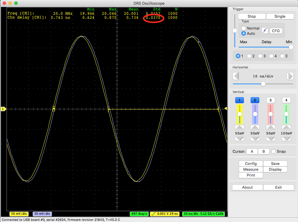
If I increase the frequency to 100 MHz and increase the amplitude, I get a better resolution:
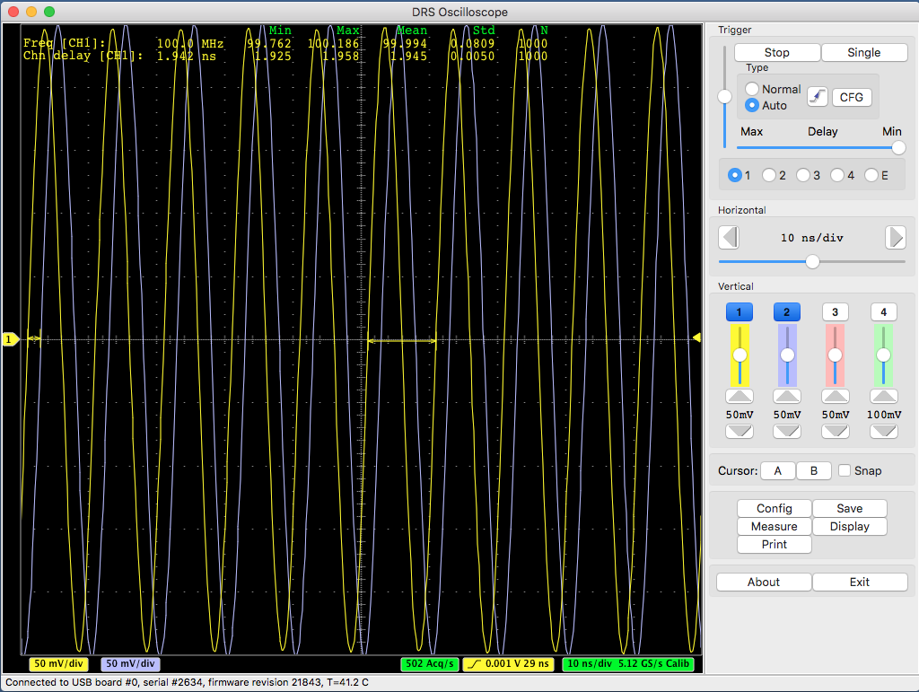
This is 5 ps which is better than 37 ps, but still not 2.5 ps. This can only be reached by sending single pulses to the evaluation board which have a rise time of > 300 mV / ns, which can be seen here:
It is important to understand the relation timing - resolution vs. rise time / noise as explained in the quoted paper. If you have tiny pulses from your detector, you never will be able to measure excellent timing. This is physics, and not related to the specific electronics you are using.
Best regards,
Stefan
|
|
|
545
|
Mon Oct 10 12:03:27 2016 |
Stefan Ritt | time difference between 2 channels only ~30-35ps @ 5GSmples/s | Ok, I got it. The timing resolution is affected by the signal-to-noise ratio over the rise-time of your signal. You find the full formula herer:
https://arxiv.org/abs/1405.4975
Your sine wave input signal has a slow rise time, and therefore limits the time resolution. I reproduced your measurement with a 20 MHz sine wave and got the same result:
If I increase the frequency to 100 MHz and increase the amplitude, I get a better resolution:
This is 5 ps which is better than 37 ps, but still not 2.5 ps. This can only be reached by sending single pulses to the evaluation board which have a rise time of > 300 mV / ns, which can be seen here:
It is important to understand the relation timing - resolution vs. rise time / noise as explained in the quoted paper. If you have tiny pulses from your detector, you never will be able to measure excellent timing. This is physics, and not related to the specific electronics you are using.
Best regards,
Stefan
|
|
544
|
Mon Oct 10 11:30:37 2016 |
Danny Petschke | time difference between 2 channels only ~30-35ps @ 5GSmples/s | Hello Stefan,
Chn2 & Chn3 were used for delay-determination as you can see on the second picture.
The second picture shows all 4 Channels without any voltage input.
On Channel 4 streaks (red circle) occur often and Channel 1 has totally different Offset (Picture 1).
Thanks
| Stefan Ritt wrote: |
|
Can you post a screenshot of your measurement?
Stefan
| Danny Petschke wrote: |
|
(Board Type:9, DRS4)
Hello,
I´m trying to reach the timig resolution of about 2.5ps as written in the manual.
My settings are:
5GSamples/s
+/-0.5V
I followed the instructions of the manual. The chip was warm and ran about 10h. Then, Timing- followed by Voltage-Calibration.
The test-signal is a splittet sine-wave of 20MHz (function-generator) brought on A0 and A1 (A1 signal is delayed by 1ns-cable).
I´ve been testing different trigger-logic: (Chn1 AND Chn2), (Chn1 OR Chn2) and only Chn1 or Chn2.
Trigger-levels were changed too.
All setups show the same result of 1.009ns +/- 30-35ns (results from the DRS-Oscilloscope).
What is wrong from my side?
Thanks a lot for your help
|
|
|
| Attachment 1: allChannels_zero_scaled.png
|

|
| Attachment 2: Chn2_Chn3_1ns_delay_scaled.png
|

|
|
543
|
Sun Oct 9 11:39:18 2016 |
Stefan Ritt | time difference between 2 channels only ~30-35ps @ 5GSmples/s | Can you post a screenshot of your measurement?
Stefan
| Danny Petschke wrote: |
|
(Board Type:9, DRS4)
Hello,
I´m trying to reach the timig resolution of about 2.5ps as written in the manual.
My settings are:
5GSamples/s
+/-0.5V
I followed the instructions of the manual. The chip was warm and ran about 10h. Then, Timing- followed by Voltage-Calibration.
The test-signal is a splittet sine-wave of 20MHz (function-generator) brought on A0 and A1 (A1 signal is delayed by 1ns-cable).
I´ve been testing different trigger-logic: (Chn1 AND Chn2), (Chn1 OR Chn2) and only Chn1 or Chn2.
Trigger-levels were changed too.
All setups show the same result of 1.009ns +/- 30-35ns (results from the DRS-Oscilloscope).
What is wrong from my side?
Thanks a lot for your help
|
|
|
542
|
Sun Oct 9 10:43:35 2016 |
Danny Petschke | time difference between 2 channels only ~30-35ps @ 5GSmples/s | (Board Type:9, DRS4)
Hello,
I´m trying to reach the timig resolution of about 2.5ps as written in the manual.
My settings are:
5GSamples/s
+/-0.5V
I followed the instructions of the manual. The chip was warm and ran about 10h. Then, Timing- followed by Voltage-Calibration.
The test-signal is a splittet sine-wave of 20MHz (function-generator) brought on A0 and A1 (A1 signal is delayed by 1ns-cable).
I´ve been testing different trigger-logic: (Chn1 AND Chn2), (Chn1 OR Chn2) and only Chn1 or Chn2.
Trigger-levels were changed too.
All setups show the same result of 1.009ns +/- 30-35ns (results from the DRS-Oscilloscope).
What is wrong from my side?
Thanks a lot for your help |
|
541
|
Thu Oct 6 15:23:18 2016 |
Will Flanagan | | Hi Stefan,
That is exactly what I'm looking for. Thanks again!
Will |
|
540
|
Thu Oct 6 11:18:05 2016 |
Stefan Ritt | Timestamp for each DRS4 waveform | In the mentioned read_binary.cpp file you have the line where you read the event header
i = fread(&eh, sizeof(eh), 1, f);
The C structure eh now contains the full timestamp, and you can access it with
eh.year

eh.month

eh.day

eh.hour

eh.minute

eh.second

eh.millisecond
Cheers,
Stefan
| Will Flanagan wrote: |
|
Hi DRS4 Experts,
I have been analyzing DRS4 binary data with scripts based on Stefan's (very helpful!) macro:
https://midas.psi.ch/elogs/DRS4+Forum/361
I would now like to look at the stability of my waveforms over a long period of time. In order to do this, I would need a timestamp encoded with each waveform. Are there timestamps within default DRS4 binary data? If so, does anyone have sample code for extracting them?
Best Regards,
Will
|
|
|
539
|
Wed Oct 5 22:43:29 2016 |
Will Flanagan | Timestamp for each DRS4 waveform | Hi DRS4 Experts,
I have been analyzing DRS4 binary data with scripts based on Stefan's (very helpful!) macro:
https://midas.psi.ch/elogs/DRS4+Forum/361
I would now like to look at the stability of my waveforms over a long period of time. In order to do this, I would need a timestamp encoded with each waveform. Are there timestamps within default DRS4 binary data? If so, does anyone have sample code for extracting them?
Best Regards,
Will |
|
538
|
Fri Sep 30 17:03:38 2016 |
Stefan Ritt | Output Timing Drifting | Hi Jacob,
you are missing the timing calibration. Each sampling cell has not the same width. Running at 5 GSPS, cell widths scatter from 150 ps to 250 ps. If you integrate these widhts, you get a time scale which can be off by a few ns between chips, something you see in your plot. Here is a paper which explains in detail how to do a timing calibration: https://arxiv.org/abs/1405.4975
Cheers,
Stefan
| Jacob Hwang wrote: |
|
Hello,
I have designed four DRS4 chips (36 channels) on my board running at 1GHz (REFCLK=488.28KHz) and ROI mode. All 4 chips' REFCLK, DWRITE, RSRLOAD, and SRCLK are buffer driven by the same source. SRCLK is set to 40MHz to reduce the readout time.
If I injected a sine waveform, buffered and splitted into all 36 channels,I noticed all 9 channels on each DRS4 chip output almost the same as expected. But the output phase from chip to chip is drifting as shown in attached picture which is from two different channels of different chips. From the few boards I have built, I found few chips are drifting more than the others and is different on every board.
The sympton look like the DRS4 internal PLL is drifting, but I checked the DTAP output on every chip and found it's dead-lock steady even I used persistance setting on my oscilloscope. Do you have any suggestion how to attack this problem? Thank you.
Jacob Hwang
|
|
|
537
|
Thu Sep 29 17:26:13 2016 |
Jacob Hwang | Output Timing Drifting | Hello,
I have designed four DRS4 chips (36 channels) on my board running at 1GHz (REFCLK=488.28KHz) and ROI mode. All 4 chips' REFCLK, DWRITE, RSRLOAD, and SRCLK are buffer driven by the same source. SRCLK is set to 40MHz to reduce the readout time.
If I injected a sine waveform, buffered and splitted into all 36 channels,I noticed all 9 channels on each DRS4 chip output almost the same as expected. But the output phase from chip to chip is drifting as shown in attached picture which is from two different channels of different chips. From the few boards I have built, I found few chips are drifting more than the others and is different on every board.
The sympton look like the DRS4 internal PLL is drifting, but I checked the DTAP output on every chip and found it's dead-lock steady even I used persistance setting on my oscilloscope. Do you have any suggestion how to attack this problem? Thank you.
Jacob Hwang
|
| Attachment 1: Output_Drifting.jpg
|

|
|
536
|
Mon Aug 29 12:51:48 2016 |
Stefan Ritt | increment write config register on the fly? | The problem is when you change the write config register from 11111111 to 01111111, or from 00001111 to 00000111, then the last 256 sampels of the previous channel (in the first case #0, in the scond #4) would be overwritten as soon as dwrite =1 again. So you loose 1/4 ef each channel.
Concerning the readout, indeed you can keep track in the FPGA, but only with a certainty of a few cells. This gives some timing inacccuracy of maybe 10-20 ns, which certainly would be disturbing you.
| benjamin legeyt wrote: |
|
If I may trouble you for a little more information, the critical point then is that there should not be any zeroes in the write config register while the sampling is active? In case it was unclear I would only be reading out once sampling was stopped (dwrite = 0).
As for the readout, I know that I would have to read out all 1024 samples each time, and keep track of where each channel stopped in the FPGA. I would never know the exact cell where sampling stopped but I hoped that if I discard some number of cells on each side of the expected stopping point that I would be OK.
Thanks again
| Stefan Ritt wrote: |
|
The issue with "stopping at cell 767" would also affect this mode of operation. Furthermore, the DRS4 chip has only 10 bit register which records in which cell the event has occured, and where the readout must be started. If you record 8 separate events, you don't know where to start the readout.
The DRS5 chip will have all this possibilitied, but unfortunately it won't be ready before 2-3 years from now.
Stefan
| benjamin legeyt wrote: |
|
Hello,
I have a question about using the write config register to enable/disable sampling on the fly. I am looking to instrument an experiment at EPFL where multiple short events need to be captured during a 20us period followed by an 80us quiet period during which we could read out the chip. Would it be possible to start an acquisition with all channels seeing the same signal and the write config register set to 111111111 and then shift a zero into the write config reg after each event is detected to freeze the channels in time one-by-one? In this way we could measure up to 8 different events during the active period and then read them all out together during the quiet period. I have read the posts about the simultaneous read-write mode and the issue with waveforms stopping at cell 767. not knowing the exact details of what causes this issue I wonder if it would effect this sort of operation? Also, I would like to know if dwrite must be de-asserted while the write config register is being updated or if it could be done while the sampling is active? The latter would obviously be preferable as we would not incur any dead-time during the active period.
Thanks in advance for the information,
Benjamin LeGeyt
|
|
|
|
|
535
|
Mon Aug 29 12:18:49 2016 |
benjamin legeyt | increment write config register on the fly? | If I may trouble you for a little more information, the critical point then is that there should not be any zeroes in the write config register while the sampling is active? In case it was unclear I would only be reading out once sampling was stopped (dwrite = 0).
As for the readout, I know that I would have to read out all 1024 samples each time, and keep track of where each channel stopped in the FPGA. I would never know the exact cell where sampling stopped but I hoped that if I discard some number of cells on each side of the expected stopping point that I would be OK.
Thanks again
| Stefan Ritt wrote: |
|
The issue with "stopping at cell 767" would also affect this mode of operation. Furthermore, the DRS4 chip has only 10 bit register which records in which cell the event has occured, and where the readout must be started. If you record 8 separate events, you don't know where to start the readout.
The DRS5 chip will have all this possibilitied, but unfortunately it won't be ready before 2-3 years from now.
Stefan
| benjamin legeyt wrote: |
|
Hello,
I have a question about using the write config register to enable/disable sampling on the fly. I am looking to instrument an experiment at EPFL where multiple short events need to be captured during a 20us period followed by an 80us quiet period during which we could read out the chip. Would it be possible to start an acquisition with all channels seeing the same signal and the write config register set to 111111111 and then shift a zero into the write config reg after each event is detected to freeze the channels in time one-by-one? In this way we could measure up to 8 different events during the active period and then read them all out together during the quiet period. I have read the posts about the simultaneous read-write mode and the issue with waveforms stopping at cell 767. not knowing the exact details of what causes this issue I wonder if it would effect this sort of operation? Also, I would like to know if dwrite must be de-asserted while the write config register is being updated or if it could be done while the sampling is active? The latter would obviously be preferable as we would not incur any dead-time during the active period.
Thanks in advance for the information,
Benjamin LeGeyt
|
|
|
|
534
|
Mon Aug 29 10:57:33 2016 |
Stefan Ritt | increment write config register on the fly? | The issue with "stopping at cell 767" would also affect this mode of operation. Furthermore, the DRS4 chip has only 10 bit register which records in which cell the event has occured, and where the readout must be started. If you record 8 separate events, you don't know where to start the readout.
The DRS5 chip will have all this possibilitied, but unfortunately it won't be ready before 2-3 years from now.
Stefan
| benjamin legeyt wrote: |
|
Hello,
I have a question about using the write config register to enable/disable sampling on the fly. I am looking to instrument an experiment at EPFL where multiple short events need to be captured during a 20us period followed by an 80us quiet period during which we could read out the chip. Would it be possible to start an acquisition with all channels seeing the same signal and the write config register set to 111111111 and then shift a zero into the write config reg after each event is detected to freeze the channels in time one-by-one? In this way we could measure up to 8 different events during the active period and then read them all out together during the quiet period. I have read the posts about the simultaneous read-write mode and the issue with waveforms stopping at cell 767. not knowing the exact details of what causes this issue I wonder if it would effect this sort of operation? Also, I would like to know if dwrite must be de-asserted while the write config register is being updated or if it could be done while the sampling is active? The latter would obviously be preferable as we would not incur any dead-time during the active period.
Thanks in advance for the information,
Benjamin LeGeyt
|
|
|
533
|
Mon Aug 29 09:36:34 2016 |
benjamin legeyt | increment write config register on the fly? | Hello,
I have a question about using the write config register to enable/disable sampling on the fly. I am looking to instrument an experiment at EPFL where multiple short events need to be captured during a 20us period followed by an 80us quiet period during which we could read out the chip. Would it be possible to start an acquisition with all channels seeing the same signal and the write config register set to 111111111 and then shift a zero into the write config reg after each event is detected to freeze the channels in time one-by-one? In this way we could measure up to 8 different events during the active period and then read them all out together during the quiet period. I have read the posts about the simultaneous read-write mode and the issue with waveforms stopping at cell 767. not knowing the exact details of what causes this issue I wonder if it would effect this sort of operation? Also, I would like to know if dwrite must be de-asserted while the write config register is being updated or if it could be done while the sampling is active? The latter would obviously be preferable as we would not incur any dead-time during the active period.
Thanks in advance for the information,
Benjamin LeGeyt |
|
531
|
Wed Jun 29 09:10:01 2016 |
Stefan Ritt | Negative input signals | Hello everybody,
I get often asked if the DRS4 evaluation board can accomodate negative input pulses going to -1V. This is unfortunately not possible, since the board is mainly for evaluation of the DRS4 chip and should not be seen as a complete oscilloscope with flexible input stage. So the maximum it can do is -0.5V to +0.5V or 0V to 1V. For -1V signals, one can use however a passive inverter like this one:
http://www.phillipsscientific.com/pdf/460ds.pdf
And for signals going furhter (-2V, -10V) one can use a passive attenuator like this one:
http://www.pomonaelectronics.com/pdf/d4108_K5513_101.pdf
Best regards,
Stefan
|
|
530
|
Wed Jun 15 14:49:00 2016 |
Stefan Ritt | problems of DRS4 | 1. Simultaneous writing and reading is not possible with the DRS4 chip. The manual says differently on p. 14, but due to a bug in the chip waveforms get clipped at the end if one does that. We hopt to fix this problem in a future version of the chip.
2. You can cascade 2,4 or 8 channels. If you cascade 8 channels and run at 1 GSPS, you digitize a window of 8 us. If you have 16 signals, you then need 16 chips.
/Stefan
| Michael wrote: |
|
Hi
I want to use DRS4 to digitize 16 channels of signals. The width of signal is about 20 ns, with frequency of 50Hz. The time differences between these 16 signals are not constant, arranging from 3us to 0. I am confused about this in some aspects.
- Can I use SIMULTANEOUS WRITINT AND READING to realize this? I saw the VHDL program, and if I understand it correctly, it did not work at this state.
- Or sampling at 1GSPS, using CASCADING OF CHANNELS, I can sample signal at most 4us or 8us, then digitizing all signals of one chip. Have you tested 4 or more channels cascading before?
Besides, any advice will be helpful!
Thank you.
|
|
|
Draft
|
Sun Jun 12 08:49:54 2016 |
Michael | problems of DRS4 | Hi
I want to use DRS4 to digitize 16 channels of signals. The width of signal is about 20 ns, with frequency of 50Hz. The time differences between these 16 signals are not constant, arranging from 3us to 0. I am confused about this in some aspects.
- Can I use SIMULTANEOUS WRITINT AND READING to realize this? I saw the VHDL program, and if I understand it correctly, it did not work at this state.
- Or sampling at 1GSPS, using CASCADING OF CHANNELS, I can sample signal at most 4us or 8us, then digitizing all signals of one chip. Have you tested 4 or more channels cascading before?
Besides, any advice will be helpful!
Thank you. |
|
528
|
Sun Jun 12 08:45:52 2016 |
Michael | problems of DRS4 | Hi
I want to use DRS4 to digitize 16 channels of signals. The width of signal is about 20 ns, with frequency of 50Hz. The time differences between these 16 signals are not constant, arranging from 3us to 0. I am confused about this in some aspects.
- Can I use SIMULTANEOUS WRITINT AND READING to realize this? I saw the VHDL program, and if I understand it correctly, it did not work at this state.
- Or sampling at 1GSPS, using CASCADING OF CHANNELS, I can sample signal at most 4us or 8us, then digitizing all signals of one chip. Have you tested 4 or more channels cascading before?
Besides, any advice will be helpful!
Thank you. |
|
527
|
Wed Jun 1 23:16:01 2016 |
Stefan Ritt | problems when stop cell >= 767 ?? | I cannot confirm the story with the "stop capacitor > 767". It can be seen from your plots that the distribution of stop cells are even, no holes or bins with double height.
There is an issue with cell 767, but this is when one tries to do simultaneous reading/writing to the chip. This does not really work as writen in the data sheet. Waveforms sometimgs get cut off at cell 767. But the stop cell is always correct, otherwise one could not calibrate the data. If you use the evaluation board for example, which is perfectly calibrated, and introduce an "artifical" shift like
if stop cell > 767 then
stop cell = stop cell + 1
then you would see that the voltage calibration would become wrong and very noisy.
Stefan
| Dominik Neise wrote: |
|
Hello Stefan,
some colleages told me a story, I was neither able to confirm nor find anything in the datsheet about. According to them:
For some internal reason of the DRS4, if the “stop capacitor” of the DRS4 is >= 767, the true stop channel is one before the stop channel read from the DRS4. In other words, the stop channel which returns the DRS4 shifts after sampling to the capacitor ID 766.
Can you confirm that, or even say a few words about that matter?
I wanted to confirm this by plotting the stop cell distribution for random triggered data, taken with one of the FACT boards. I assumed (possibly misunderstanding the matter), that this would lead to missing values in the area of stop cell 767, but cannot see any significant excess or lack of entries in that area.
|
|
|
526
|
Wed Jun 1 22:29:01 2016 |
Dominik Neise | problems when stop cell >= 767 ?? | Hello Stefan,
some colleages told me a story, I was neither able to confirm nor find anything in the datsheet about. According to them:
For some internal reason of the DRS4, if the “stop capacitor” of the DRS4 is >= 767, the true stop channel is one before the stop channel read from the DRS4. In other words, the stop channel which returns the DRS4 shifts after sampling to the capacitor ID 766.
Can you confirm that, or even say a few words about that matter?
I wanted to confirm this by plotting the stop cell distribution for random triggered data, taken with one of the FACT boards. I assumed (possibly misunderstanding the matter), that this would lead to missing values in the area of stop cell 767, but cannot see any significant excess or lack of entries in that area.
|
| Attachment 1: stop_cell_distribution.png
|

|
|
525
|
Thu May 12 12:38:17 2016 |
Stefan Ritt | DRS4 Macro to save events | Dear Maksat,
If your car does not run, and you call the car dealer and tell him "my car does not run", what will the car dealer ask you? Eh... ? Right ! He will ask "what are the symptoms, what did you try, what did and what did not work". Here it's the same. "was not able to get it work" is not a valid statement, since I have absolutely no idea what did not work and what you did try.
The official way is to follow the instruction in the evlauation board manual on section 2.4 - Installation under Linux. If that does not work, please be a bit more precise what errors you get.
Cheers,
Stefan
| Maksat wrote: |
|
Dear Stefan,
I am trying to setup DRS inside radiation enclosure and would like to write a simple script that will automatically save certain number of events.
Could you please point to me an example that can I use for Mac OS? I saw there is drs_exam.cpp in the directory but was not able to get work in Mac OS. Any help would be greatly appreciated.
Thanks
|
|
|
524
|
Thu May 12 08:16:41 2016 |
Stefan Ritt | Problem For Software Download | Can you tell me (screendump) what is the problem on the web site https://www.psi.ch/drs/software-download ? It should redirect you to
https://www.dropbox.com/sh/qul1cgtm4x7zx13/AADKQ-qGQGdAHPu6OR3vTNY0a?dl=0
for the Windows download.
I cannot send executables via email, that won't go though any spam filter.
Stefan
| Yu wrote: |
|
Hi
I can't download the software for windows on this website 'www.psi.ch/drs/software-download', there is some mistake when i click on download.
If convenient, can you send the software Version 5.0.5 for windows to me? My E-mail address is 'yuhaiyang421@163.com'. Thank you!
Best Regards
Yu
|
|
|
523
|
Thu May 12 05:18:47 2016 |
Yu | Problem For Software Download | Hi
I can't download the software for windows on this website 'www.psi.ch/drs/software-download', there is some mistake when i click on download.
If convenient, can you send the software Version 5.0.5 for windows to me? My E-mail address is 'yuhaiyang421@163.com'. Thank you!
Best Regards
Yu |
|
522
|
Wed May 11 15:48:57 2016 |
SANDJONG Saturnin Orly | Probl�me de Calibration de la DRS4 | Bonjour, Je suis en stage dans un laboratoire ou on utilise pour echantillonnage des données, une cartes DRS4 5GSPS avec 1024 cell, mon probléme réside dans la partie Calibration en tension selon l'article "Novel Calibration Method for Switched Capacitor Arrays Enables Time Measurements with Sub-Picosecond Resolution".
En fait je ne comprends pas précisément ces 3 parties de la calibration en tension. Quelqu'un pourras t-il s'il vous plait m'expliquer assez clairement avec des exemples comment il faut s'y prendre?
Merci et bien Cordialement. |
| Attachment 1: piedestaux_per_time.jpg
|

|
|
521
|
Wed May 11 04:01:14 2016 |
Maksat | DRS4 Macro to save events | Dear Stefan,
I am trying to setup DRS inside radiation enclosure and would like to write a simple script that will automatically save certain number of events.
Could you please point to me an example that can I use for Mac OS? I saw there is drs_exam.cpp in the directory but was not able to get work in Mac OS. Any help would be greatly appreciated.
Thanks
|
|
520
|
Mon May 2 14:31:28 2016 |
Dmitry Hits | two DRS4 boards configuration with 2048 samples each | Hi Stefan
Any chance you have time to fix the software for multiboard configuration with 2048 samples each. I tried 5.0.5, but drsosc still shows only half of the waveform.
Dmitry
| Stefan Ritt wrote: |
|
The multi-board mode has never been tested with 2048 samples, so is very likely not to work. I don't know yet how much work this will be to fix, but I'm on a business trip the next three weeks and probably will only have time to look at it when I return.
Stefan
| Dmitry Hits wrote: |
|
Dear Stefan,
I daisy-chained two boards (master sn#: 2514 - slave sn#: 2513) each with 2048 samples. However, when I use drsosc and put check mark in "configure multi-board daisy-chain" I see only 1024 samples. Namely, the first 1024 samples, the last part is missing. When I remove this check mark, I see all 2048 samples. Is there a simple software fix for this or is it a more involved firmware limitation?
Other parameters: software version: 5.0.4, firmware version 21305, configured for 0.7 GSPS, display at 500 ns/div
Thank you,
Dmitry Hits.
|
|
|
|
519
|
Thu Apr 28 15:47:53 2016 |
Stefan Ritt | New software version and binary format | A new software version 5.0.5 has been released today. This fixes a few bugs in multi-board configurations, and adds saving of the scaler values into XML and binary files. Please note that the binary file format has been changed for that. The new format is described in an updated manual (page 25), and reflected in a new read_binary.cpp program contained in the distribution.
/Stefan |
|
518
|
Thu Apr 28 15:46:34 2016 |
Stefan Ritt | Best settings for time measurements | The DRS4 chip has been designed to work best at high sampling speeds. At 700 MSPS, the chip is at it's limit and timing is very poorr (ns?). In order to get good timing, run it at least at 2 GSPS.
Stefan
| Abaz Kryemadhi wrote: |
|
I am studing some pulses that are about 200-300 ns wide and a rise time of few ns, which settings would be best for coincidence time measurements?
In some preliminary work I found for 700 MegaS the time measurement is better without time calibration (in -0.05 to 1V) rather than with time calibration in -0.5 to 0.5, my pulses are about 60 mV. Is it expected that always with time calibration time accuracy would be better or depends?
Also I use this code snippet to find time for channel 1 and the same idea for chan. 2.
// find peak in channel 1 above threshold
for (i=0 ; i<1022 ; i++)
if (waveform[0][i] < threshold1 && waveform[0][i+1] >= threshold1) {
tt1 = (threshold1-waveform[0][i])/(waveform[0][i+1]-waveform[0][i])*(time[0][i+1]-time[0][i])+time[0][i];
break;
}
Thanks!
Abaz
|
|
|
517
|
Wed Apr 27 20:04:12 2016 |
Abaz Kryemadhi | Best settings for time measurements | I am studing some pulses that are about 200-300 ns wide and a rise time of few ns, which settings would be best for coincidence time measurements?
In some preliminary work I found for 700 MegaS the time measurement is better without time calibration (in -0.05 to 1V) rather than with time calibration in -0.5 to 0.5, my pulses are about 60 mV. Is it expected that always with time calibration time accuracy would be better or depends?
Also I use this code snippet to find time for channel 1 and the same idea for chan. 2.
// find peak in channel 1 above threshold
for (i=0 ; i<1022 ; i++)
if (waveform[0][i] < threshold1 && waveform[0][i+1] >= threshold1) {
tt1 = (threshold1-waveform[0][i])/(waveform[0][i+1]-waveform[0][i])*(time[0][i+1]-time[0][i])+time[0][i];
break;
}
Thanks!
Abaz |
|
516
|
Wed Apr 27 09:51:37 2016 |
Toshihiro Nonaka | serial number problem | The serial number has been fixed by using drscl. Thank you!
| Stefan Ritt wrote: |
|
If dis- and reconnecting the board does not help, there is the (small) chance that the serial number got erased in the board. You can re-set it with the "drscl" command line tool:
$ drscl
Found DRS4 board 0 on USB, serial #0, firmware revision 21305
B0> serial 2172
| Toshihiro Nonaka wrote: |
|
Dear all,
I'm using 3 DRS boards simultaneously and their serial numbers are 2169, 2170, 2172 respectively.
Recently however, I obtain serial number "0" by DRSBoard::GetBoardSerialNumber() for #2172 board.
Data taking can be done without any problems, but I'd like to know what is happening.
Any advice?
Thank you.
Toshihiro Nonaka
|
|
|
|
515
|
Wed Apr 27 09:04:01 2016 |
Stefan Ritt | serial number problem | If dis- and reconnecting the board does not help, there is the (small) chance that the serial number got erased in the board. You can re-set it with the "drscl" command line tool:
$ drscl
Found DRS4 board 0 on USB, serial #0, firmware revision 21305
B0> serial 2172
| Toshihiro Nonaka wrote: |
|
Dear all,
I'm using 3 DRS boards simultaneously and their serial numbers are 2169, 2170, 2172 respectively.
Recently however, I obtain serial number "0" by DRSBoard::GetBoardSerialNumber() for #2172 board.
Data taking can be done without any problems, but I'd like to know what is happening.
Any advice?
Thank you.
Toshihiro Nonaka
|
|
|
514
|
Wed Apr 27 08:14:14 2016 |
Toshihiro Nonaka | serial number problem | Dear all,
I'm using 3 DRS boards simultaneously and their serial numbers are 2169, 2170, 2172 respectively.
Recently however, I obtain serial number "0" by DRSBoard::GetBoardSerialNumber() for #2172 board.
Data taking can be done without any problems, but I'd like to know what is happening.
Any advice?
Thank you.
Toshihiro Nonaka |
| Attachment 1: serial.png
|

|
|
513
|
Tue Apr 26 13:42:42 2016 |
Stefan Ritt | DRS4 purchase information | Just be patient. Anita is not at work this week.
| Konstantin Gusev wrote: |
|
Hi,
I can't contact with Anita Van Loon about DSR4 chip's price and delivery.
Did you still sell it? Can you provide me this information?
|
|
|
512
|
Tue Apr 26 09:54:16 2016 |
Stefan Ritt | Negative fCellDT values from GetTimeCalibration() | I just realized that the negative bin widht is not explicitly mentioned in the quoted paper. So let me explain it here:
The negative value of cell 498 is correct and "real" in the sense that the signal is first captured in cell 498 and later in cell 497. This is due to the exact layout of the cells on the chip and the input signal. Cell 498 is simply much closer to the input, so sees the signal earlier than cell 497, even if it's triggerd after cell 497. So nothing to worry about.
Stefan
| Daniel Stricker-Shaver wrote: |
|
Hi Kyle,
If I remember right the negative sampling width happens only for 498 and at high sampling speeds. It is described in a paper from Stefan:
http://arxiv.org/pdf/1405.4975.pdf
or
“Novel Calibration Method for Switched Capacitor Arrays Enables Time Measurements With Sub-Picosecond Resolution”( IEEE Transactions on Nuclear Science 61 (2014),Nr. 6, 3607–3617)
| Kyle Weinfurther wrote: |
|
Hello Stefan,
I am using four DRS4 v5 eval boards to digitize 16 channels of data. I have recently changed from saving the timing information of the waveform using GetTime() to GetTimeCalibration(). When changing over, I noticed that some values for fCellDT for cell 498 are negative. Over the 16 channels used, 4 of them have negative time bin widths for cell 498 while the other 12 channels are very close to 0 (in the ~10 ps range). One of the eval boards has no negative fCellDT whereas the other three boards have one or two channels with negative values.
Upon further inspection, I checked the time between samples of GetTime() and found the same results in cell 498. After finding this, I did a timing calibration again with CalibrateTiming() even though in a different post on the discussion forum you said it was valid for a wide range of temperatures and a long time (years). This still allowed the negative fCellDT values to persist.
Is this a common occurance? If so, is there a method to fix this issue? Is there a reason for cell 498 to have a small value for fCellDT? I searched the discussion forum and did not find anything relating to this issue.
Attached are a couple waveform traces using GetTime() zoomed in on cell 498.
Thanks,
Kyle Weinfurther
|
|
|
|
511
|
Sat Apr 23 12:33:17 2016 |
Daniel Stricker-Shaver | Negative fCellDT values from GetTimeCalibration() | Hi Kyle,
If I remember right the negative sampling width happens only for 498 and at high sampling speeds. It is described in a paper from Stefan:
http://arxiv.org/pdf/1405.4975.pdf
or
“Novel Calibration Method for Switched Capacitor Arrays Enables Time Measurements With Sub-Picosecond Resolution”( IEEE Transactions on Nuclear Science 61 (2014),Nr. 6, 3607–3617)
| Kyle Weinfurther wrote: |
|
Hello Stefan,
I am using four DRS4 v5 eval boards to digitize 16 channels of data. I have recently changed from saving the timing information of the waveform using GetTime() to GetTimeCalibration(). When changing over, I noticed that some values for fCellDT for cell 498 are negative. Over the 16 channels used, 4 of them have negative time bin widths for cell 498 while the other 12 channels are very close to 0 (in the ~10 ps range). One of the eval boards has no negative fCellDT whereas the other three boards have one or two channels with negative values.
Upon further inspection, I checked the time between samples of GetTime() and found the same results in cell 498. After finding this, I did a timing calibration again with CalibrateTiming() even though in a different post on the discussion forum you said it was valid for a wide range of temperatures and a long time (years). This still allowed the negative fCellDT values to persist.
Is this a common occurance? If so, is there a method to fix this issue? Is there a reason for cell 498 to have a small value for fCellDT? I searched the discussion forum and did not find anything relating to this issue.
Attached are a couple waveform traces using GetTime() zoomed in on cell 498.
Thanks,
Kyle Weinfurther
|
|
|
509
|
Thu Apr 21 22:16:43 2016 |
Kyle Weinfurther | Negative fCellDT values from GetTimeCalibration() | Hello Stefan,
I am using four DRS4 v5 eval boards to digitize 16 channels of data. I have recently changed from saving the timing information of the waveform using GetTime() to GetTimeCalibration(). When changing over, I noticed that some values for fCellDT for cell 498 are negative. Over the 16 channels used, 4 of them have negative time bin widths for cell 498 while the other 12 channels are very close to 0 (in the ~10 ps range). One of the eval boards has no negative fCellDT whereas the other three boards have one or two channels with negative values.
Upon further inspection, I checked the time between samples of GetTime() and found the same results in cell 498. After finding this, I did a timing calibration again with CalibrateTiming() even though in a different post on the discussion forum you said it was valid for a wide range of temperatures and a long time (years). This still allowed the negative fCellDT values to persist.
Is this a common occurance? If so, is there a method to fix this issue? Is there a reason for cell 498 to have a small value for fCellDT? I searched the discussion forum and did not find anything relating to this issue.
Attached are a couple waveform traces using GetTime() zoomed in on cell 498.
Thanks,
Kyle Weinfurther |
| Attachment 1: ch5.png
|

|
| Attachment 2: ch7.png
|

|
| Attachment 3: ch9.png
|

|
|
508
|
Fri Apr 15 12:58:46 2016 |
Konstantin Gusev | DRS4 purchase information | Hi,
I can't contact with Anita Van Loon about DSR4 chip's price and delivery.
Did you still sell it? Can you provide me this information? |
|
507
|
Wed Apr 6 09:46:10 2016 |
Daniel Dribin | DRS Oscilloscope freezing after a long run |
| Martin Petriska wrote: |
|
| Stefan Ritt wrote: |
|
I tried this night to run the board at a 10 Hz rate with an external pulser, without writing, and it did not freeze after ~14 hours of running on Mac OSX. This night I will try again with writing.
Stefan
| Stefan Ritt wrote: |
|
Then it seems that there is some USB communication problem. I heard this also from other people, that the USB data transfer under Windows has sometimes problems. I develop and run the board under Mac OSX, and there the same software runs for days without problem. So I guess it's related to the underlying libusb lib which is used by the DRS oscilloscope, on which I have no influence. So the only advice I can give is to take shorter series of data. Anyhow the board is not considered a full DAQ system, just an "evaluation board" which means one can try the DRS4 chip and play with it. For serious business one should build own electronics with the chip. Anyhow we are currently developping an Ethernet board which allows much faster acquisition rates, so USB will be obsolete some day. Nevertheless I will try to reproduce your problem and see if I can do anything. At what trigger rate does it show up most prominently?
Stefan
| Daniel Dribin wrote: |
|
Dear Stefan Ritt,
Yes I use Windows 7, If the DRS Oscilloscope program stays on for a couple of hours without saving the data, the problem will occur. It seems it happens more often when there is data writing and when the rate of events is slow, about 100 events per second, at high rates it almost doesn't happen. Can it be temperature related?
Daniel
| Stefan Ritt wrote: |
|
Dear Daniel,
sorry my late reply, I'm pretty busy these days. The behavior you report has not been seen before, but I guess no one tried to take such long runs of data yet. Can you confirm that the problem also occurs without writing data to disk, or is it disk-related? I guess you use it under Windows 7, right?
Stefan
| Daniel Dribin wrote: |
|
Dear Stefan Ritt,
I am using a DRS4 v5 to do timing measurements of Positron lifetime. I use the DRS Oscilloscope with triggering on 2 channels when I have a coincidence. Attached is a picture with all the setting that I use. When I use the DRS4 for a long measurements of 5 million events for a couple of hours, the DRS Oscilloscope stops showing any signal .After the first restart of the program I get a strange signal which is at the bottom of the scope range of voltage picture below(in the picture I changed the vertical positions of the channels for better viewing). Only after a couple of DRS Oscilloscope restarts and USB reconnections do I get the results again.
I currently am using another DRS4 v5 and the same situation occurs again although with lower frequency.
What can I do to solve this problem?
thank you very much,
Daniel
|
|
|
|
|
Hi I have also positron annihilation system based on DRS4v4 cards. Its running several weeks, sometimes months, without freezing in windows7 64bit system (Pentium Core Quad 2Ghz, 4GRam). Problem was when widows was trying to install updates and restarted PC. In beginning I had some problem with memory leak in my application, but it was simple seen in task manager that application memory was rising and was need to find memory leak in application code. Now I remember card was sometimes freezing when room air conditioning with 2kW was starting and high electricity pulses were reason of USB problems, it helped to put air conditioner and PC in different power line input. Hope it help to solve zour problems.
Martin
|
I too have air conditioning in the room, not sure to which power line it is connected, but I'll try to check this aswell.
Thank you very much. |
|
506
|
Wed Apr 6 09:43:52 2016 |
Daniel Dribin | DRS Oscilloscope freezing after a long run | At hight rates I worked with files of up to 20 GB so I don't think this is the problem.
I will try to run it under Ubuntu and see if i can recreate the problem.
Thank you very much for the quick responses and help.
| Stefan Ritt wrote: |
|
Even with writing for one night no problem (see below). Have you checked how big your data file is? I guess there is a limit under Windows of 2 GB. If that's the case, you have to write shorter files.
|
|
|
505
|
Wed Apr 6 09:01:28 2016 |
Martin Petriska | DRS Oscilloscope freezing after a long run |
| Stefan Ritt wrote: |
|
I tried this night to run the board at a 10 Hz rate with an external pulser, without writing, and it did not freeze after ~14 hours of running on Mac OSX. This night I will try again with writing.
Stefan
| Stefan Ritt wrote: |
|
Then it seems that there is some USB communication problem. I heard this also from other people, that the USB data transfer under Windows has sometimes problems. I develop and run the board under Mac OSX, and there the same software runs for days without problem. So I guess it's related to the underlying libusb lib which is used by the DRS oscilloscope, on which I have no influence. So the only advice I can give is to take shorter series of data. Anyhow the board is not considered a full DAQ system, just an "evaluation board" which means one can try the DRS4 chip and play with it. For serious business one should build own electronics with the chip. Anyhow we are currently developping an Ethernet board which allows much faster acquisition rates, so USB will be obsolete some day. Nevertheless I will try to reproduce your problem and see if I can do anything. At what trigger rate does it show up most prominently?
Stefan
| Daniel Dribin wrote: |
|
Dear Stefan Ritt,
Yes I use Windows 7, If the DRS Oscilloscope program stays on for a couple of hours without saving the data, the problem will occur. It seems it happens more often when there is data writing and when the rate of events is slow, about 100 events per second, at high rates it almost doesn't happen. Can it be temperature related?
Daniel
| Stefan Ritt wrote: |
|
Dear Daniel,
sorry my late reply, I'm pretty busy these days. The behavior you report has not been seen before, but I guess no one tried to take such long runs of data yet. Can you confirm that the problem also occurs without writing data to disk, or is it disk-related? I guess you use it under Windows 7, right?
Stefan
| Daniel Dribin wrote: |
|
Dear Stefan Ritt,
I am using a DRS4 v5 to do timing measurements of Positron lifetime. I use the DRS Oscilloscope with triggering on 2 channels when I have a coincidence. Attached is a picture with all the setting that I use. When I use the DRS4 for a long measurements of 5 million events for a couple of hours, the DRS Oscilloscope stops showing any signal .After the first restart of the program I get a strange signal which is at the bottom of the scope range of voltage picture below(in the picture I changed the vertical positions of the channels for better viewing). Only after a couple of DRS Oscilloscope restarts and USB reconnections do I get the results again.
I currently am using another DRS4 v5 and the same situation occurs again although with lower frequency.
What can I do to solve this problem?
thank you very much,
Daniel
|
|
|
|
|
Hi I have also positron annihilation system based on DRS4v4 cards. Its running several weeks, sometimes months, without freezing in windows7 64bit system (Pentium Core Quad 2Ghz, 4GRam). Problem was when widows was trying to install updates and restarted PC. In beginning I had some problem with memory leak in my application, but it was simple seen in task manager that application memory was rising and was need to find memory leak in application code. Now I remember card was sometimes freezing when room air conditioning with 2kW was starting and high electricity pulses were reason of USB problems, it helped to put air conditioner and PC in different power line input. Hope it help to solve zour problems.
Martin |
|
504
|
Wed Apr 6 08:41:08 2016 |
Stefan Ritt | DRS Oscilloscope freezing after a long run | Even with writing for one night no problem (see below). Have you checked how big your data file is? I guess there is a limit under Windows of 2 GB. If that's the case, you have to write shorter files.
|
|
503
|
Tue Apr 5 16:08:59 2016 |
Stefan Ritt | DRS Oscilloscope freezing after a long run | I tried this night to run the board at a 10 Hz rate with an external pulser, without writing, and it did not freeze after ~14 hours of running on Mac OSX. This night I will try again with writing.
Stefan
| Stefan Ritt wrote: |
|
Then it seems that there is some USB communication problem. I heard this also from other people, that the USB data transfer under Windows has sometimes problems. I develop and run the board under Mac OSX, and there the same software runs for days without problem. So I guess it's related to the underlying libusb lib which is used by the DRS oscilloscope, on which I have no influence. So the only advice I can give is to take shorter series of data. Anyhow the board is not considered a full DAQ system, just an "evaluation board" which means one can try the DRS4 chip and play with it. For serious business one should build own electronics with the chip. Anyhow we are currently developping an Ethernet board which allows much faster acquisition rates, so USB will be obsolete some day. Nevertheless I will try to reproduce your problem and see if I can do anything. At what trigger rate does it show up most prominently?
Stefan
| Daniel Dribin wrote: |
|
Dear Stefan Ritt,
Yes I use Windows 7, If the DRS Oscilloscope program stays on for a couple of hours without saving the data, the problem will occur. It seems it happens more often when there is data writing and when the rate of events is slow, about 100 events per second, at high rates it almost doesn't happen. Can it be temperature related?
Daniel
| Stefan Ritt wrote: |
|
Dear Daniel,
sorry my late reply, I'm pretty busy these days. The behavior you report has not been seen before, but I guess no one tried to take such long runs of data yet. Can you confirm that the problem also occurs without writing data to disk, or is it disk-related? I guess you use it under Windows 7, right?
Stefan
| Daniel Dribin wrote: |
|
Dear Stefan Ritt,
I am using a DRS4 v5 to do timing measurements of Positron lifetime. I use the DRS Oscilloscope with triggering on 2 channels when I have a coincidence. Attached is a picture with all the setting that I use. When I use the DRS4 for a long measurements of 5 million events for a couple of hours, the DRS Oscilloscope stops showing any signal .After the first restart of the program I get a strange signal which is at the bottom of the scope range of voltage picture below(in the picture I changed the vertical positions of the channels for better viewing). Only after a couple of DRS Oscilloscope restarts and USB reconnections do I get the results again.
I currently am using another DRS4 v5 and the same situation occurs again although with lower frequency.
What can I do to solve this problem?
thank you very much,
Daniel
|
|
|
|
|
|
502
|
Mon Apr 4 12:08:15 2016 |
Stefan Ritt | DRS Oscilloscope freezing after a long run | Then it seems that there is some USB communication problem. I heard this also from other people, that the USB data transfer under Windows has sometimes problems. I develop and run the board under Mac OSX, and there the same software runs for days without problem. So I guess it's related to the underlying libusb lib which is used by the DRS oscilloscope, on which I have no influence. So the only advice I can give is to take shorter series of data. Anyhow the board is not considered a full DAQ system, just an "evaluation board" which means one can try the DRS4 chip and play with it. For serious business one should build own electronics with the chip. Anyhow we are currently developping an Ethernet board which allows much faster acquisition rates, so USB will be obsolete some day. Nevertheless I will try to reproduce your problem and see if I can do anything. At what trigger rate does it show up most prominently?
Stefan
| Daniel Dribin wrote: |
|
Dear Stefan Ritt,
Yes I use Windows 7, If the DRS Oscilloscope program stays on for a couple of hours without saving the data, the problem will occur. It seems it happens more often when there is data writing and when the rate of events is slow, about 100 events per second, at high rates it almost doesn't happen. Can it be temperature related?
Daniel
| Stefan Ritt wrote: |
|
Dear Daniel,
sorry my late reply, I'm pretty busy these days. The behavior you report has not been seen before, but I guess no one tried to take such long runs of data yet. Can you confirm that the problem also occurs without writing data to disk, or is it disk-related? I guess you use it under Windows 7, right?
Stefan
| Daniel Dribin wrote: |
|
Dear Stefan Ritt,
I am using a DRS4 v5 to do timing measurements of Positron lifetime. I use the DRS Oscilloscope with triggering on 2 channels when I have a coincidence. Attached is a picture with all the setting that I use. When I use the DRS4 for a long measurements of 5 million events for a couple of hours, the DRS Oscilloscope stops showing any signal .After the first restart of the program I get a strange signal which is at the bottom of the scope range of voltage picture below(in the picture I changed the vertical positions of the channels for better viewing). Only after a couple of DRS Oscilloscope restarts and USB reconnections do I get the results again.
I currently am using another DRS4 v5 and the same situation occurs again although with lower frequency.
What can I do to solve this problem?
thank you very much,
Daniel
|
|
|
|
|
501
|
Mon Apr 4 11:41:26 2016 |
Daniel Dribin | DRS Oscilloscope freezing after a long run | Dear Stefan Ritt,
Yes I use Windows 7, If the DRS Oscilloscope program stays on for a couple of hours without saving the data, the problem will occur. It seems it happens more often when there is data writing and when the rate of events is slow, about 100 events per second, at high rates it almost doesn't happen. Can it be temperature related?
Daniel
| Stefan Ritt wrote: |
|
Dear Daniel,
sorry my late reply, I'm pretty busy these days. The behavior you report has not been seen before, but I guess no one tried to take such long runs of data yet. Can you confirm that the problem also occurs without writing data to disk, or is it disk-related? I guess you use it under Windows 7, right?
Stefan
| Daniel Dribin wrote: |
|
Dear Stefan Ritt,
I am using a DRS4 v5 to do timing measurements of Positron lifetime. I use the DRS Oscilloscope with triggering on 2 channels when I have a coincidence. Attached is a picture with all the setting that I use. When I use the DRS4 for a long measurements of 5 million events for a couple of hours, the DRS Oscilloscope stops showing any signal .After the first restart of the program I get a strange signal which is at the bottom of the scope range of voltage picture below(in the picture I changed the vertical positions of the channels for better viewing). Only after a couple of DRS Oscilloscope restarts and USB reconnections do I get the results again.
I currently am using another DRS4 v5 and the same situation occurs again although with lower frequency.
What can I do to solve this problem?
thank you very much,
Daniel
|
|
|
|
500
|
Mon Apr 4 11:31:34 2016 |
Stefan Ritt | DRS Oscilloscope freezing after a long run | Dear Daniel,
sorry my late reply, I'm pretty busy these days. The behavior you report has not been seen before, but I guess no one tried to take such long runs of data yet. Can you confirm that the problem also occurs without writing data to disk, or is it disk-related? I guess you use it under Windows 7, right?
Stefan
| Daniel Dribin wrote: |
|
Dear Stefan Ritt,
I am using a DRS4 v5 to do timing measurements of Positron lifetime. I use the DRS Oscilloscope with triggering on 2 channels when I have a coincidence. Attached is a picture with all the setting that I use. When I use the DRS4 for a long measurements of 5 million events for a couple of hours, the DRS Oscilloscope stops showing any signal .After the first restart of the program I get a strange signal which is at the bottom of the scope range of voltage picture below(in the picture I changed the vertical positions of the channels for better viewing). Only after a couple of DRS Oscilloscope restarts and USB reconnections do I get the results again.
I currently am using another DRS4 v5 and the same situation occurs again although with lower frequency.
What can I do to solve this problem?
thank you very much,
Daniel
|
|
|
499
|
Sun Apr 3 22:34:28 2016 |
Abaz Kryemadhi | Trigger on the And of a positive and negative signal | Thanks, great!
| Chris Thompson wrote: |
|
No there are no other components. I put a photo of the inverter with its cables SMA and one end, BNC at the other. You can see it is very small. I glued the inverter to a piece of thin plywood, and fixed the cables to it before attempting to solder them to the pads on the ferite bead support
| Abaz Kryemadhi wrote: |
|
Thanks again, this is very useful, just another question did you put any other passive elements in the circuit for inverting the signal or just simply swaped the transformer connections?
| Chris Thompson wrote: |
|
The coilcraft part number is: JA4220-ALB. Iordered two of them and they were sent as free samples. You might want to buy some slightly bigger ones. I found them so small it was very hard to solder the coax cable to the connectors. Since I got them, I managed to damage one as they are quite fragile! In the confirmation email I got there was some contact info which may be useful for you: "For help, contact Victoria Berner at 847-516-5551 vberner@coilcraft.com " BTW every time I use this forum I'm told that my password is not valid. Each time I reset it according to the "Lost pasword preceedure. Then I can log on again. Its quite annoying.
| Abaz Kryemadhi wrote: |
|
Hi Chris,
I am looking at Sensl SiPMs as well, can you send the part number from Coilcraft?
Thanks!
Abaz
| Chris Thompson wrote: |
|
I needed a fast pulse inverter in order to feed signals from the recent SensL SiPMs into a conventional CFD which only accepted negative signals. I got a very small ferite torridal transformer from Coilcraft and wired up to invert signals then inserted into in 50 ohm coax cable and it works fine. These things cost only a few cents each!
| Abaz Kryemadhi wrote: |
|
Thanks, that looks just fine.
| Stefan Ritt wrote: |
|
Here is one (SI 100): https://www.picoquant.com/products/category/accessories/adapters-splitters-cables-various-accessories-for-photon-counting-setups
| Abaz Kryemadhi wrote: |
|
Ok, thanks! do you know an easy in-line inverter like mini-circuit or digikey? Can also redesign the detector I gues to produce positive signals, just it might be easier if there was a simple inverter if you are aware of? thanks Abaz
| Stefan Ritt wrote: |
|
No. You have to use an inverter for one of your signals.
Stefan
| Abaz Kryemadhi wrote: |
|
I would like to be able to trigger in this fashon: channel 0 > 0.1 and. channel 1< -0.1, because I have a positive and a negative signal. Can DRS4 (5) Eval board do this kind of trigger?
Thanks!
Abaz
|
|
|
|
|
|
|
|
|
|
|
|
498
|
Sun Apr 3 22:10:19 2016 |
Chris Thompson | Trigger on the And of a positive and negative signal | No there are no other components. I put a photo of the inverter with its cables SMA and one end, BNC at the other. You can see it is very small. I glued the inverter to a piece of thin plywood, and fixed the cables to it before attempting to solder them to the pads on the ferite bead support
| Abaz Kryemadhi wrote: |
|
Thanks again, this is very useful, just another question did you put any other passive elements in the circuit for inverting the signal or just simply swaped the transformer connections?
| Chris Thompson wrote: |
|
The coilcraft part number is: JA4220-ALB. Iordered two of them and they were sent as free samples. You might want to buy some slightly bigger ones. I found them so small it was very hard to solder the coax cable to the connectors. Since I got them, I managed to damage one as they are quite fragile! In the confirmation email I got there was some contact info which may be useful for you: "For help, contact Victoria Berner at 847-516-5551 vberner@coilcraft.com " BTW every time I use this forum I'm told that my password is not valid. Each time I reset it according to the "Lost pasword preceedure. Then I can log on again. Its quite annoying.
| Abaz Kryemadhi wrote: |
|
Hi Chris,
I am looking at Sensl SiPMs as well, can you send the part number from Coilcraft?
Thanks!
Abaz
| Chris Thompson wrote: |
|
I needed a fast pulse inverter in order to feed signals from the recent SensL SiPMs into a conventional CFD which only accepted negative signals. I got a very small ferite torridal transformer from Coilcraft and wired up to invert signals then inserted into in 50 ohm coax cable and it works fine. These things cost only a few cents each!
| Abaz Kryemadhi wrote: |
|
Thanks, that looks just fine.
| Stefan Ritt wrote: |
|
Here is one (SI 100): https://www.picoquant.com/products/category/accessories/adapters-splitters-cables-various-accessories-for-photon-counting-setups
| Abaz Kryemadhi wrote: |
|
Ok, thanks! do you know an easy in-line inverter like mini-circuit or digikey? Can also redesign the detector I gues to produce positive signals, just it might be easier if there was a simple inverter if you are aware of? thanks Abaz
| Stefan Ritt wrote: |
|
No. You have to use an inverter for one of your signals.
Stefan
| Abaz Kryemadhi wrote: |
|
I would like to be able to trigger in this fashon: channel 0 > 0.1 and. channel 1< -0.1, because I have a positive and a negative signal. Can DRS4 (5) Eval board do this kind of trigger?
Thanks!
Abaz
|
|
|
|
|
|
|
|
|
|
| Attachment 1: Pulse_inverter.jpg
|

|
|
497
|
Sat Apr 2 17:22:34 2016 |
Abaz Kryemadhi | Trigger on the And of a positive and negative signal | Thanks again, this is very useful, just another question did you put any other passive elements in the circuit for inverting the signal or just simply swaped the transformer connections?
| Chris Thompson wrote: |
|
The coilcraft part number is: JA4220-ALB. Iordered two of them and they were sent as free samples. You might want to buy some slightly bigger ones. I found them so small it was very hard to solder the coax cable to the connectors. Since I got them, I managed to damage one as they are quite fragile! In the confirmation email I got there was some contact info which may be useful for you: "For help, contact Victoria Berner at 847-516-5551 vberner@coilcraft.com " BTW every time I use this forum I'm told that my password is not valid. Each time I reset it according to the "Lost pasword preceedure. Then I can log on again. Its quite annoying.
| Abaz Kryemadhi wrote: |
|
Hi Chris,
I am looking at Sensl SiPMs as well, can you send the part number from Coilcraft?
Thanks!
Abaz
| Chris Thompson wrote: |
|
I needed a fast pulse inverter in order to feed signals from the recent SensL SiPMs into a conventional CFD which only accepted negative signals. I got a very small ferite torridal transformer from Coilcraft and wired up to invert signals then inserted into in 50 ohm coax cable and it works fine. These things cost only a few cents each!
| Abaz Kryemadhi wrote: |
|
Thanks, that looks just fine.
| Stefan Ritt wrote: |
|
Here is one (SI 100): https://www.picoquant.com/products/category/accessories/adapters-splitters-cables-various-accessories-for-photon-counting-setups
| Abaz Kryemadhi wrote: |
|
Ok, thanks! do you know an easy in-line inverter like mini-circuit or digikey? Can also redesign the detector I gues to produce positive signals, just it might be easier if there was a simple inverter if you are aware of? thanks Abaz
| Stefan Ritt wrote: |
|
No. You have to use an inverter for one of your signals.
Stefan
| Abaz Kryemadhi wrote: |
|
I would like to be able to trigger in this fashon: channel 0 > 0.1 and. channel 1< -0.1, because I have a positive and a negative signal. Can DRS4 (5) Eval board do this kind of trigger?
Thanks!
Abaz
|
|
|
|
|
|
|
|
|
|
496
|
Sat Apr 2 11:41:07 2016 |
Stefan Ritt | Question about timimng calibration | The evaluation board normally has 1024 bins per channel. We offer an option with 2048 bins using channel cascading, to capture longer waveform windows. The binary data format is however defined as having 1024 bins. Therefore, for the 2048 bin boards, the software averages over two adjacent cells and saves effectively 1024 bins. The noise of each bin improves this way by sqrt(2). The time however is not very well defined, since you average the voltage of two bins. Therefore, I simple also average over the time of the two bins. Maybe this is not the best way, so feel free to change this.
Stefan
| Felix Bachmair wrote: |
|
Hi,
I am trying to understand some details about the timing calibration.
We wrote our own code but we more or less use the ideas of the Oscilloscope class.
In the binary file writing of in the function Osci.cpp::SaveWaveforms() (line 924ff)
the following code is executed:
if (m_waveDepth == 2048) {

			    t = (tcal[j]+tcal[j+1])/2;

			    j++;

			} else

			    t = tcal[j];
I do not understand the averaging of the to adjacent calibration constants. Could you explain this? Do one have two measurements?
Cheers
Felix
|
|
|
495
|
Sat Apr 2 11:21:10 2016 |
Felix Bachmair | Question about timimng calibration | Hi,
I am trying to understand some details about the timing calibration.
We wrote our own code but we more or less use the ideas of the Oscilloscope class.
In the binary file writing of in the function Osci.cpp::SaveWaveforms() (line 924ff)
the following code is executed:
if (m_waveDepth == 2048) {

    t = (tcal[j]+tcal[j+1])/2;

    j++;

} else

    t = tcal[j];
I do not understand the averaging of the to adjacent calibration constants. Could you explain this? Do one have two measurements?
Cheers
Felix
|
|
494
|
Fri Apr 1 22:09:07 2016 |
Chris Thompson | Trigger on the And of a positive and negative signal | The coilcraft part number is: JA4220-ALB. Iordered two of them and they were sent as free samples. You might want to buy some slightly bigger ones. I found them so small it was very hard to solder the coax cable to the connectors. Since I got them, I managed to damage one as they are quite fragile! In the confirmation email I got there was some contact info which may be useful for you: "For help, contact Victoria Berner at 847-516-5551 vberner@coilcraft.com " BTW every time I use this forum I'm told that my password is not valid. Each time I reset it according to the "Lost pasword preceedure. Then I can log on again. Its quite annoying.
| Abaz Kryemadhi wrote: |
|
Hi Chris,
I am looking at Sensl SiPMs as well, can you send the part number from Coilcraft?
Thanks!
Abaz
| Chris Thompson wrote: |
|
I needed a fast pulse inverter in order to feed signals from the recent SensL SiPMs into a conventional CFD which only accepted negative signals. I got a very small ferite torridal transformer from Coilcraft and wired up to invert signals then inserted into in 50 ohm coax cable and it works fine. These things cost only a few cents each!
| Abaz Kryemadhi wrote: |
|
Thanks, that looks just fine.
| Stefan Ritt wrote: |
|
Here is one (SI 100): https://www.picoquant.com/products/category/accessories/adapters-splitters-cables-various-accessories-for-photon-counting-setups
| Abaz Kryemadhi wrote: |
|
Ok, thanks! do you know an easy in-line inverter like mini-circuit or digikey? Can also redesign the detector I gues to produce positive signals, just it might be easier if there was a simple inverter if you are aware of? thanks Abaz
| Stefan Ritt wrote: |
|
No. You have to use an inverter for one of your signals.
Stefan
| Abaz Kryemadhi wrote: |
|
I would like to be able to trigger in this fashon: channel 0 > 0.1 and. channel 1< -0.1, because I have a positive and a negative signal. Can DRS4 (5) Eval board do this kind of trigger?
Thanks!
Abaz
|
|
|
|
|
|
|
|
|
493
|
Fri Apr 1 01:30:40 2016 |
Abaz Kryemadhi | Trigger on the And of a positive and negative signal | Hi Chris,
I am looking at Sensl SiPMs as well, can you send the part number from Coilcraft?
Thanks!
Abaz
| Chris Thompson wrote: |
|
I needed a fast pulse inverter in order to feed signals from the recent SensL SiPMs into a conventional CFD which only accepted negative signals. I got a very small ferite torridal transformer from Coilcraft and wired up to invert signals then inserted into in 50 ohm coax cable and it works fine. These things cost only a few cents each!
| Abaz Kryemadhi wrote: |
|
Thanks, that looks just fine.
| Stefan Ritt wrote: |
|
Here is one (SI 100): https://www.picoquant.com/products/category/accessories/adapters-splitters-cables-various-accessories-for-photon-counting-setups
| Abaz Kryemadhi wrote: |
|
Ok, thanks! do you know an easy in-line inverter like mini-circuit or digikey? Can also redesign the detector I gues to produce positive signals, just it might be easier if there was a simple inverter if you are aware of? thanks Abaz
| Stefan Ritt wrote: |
|
No. You have to use an inverter for one of your signals.
Stefan
| Abaz Kryemadhi wrote: |
|
I would like to be able to trigger in this fashon: channel 0 > 0.1 and. channel 1< -0.1, because I have a positive and a negative signal. Can DRS4 (5) Eval board do this kind of trigger?
Thanks!
Abaz
|
|
|
|
|
|
|
|
492
|
Thu Mar 31 20:48:00 2016 |
Chris Thompson | Trigger on the And of a positive and negative signal | I needed a fast pulse inverter in order to feed signals from the recent SensL SiPMs into a conventional CFD which only accepted negative signals. I got a very small ferite torridal transformer from Coilcraft and wired up to invert signals then inserted into in 50 ohm coax cable and it works fine. These things cost only a few cents each!
| Abaz Kryemadhi wrote: |
|
Thanks, that looks just fine.
| Stefan Ritt wrote: |
|
Here is one (SI 100): https://www.picoquant.com/products/category/accessories/adapters-splitters-cables-various-accessories-for-photon-counting-setups
| Abaz Kryemadhi wrote: |
|
Ok, thanks! do you know an easy in-line inverter like mini-circuit or digikey? Can also redesign the detector I gues to produce positive signals, just it might be easier if there was a simple inverter if you are aware of? thanks Abaz
| Stefan Ritt wrote: |
|
No. You have to use an inverter for one of your signals.
Stefan
| Abaz Kryemadhi wrote: |
|
I would like to be able to trigger in this fashon: channel 0 > 0.1 and. channel 1< -0.1, because I have a positive and a negative signal. Can DRS4 (5) Eval board do this kind of trigger?
Thanks!
Abaz
|
|
|
|
|
|
|
491
|
Thu Mar 31 20:38:05 2016 |
Abaz Kryemadhi | Trigger on the And of a positive and negative signal | Thanks, that looks just fine.
| Stefan Ritt wrote: |
|
Here is one (SI 100): https://www.picoquant.com/products/category/accessories/adapters-splitters-cables-various-accessories-for-photon-counting-setups
| Abaz Kryemadhi wrote: |
|
Ok, thanks! do you know an easy in-line inverter like mini-circuit or digikey? Can also redesign the detector I gues to produce positive signals, just it might be easier if there was a simple inverter if you are aware of? thanks Abaz
| Stefan Ritt wrote: |
|
No. You have to use an inverter for one of your signals.
Stefan
| Abaz Kryemadhi wrote: |
|
I would like to be able to trigger in this fashon: channel 0 > 0.1 and. channel 1< -0.1, because I have a positive and a negative signal. Can DRS4 (5) Eval board do this kind of trigger?
Thanks!
Abaz
|
|
|
|
|
|
490
|
Thu Mar 31 20:34:25 2016 |
Stefan Ritt | Trigger on the And of a positive and negative signal | Here is one (SI 100): https://www.picoquant.com/products/category/accessories/adapters-splitters-cables-various-accessories-for-photon-counting-setups
| Abaz Kryemadhi wrote: |
|
Ok, thanks! do you know an easy in-line inverter like mini-circuit or digikey? Can also redesign the detector I gues to produce positive signals, just it might be easier if there was a simple inverter if you are aware of? thanks Abaz
| Stefan Ritt wrote: |
|
No. You have to use an inverter for one of your signals.
Stefan
| Abaz Kryemadhi wrote: |
|
I would like to be able to trigger in this fashon: channel 0 > 0.1 and. channel 1< -0.1, because I have a positive and a negative signal. Can DRS4 (5) Eval board do this kind of trigger?
Thanks!
Abaz
|
|
|
|
|
489
|
Thu Mar 31 19:44:38 2016 |
Abaz Kryemadhi | Trigger on the And of a positive and negative signal | Ok, thanks! do you know an easy in-line inverter like mini-circuit or digikey? Can also redesign the detector I gues to produce positive signals, just it might be easier if there was a simple inverter if you are aware of? thanks Abaz
| Stefan Ritt wrote: |
|
No. You have to use an inverter for one of your signals.
Stefan
| Abaz Kryemadhi wrote: |
|
I would like to be able to trigger in this fashon: channel 0 > 0.1 and. channel 1< -0.1, because I have a positive and a negative signal. Can DRS4 (5) Eval board do this kind of trigger?
Thanks!
Abaz
|
|
|
|
488
|
Thu Mar 31 19:35:06 2016 |
Stefan Ritt | Trigger on the And of a positive and negative signal | No. You have to use an inverter for one of your signals.
Stefan
| Abaz Kryemadhi wrote: |
|
I would like to be able to trigger in this fashon: channel 0 > 0.1 and. channel 1< -0.1, because I have a positive and a negative signal. Can DRS4 (5) Eval board do this kind of trigger?
Thanks!
Abaz
|
|
|
487
|
Thu Mar 31 19:30:26 2016 |
Abaz Kryemadhi | Trigger on the And of a positive and negative signal | I would like to be able to trigger in this fashon: channel 0 > 0.1 and. channel 1< -0.1, because I have a positive and a negative signal. Can DRS4 (5) Eval board do this kind of trigger?
Thanks!
Abaz |
|
486
|
Tue Mar 22 12:54:41 2016 |
Stefan Ritt | | Yes this is correct. But it is a sample-and-hold circuit. So the sampling cell follows the input for 3.2 ns, then samples and holds the current value at the end of the period.
| Dominik Neise wrote: |
|
Hello Stefan,
I just stumbled again over a phrase in the DRS4 datasheet I never really understood, but didn't find the time to ask.
On page 8 it says: "An internal circuit ensures that the write signal is always 16 cells wide."
So when I look at a single channel, do I understand correctly, that at any given time during sampling, always 16 cells are open, i.e. 16 cells are connected to the analog inputs? So when the domino frequency is e.g. 5GHz then each cell sees the analog input not for 200ps but for 3.2ns correct?
|
|
|
485
|
Mon Mar 21 10:38:27 2016 |
Daniel Dribin | DRS Oscilloscope freezing after a long run | Dear Stefan Ritt,
I am using a DRS4 v5 to do timing measurements of Positron lifetime. I use the DRS Oscilloscope with triggering on 2 channels when I have a coincidence. Attached is a picture with all the setting that I use. When I use the DRS4 for a long measurements of 5 million events for a couple of hours, the DRS Oscilloscope stops showing any signal .After the first restart of the program I get a strange signal which is at the bottom of the scope range of voltage picture below(in the picture I changed the vertical positions of the channels for better viewing). Only after a couple of DRS Oscilloscope restarts and USB reconnections do I get the results again.
I currently am using another DRS4 v5 and the same situation occurs again although with lower frequency.
What can I do to solve this problem?
thank you very much,
Daniel
|
| Attachment 1: drs_settings.png
|

|
| Attachment 2: empty_drs.png
|

|
| Attachment 3: drs_ofset.png
|

|
|
484
|
Fri Mar 11 19:50:18 2016 |
Dominik Neise | | Hello Stefan,
I just stumbled again over a phrase in the DRS4 datasheet I never really understood, but didn't find the time to ask.
On page 8 it says: "An internal circuit ensures that the write signal is always 16 cells wide."
So when I look at a single channel, do I understand correctly, that at any given time during sampling, always 16 cells are open, i.e. 16 cells are connected to the analog inputs? So when the domino frequency is e.g. 5GHz then each cell sees the analog input not for 200ps but for 3.2ns correct? |
|
483
|
Wed Mar 9 09:57:20 2016 |
Christian D | LabView | Hi,
I would like to use the DRS4 board with LabView for fast readout.
Do you know anyone who has written a VI for that?
Thanks,
Christian |
|
482
|
Mon Feb 29 14:09:21 2016 |
Stefan Ritt | two DRS4 boards configuration with 2048 samples each | The multi-board mode has never been tested with 2048 samples, so is very likely not to work. I don't know yet how much work this will be to fix, but I'm on a business trip the next three weeks and probably will only have time to look at it when I return.
Stefan
| Dmitry Hits wrote: |
|
Dear Stefan,
I daisy-chained two boards (master sn#: 2514 - slave sn#: 2513) each with 2048 samples. However, when I use drsosc and put check mark in "configure multi-board daisy-chain" I see only 1024 samples. Namely, the first 1024 samples, the last part is missing. When I remove this check mark, I see all 2048 samples. Is there a simple software fix for this or is it a more involved firmware limitation?
Other parameters: software version: 5.0.4, firmware version 21305, configured for 0.7 GSPS, display at 500 ns/div
Thank you,
Dmitry Hits.
|
|
|
481
|
Mon Feb 29 13:33:06 2016 |
Dmitry Hits | two DRS4 boards configuration with 2048 samples each | Dear Stefan,
I daisy-chained two boards (master sn#: 2514 - slave sn#: 2513) each with 2048 samples. However, when I use drsosc and put check mark in "configure multi-board daisy-chain" I see only 1024 samples. Namely, the first 1024 samples, the last part is missing. When I remove this check mark, I see all 2048 samples. Is there a simple software fix for this or is it a more involved firmware limitation?
Other parameters: software version: 5.0.4, firmware version 21305, configured for 0.7 GSPS, display at 500 ns/div
Thank you,
Dmitry Hits. |
|
480
|
Mon Feb 29 13:09:29 2016 |
Stefan Ritt | baseline shift | The baseline shift comes from some instable power supply inside the evaluation board which cannot be controlled to the mV level. In a real measurement, you usually get an additional baseline shift due to some environmental electromagnetic interferences, such as a 50 Hz signal. People fix this shifting baseline by always aquiring a small portion (10-20 samples) of the baseline before any signal from a particle detector. The signal is then corrected event-by-event by subtracting the baseline from each waveform. By doing that, you fix not only the 50 Hz noise, but also the shifting baseline you mention.
Stefan
| Dmitry Philippov wrote: |
|
Hello! My name is Dmitry. I am from SiPM Lab is NRNU MEPhI (Russia, Moscow). We bought DRS4 evaluation board V5 with firmware 21305. We use 5.0.4 build 21911 2015-11-23 software version (and before that we used 5.0.3 build 21508, 2014-10-15) with Windows 7 32bit.
We observe some strange behaviour. When we save waveforms (in xml or binary data) we see that some of them have the baseline shifted of about -5 mV.
The first picture (pic1) is 1000 waveforms which were glued in one. It is clearly see that baseline quite often has the shift.
The same effect can be seen without saving (writting): rarely when we use normal or auto trigger mode (pic3), and always in single trigger mode (pic2).
The images are attached.
Do you have any idea how it can be fixed?
Thanks, Dmitry.
|
|
|
479
|
Mon Feb 29 12:58:17 2016 |
Dmitry Philippov | baseline shift | Hello! My name is Dmitry. I am from SiPM Lab is NRNU MEPhI (Russia, Moscow). We bought DRS4 evaluation board V5 with firmware 21305. We use 5.0.4 build 21911 2015-11-23 software version (and before that we used 5.0.3 build 21508, 2014-10-15) with Windows 7 32bit.
We observe some strange behaviour. When we save waveforms (in xml or binary data) we see that some of them have the baseline shifted of about -5 mV.
The first picture (pic1) is 1000 waveforms which were glued in one. It is clearly see that baseline quite often has the shift.
The same effect can be seen without saving (writting): rarely when we use normal or auto trigger mode (pic3), and always in single trigger mode (pic2).
The images are attached.
Do you have any idea how it can be fixed?
Thanks, Dmitry.
|
| Attachment 1: pic1.png
|

|
| Attachment 2: pic2.png
|

|
| Attachment 3: pic3.png
|

|
|
478
|
Tue Feb 16 11:55:54 2016 |
Martin Petriska | Saving histogram data |
| Robert Adams wrote: |
|
I would really love to be able to save histogram data, though I have not been able to do this. I could take a screenshot and extract the data from an image, but would prefer to avoid this if there is a simpler way... possibly I have overlooked something obvious? Thanks very much for any advice or tips.
|
You can use qtpals, there is posibility to save histograms (energy, time diference), only set trigger on channel which you use. https://sourceforge.net/projects/qtpals/files/?source=navbar |
|
477
|
Tue Feb 16 11:21:43 2016 |
Stefan Ritt | Saving histogram data | There is no histogram save functoinality in ther DRSOscilloscope program - on purpose. The board and the software are meant to evaluate the board, not to replace a full DAQ system. If we want to save histograms, you maybe also want to set the range, make cuts, do fits etc. So it would take lots of resources to add all that. Therefore we recommend to use the stand-alone C program drs_exam.cpp to read the board, the you can either do whatever you want in the C program, including saving of histograms. Alternatively, you can use ROOT to analyze binary stored DRS data and do whatever histogram manipulation you want there.
Stefan
| Robert Adams wrote: |
|
I would really love to be able to save histogram data, though I have not been able to do this. I could take a screenshot and extract the data from an image, but would prefer to avoid this if there is a simpler way... possibly I have overlooked something obvious? Thanks very much for any advice or tips.
|
|
|
476
|
Fri Jan 15 08:09:00 2016 |
Stefan Ritt | Triggering of DRS4 in the fastest sampling mode | Hi Chris,
if you ever used an oscilloscope, you might be familar with the button controlling the riger in respect to "risign edge" vs. "falling edge". I copied the same for the DRS software. So just click on that button:
and you will get what you want. Also the AND/OR gets reversed this way. If you select rising edge (default), the AND will be made if both signals are ABOVE the threshold, that's why it does not work for you. If you select falling edge, the AND will be made if both signals are BELOW the threshold. For negative pulses you need falling edge.
Stefan
| Chris Thompson wrote: |
|
I am attempting to use the DRS4 to measure the timing resolution of a pair of SensL silicon photomultipliers (SiPM). In order to do this I need to trigger the DRS4 only when there is a coincidence between the two input signals, and hopefully make histograms of the relative detection times of each detector.
There are two completely separate issues. (1) I think this may just be a labelling error. In the first image (OR_mode_selected) one can clearly see two pulses which are very similar. In this mode, both signals are present, and are always present. I think this should be the "AND", not "OR" of the two signals. Contrast this with the second image where I have selected "AND_mode". Clearly only one signal is present, and either signal trigges an event, so this should be "OR", not "AND"
The second issue is, for me, much more serious. I want to sample the leading edge of this event in order to determine its "time". The little "T" at the top of each image is, I believe the "trigger point" in the first two images. However, this is well after the part of the signal I am interested in. The first two images were at 2 GigaSamples/sec. The third is at 5 GigaSamples/sec. Clearly the event I am interested in processing is over by then. At the lower sampling rate, I can see well before the "T", but at the higher one I can only see after the "T". I had built an external "coincidence circuit" and the "external trigger mode" hoping to to circumvent this issue by using very long cables to delay the signals inut to the DRS4, But even then I have not been successful in getting the to work.
I am using version 5.0.3 on a PC as the version released after that did not work.
I hope some can help!
Chris Thompson
|
|
|
475
|
Thu Jan 14 21:49:37 2016 |
Chris Thompson | Triggering of DRS4 in the fastest sampling mode | I am attempting to use the DRS4 to measure the timing resolution of a pair of SensL silicon photomultipliers (SiPM). In order to do this I need to trigger the DRS4 only when there is a coincidence between the two input signals, and hopefully make histograms of the relative detection times of each detector.
There are two completely separate issues. (1) I think this may just be a labelling error. In the first image (OR_mode_selected) one can clearly see two pulses which are very similar. In this mode, both signals are present, and are always present. I think this should be the "AND", not "OR" of the two signals. Contrast this with the second image where I have selected "AND_mode". Clearly only one signal is present, and either signal trigges an event, so this should be "OR", not "AND"
The second issue is, for me, much more serious. I want to sample the leading edge of this event in order to determine its "time". The little "T" at the top of each image is, I believe the "trigger point" in the first two images. However, this is well after the part of the signal I am interested in. The first two images were at 2 GigaSamples/sec. The third is at 5 GigaSamples/sec. Clearly the event I am interested in processing is over by then. At the lower sampling rate, I can see well before the "T", but at the higher one I can only see after the "T". I had built an external "coincidence circuit" and the "external trigger mode" hoping to to circumvent this issue by using very long cables to delay the signals inut to the DRS4, But even then I have not been successful in getting the to work.
I am using version 5.0.3 on a PC as the version released after that did not work.
I hope some can help!
Chris Thompson |
| Attachment 1: OR_mode_selected.jpg
|

|
| Attachment 2: AND_mode_selected.jpg
|

|
| Attachment 3: 20ns_per_div.jpg
|

|
|
474
|
Thu Jan 14 14:11:06 2016 |
Stefan Ritt | Dtap stops toggling after 40msec | Thanks for the update, I will add a note into the data sheet.
| mony orbach wrote: |
|
surrey i forgot to update..
after carefully examining our VHDL we found out that there are brief times that we put A0-A3 in 1111
after making shore that a0-a3 never get 1111 value thae drs4 woks as expected.
The dtap toggols ok.
We can sample and read all the data channels.
So, putting A0-A3 value of 1111 even for very short period " confuse " the DRS and then it start to behave in a strange manner.
mony
| Stefan Ritt wrote: |
|
While I can understand 1., I'm puzzeled by 2.
If you put the chip in standby mode, the internal current sources are switched off, which of course make the domino wave non-functional. This is clearly stated in the data sheet.
Concerning the DMODE bit, we operate all (!) our chips with DMODE=1. Actually this is the default value. After a reset, all register bits are "1", which enables the PLL and causes DTAP to oscillate. If DMODE=1, the DTAP signal should toggle only once (!) since the domino loop is not closed. So the scope traces you showed previously are consistent with the standby mode, but not possible with ANY setting of DMODE.
Stefan
| mony orbach wrote: |
|
Hi
We have resolve the problem, the Dtap is now working correctly.
There were two problems:
- After configuration we put the all address bits to one (standby mode)
We are now setting the address bits to all zero. Failure
to do so result in Dtap stop toggling after several hundred milliseconds.
- The DMODE bit in contradiction to the data sheet should be set to 0
And not to 1.
Is this a known bug in the chip?
Only bay setting DMODE to zero we got the Dtap to work correctly.
The PLL locks after 1 milisec.
If we set it to one we get Dtap that stop toggling after several hundred milliseconds.
We have test it on two boards, they both worked in the same.
Never did we get a One shot Dtap.
Did you published a errata page to the drs4?
Thanks, Mony
|
|
|
|
|
473
|
Thu Jan 14 14:00:26 2016 |
mony orbach | Dtap stops toggling after 40msec | surrey i forgot to update..
after carefully examining our VHDL we found out that there are brief times that we put A0-A3 in 1111
after making shore that a0-a3 never get 1111 value thae drs4 woks as expected.
The dtap toggols ok.
We can sample and read all the data channels.
So, putting A0-A3 value of 1111 even for very short period " confuse " the DRS and then it start to behave in a strange manner.
mony
| Stefan Ritt wrote: |
|
While I can understand 1., I'm puzzeled by 2.
If you put the chip in standby mode, the internal current sources are switched off, which of course make the domino wave non-functional. This is clearly stated in the data sheet.
Concerning the DMODE bit, we operate all (!) our chips with DMODE=1. Actually this is the default value. After a reset, all register bits are "1", which enables the PLL and causes DTAP to oscillate. If DMODE=1, the DTAP signal should toggle only once (!) since the domino loop is not closed. So the scope traces you showed previously are consistent with the standby mode, but not possible with ANY setting of DMODE.
Stefan
| mony orbach wrote: |
|
Hi
We have resolve the problem, the Dtap is now working correctly.
There were two problems:
- After configuration we put the all address bits to one (standby mode)
We are now setting the address bits to all zero. Failure
to do so result in Dtap stop toggling after several hundred milliseconds.
- The DMODE bit in contradiction to the data sheet should be set to 0
And not to 1.
Is this a known bug in the chip?
Only bay setting DMODE to zero we got the Dtap to work correctly.
The PLL locks after 1 milisec.
If we set it to one we get Dtap that stop toggling after several hundred milliseconds.
We have test it on two boards, they both worked in the same.
Never did we get a One shot Dtap.
Did you published a errata page to the drs4?
Thanks, Mony
|
|
|
|
472
|
Tue Jan 12 21:02:31 2016 |
Stefan Ritt | Compiling DRS-exam | I guess you are compiling under MS Windows ??? You probably don't link correctly to the USB lib. Try to compile the examples coming with libusb-1.0 to make you everything is right there.
| Jack Bargemann wrote: |
|
I am trying to compile drs-exam, but am getting an error message I do not understand:
1>musbstd.obj : error LNK2019: unresolved external symbol _usb_open referenced in function _musb_open
1>musbstd.obj : error LNK2019: unresolved external symbol _usb_close referenced in function _musb_close
1>musbstd.obj : error LNK2019: unresolved external symbol _usb_get_descriptor referenced in function _musb_get_device
1>musbstd.obj : error LNK2019: unresolved external symbol _usb_bulk_write referenced in function _musb_write
1>musbstd.obj : error LNK2019: unresolved external symbol _usb_bulk_read referenced in function _musb_read
1>musbstd.obj : error LNK2019: unresolved external symbol _usb_set_configuration referenced in function _musb_open
1>musbstd.obj : error LNK2019: unresolved external symbol _usb_claim_interface referenced in function _musb_open
1>musbstd.obj : error LNK2019: unresolved external symbol _usb_release_interface referenced in function _musb_close
1>musbstd.obj : error LNK2019: unresolved external symbol _usb_set_altinterface referenced in function _musb_set_altinterface
1>musbstd.obj : error LNK2019: unresolved external symbol _usb_reset referenced in function _musb_reset
1>musbstd.obj : error LNK2019: unresolved external symbol _usb_init referenced in function _musb_open
1>musbstd.obj : error LNK2019: unresolved external symbol _usb_set_debug referenced in function _musb_open
1>musbstd.obj : error LNK2019: unresolved external symbol _usb_find_busses referenced in function _musb_open
1>musbstd.obj : error LNK2019: unresolved external symbol _usb_find_devices referenced in function _musb_open
1>musbstd.obj : error LNK2019: unresolved external symbol _usb_get_busses referenced in function _musb_open
I have tried redownloading a different version of libusb-1.0, but the problem was not solved. What might I be doing wrong?
|
|
|
471
|
Tue Jan 12 17:57:03 2016 |
Jack Bargemann | Compiling DRS-exam | I am trying to compile drs-exam, but am getting an error message I do not understand:
1>musbstd.obj : error LNK2019: unresolved external symbol _usb_open referenced in function _musb_open
1>musbstd.obj : error LNK2019: unresolved external symbol _usb_close referenced in function _musb_close
1>musbstd.obj : error LNK2019: unresolved external symbol _usb_get_descriptor referenced in function _musb_get_device
1>musbstd.obj : error LNK2019: unresolved external symbol _usb_bulk_write referenced in function _musb_write
1>musbstd.obj : error LNK2019: unresolved external symbol _usb_bulk_read referenced in function _musb_read
1>musbstd.obj : error LNK2019: unresolved external symbol _usb_set_configuration referenced in function _musb_open
1>musbstd.obj : error LNK2019: unresolved external symbol _usb_claim_interface referenced in function _musb_open
1>musbstd.obj : error LNK2019: unresolved external symbol _usb_release_interface referenced in function _musb_close
1>musbstd.obj : error LNK2019: unresolved external symbol _usb_set_altinterface referenced in function _musb_set_altinterface
1>musbstd.obj : error LNK2019: unresolved external symbol _usb_reset referenced in function _musb_reset
1>musbstd.obj : error LNK2019: unresolved external symbol _usb_init referenced in function _musb_open
1>musbstd.obj : error LNK2019: unresolved external symbol _usb_set_debug referenced in function _musb_open
1>musbstd.obj : error LNK2019: unresolved external symbol _usb_find_busses referenced in function _musb_open
1>musbstd.obj : error LNK2019: unresolved external symbol _usb_find_devices referenced in function _musb_open
1>musbstd.obj : error LNK2019: unresolved external symbol _usb_get_busses referenced in function _musb_open
I have tried redownloading a different version of libusb-1.0, but the problem was not solved. What might I be doing wrong? |
|
470
|
Tue Jan 12 16:06:07 2016 |
Stefan Ritt | Use of Channel Cascading in drs_exam.cpp | Hi Larry,
sorry my late reply, swamped with work here. You were right in the modifictions you did, congrats. The speed limitation of 500 events come from USB2, which simply is not fast enough. The 500 Hz are mentioned on the evaluation board web site, so you should have seen that before ordering. Some people build their own hardware around the chip, in which case they get higher rates. The "hard" limit is the DRS4 readout speed, which is 30ns per sample. So if you have 8 ADCs in parallel, and you only need 100 samples of your waveform, the readout time is 3 us, in which case you could go up to a few 10 kHz without much of a dead time.
Cheers,
Stefan
| Larry Byars wrote: |
|
An update. I have been successful in making modifications to drs_exam.cpp so that I can get 2048 samples per channel.. The main changes were to the size of the time_array and wave_array and adding a call to Set ChannelConfig(0,8,4). It was also necessary to change the parameters to GetWave so that the Trigger Cell and WSR values were passed to get the channel combinations correct (2048 channel.ppt).
I've moved on to try to increase the speed of acquisition (I get only about 500 events/sec) and trying to understand the corrections.Working through the source code slowly...
Regards,
Larry Byars
| Larry Byars wrote: |
|
Hello Stefan,
Here in Rockford, TN we just got a new DRS4 evaluation board (Serail # 2612, Board Type 9, Firmware 21305) which is labeled as combined 2048.
It looks like the drs_exam.cpp only works with 1024 samples per channel. We'd like to be able to get 2048 samples from each of the four channels but I am uncertain what code modifications are necessary support this.
Could you offer a suggestion? I've searched the forum for cascade and read several threads but they are pretty old. One even says it isn't supported in the evaluation board, but I think that is no longer the case.
Thanks for your help,
Larry Byars
|
|
|
|
469
|
Tue Jan 12 15:42:31 2016 |
Larry Byars | Use of Channel Cascading in drs_exam.cpp | An update. I have been successful in making modifications to drs_exam.cpp so that I can get 2048 samples per channel.. The main changes were to the size of the time_array and wave_array and adding a call to Set ChannelConfig(0,8,4). It was also necessary to change the parameters to GetWave so that the Trigger Cell and WSR values were passed to get the channel combinations correct (2048 channel.ppt).
I've moved on to try to increase the speed of acquisition (I get only about 500 events/sec) and trying to understand the corrections.Working through the source code slowly...
Regards,
Larry Byars
| Larry Byars wrote: |
|
Hello Stefan,
Here in Rockford, TN we just got a new DRS4 evaluation board (Serail # 2612, Board Type 9, Firmware 21305) which is labeled as combined 2048.
It looks like the drs_exam.cpp only works with 1024 samples per channel. We'd like to be able to get 2048 samples from each of the four channels but I am uncertain what code modifications are necessary support this.
Could you offer a suggestion? I've searched the forum for cascade and read several threads but they are pretty old. One even says it isn't supported in the evaluation board, but I think that is no longer the case.
Thanks for your help,
Larry Byars
|
|
|
468
|
Tue Jan 12 12:57:46 2016 |
Stefan Ritt | PC software beyond Windows 7 | The 5.0.4 version was corrupt on our server. I fixed it, so now it shoudl also work fine (although there are only very minor changes between 5.0.3 and 5.0.4).
/Stefan
| Chris Thompson wrote: |
|
On a hunch, I tried downloading V 5.0.3 instead. This works, and I now have the oscilloscope mode displaying signals! (just to make sure, I re-tire version 5.0.4 and still get the same error. So, in summary V 5.0.3 seems to install successfully and work with Windows 10, but the newer V5.0.4 does not install... I assmume that I am missing something though, as the newer version is 10 Mbytes bigger!
| Chris Thompson wrote: |
|
I tried restarting Windows 10 in a way the allowed me to use "advanced startup options" Option 7 suggested it was to restart without mandatory driver signing. However, the error persists. Has anyone tested this latest version 5.0.4 on Windows 10? My hardware arrived today, and I am anxious to test it.!!!!
| Chris Thompson wrote: |
|
I tried this suggestion of changing the startup settings to ingore driver license signing (as suggested in the post # 434), but when I tried to install the software I got a error message which I captured from the screen and I have attached. Perhaps I have the wrong version, or, as suggested, the file I downloaded from your site is incomplete?
| Stefan Ritt wrote: |
|
Have a look here elog:434
| Chris Thompson wrote: |
|
I am new to this forum. I have ordered a DRS4 evaluation board for doing experiments with very fast PET detectors. It has not arrived yet. The version of the manual I downloaded today shows software installation instructions for Windows 7 and earlier versions. I intend to use it on a 64bit PC running Windows 8.1. Will the Windows 7 driver work, or is there an updated version for Windows 8 or 10?
|
|
|
|
|
|
|
467
|
Wed Jan 6 15:51:58 2016 |
Larry Byars | Use of Channel Cascading in drs_exam.cpp | Hello Stefan,
Here in Rockford, TN we just got a new DRS4 evaluation board (Serail # 2612, Board Type 9, Firmware 21305) which is labeled as combined 2048.
It looks like the drs_exam.cpp only works with 1024 samples per channel. We'd like to be able to get 2048 samples from each of the four channels but I am uncertain what code modifications are necessary support this.
Could you offer a suggestion? I've searched the forum for cascade and read several threads but they are pretty old. One even says it isn't supported in the evaluation board, but I think that is no longer the case.
Thanks for your help,
Larry Byars
|
|
466
|
Wed Dec 30 17:00:00 2015 |
Stefan Ritt | Dtap stops toggling after 40msec | While I can understand 1., I'm puzzeled by 2.
If you put the chip in standby mode, the internal current sources are switched off, which of course make the domino wave non-functional. This is clearly stated in the data sheet.
Concerning the DMODE bit, we operate all (!) our chips with DMODE=1. Actually this is the default value. After a reset, all register bits are "1", which enables the PLL and causes DTAP to oscillate. If DMODE=1, the DTAP signal should toggle only once (!) since the domino loop is not closed. So the scope traces you showed previously are consistent with the standby mode, but not possible with ANY setting of DMODE.
Stefan
| mony orbach wrote: |
|
Hi
We have resolve the problem, the Dtap is now working correctly.
There were two problems:
- After configuration we put the all address bits to one (standby mode)
We are now setting the address bits to all zero. Failure
to do so result in Dtap stop toggling after several hundred milliseconds.
- The DMODE bit in contradiction to the data sheet should be set to 0
And not to 1.
Is this a known bug in the chip?
Only bay setting DMODE to zero we got the Dtap to work correctly.
The PLL locks after 1 milisec.
If we set it to one we get Dtap that stop toggling after several hundred milliseconds.
We have test it on two boards, they both worked in the same.
Never did we get a One shot Dtap.
Did you published a errata page to the drs4?
Thanks, Mony
|
|
|
465
|
Wed Dec 30 16:25:35 2015 |
mony orbach | Dtap stops toggling after 40msec | Hi
We have resolve the problem, the Dtap is now working correctly.
There were two problems:
- After configuration we put the all address bits to one (standby mode)
We are now setting the address bits to all zero. Failure
to do so result in Dtap stop toggling after several hundred milliseconds.
- The DMODE bit in contradiction to the data sheet should be set to 0
And not to 1.
Is this a known bug in the chip?
Only bay setting DMODE to zero we got the Dtap to work correctly.
The PLL locks after 1 milisec.
If we set it to one we get Dtap that stop toggling after several hundred milliseconds.
We have test it on two boards, they both worked in the same.
Never did we get a One shot Dtap.
Did you published a errata page to the drs4?
Thanks, Mony
| mony orbach wrote: |
|
Hi Stefan
Thanks for your input.
We are in the process of assemble another PCB board.
so soon we can compere between two boards.
As for the PLLEN bit, we set it.
We checked several times the soldering of the DRS4 using a microscope.
Everything looks ok.
In what method do you recommend to solder the DRS4?
Thanks for the invitation to meet.
120Km is not so far J
mony
| Stefan Ritt wrote: |
|
Thanks for posting the plots. It really looks like the PLL is not working. I see two possible reasons: 1) The PLLEN bit in the configuration register is not set and 2) The REFCLK signal does not reach the chip. We had cases whrere people had a hard time to solder the DRS4 correctly due to the small pins. So if the REFCLK+ and REFCLK- signals have a poor connection, then the PLL of course won't work. Putting some more tin at the pins manually usually helps. Or remove the chip completely and try with another chip. In theory there is the possibility that the internal bond wire of the REFCLK signal has a bad connection, but we tested all chips we send out so we should have seen that. But trying with another chip cannot hurt in general. Next month I'm coming to the Weizman Institute for the ISOTDAQ shool. If you want we can meet there if you don't mind the 120 km drive from Haifa.
Stefan
| mony orbach wrote: |
|
Hi
We have some measures to show (attached)
- Dtap and Denable
- Dtap+Denable in zoom
- Dtap + Refck+
- Dtap + Dspeed
From the screen shots it can be seen that refck+ is not synchronized with Dtap (PLL not working correctly)
And Dspeed is going done to zero after some time.
In our system Dspeed is shorted to pllout.
So it looks like pllout do not pump the RC filter capacitors.
We tested various value of R and C's.
Also we checked that pllout is sorted to Dspeed.
Thanks, mony
|
|
|
|
|
464
|
Mon Dec 28 11:21:54 2015 |
mony orbach | Dtap stops toggling after 40msec | Hi Stefan
Thanks for your input.
We are in the process of assemble another PCB board.
so soon we can compere between two boards.
As for the PLLEN bit, we set it.
We checked several times the soldering of the DRS4 using a microscope.
Everything looks ok.
In what method do you recommend to solder the DRS4?
Thanks for the invitation to meet.
120Km is not so far J
mony
| Stefan Ritt wrote: |
|
Thanks for posting the plots. It really looks like the PLL is not working. I see two possible reasons: 1) The PLLEN bit in the configuration register is not set and 2) The REFCLK signal does not reach the chip. We had cases whrere people had a hard time to solder the DRS4 correctly due to the small pins. So if the REFCLK+ and REFCLK- signals have a poor connection, then the PLL of course won't work. Putting some more tin at the pins manually usually helps. Or remove the chip completely and try with another chip. In theory there is the possibility that the internal bond wire of the REFCLK signal has a bad connection, but we tested all chips we send out so we should have seen that. But trying with another chip cannot hurt in general. Next month I'm coming to the Weizman Institute for the ISOTDAQ shool. If you want we can meet there if you don't mind the 120 km drive from Haifa.
Stefan
| mony orbach wrote: |
|
Hi
We have some measures to show (attached)
- Dtap and Denable
- Dtap+Denable in zoom
- Dtap + Refck+
- Dtap + Dspeed
From the screen shots it can be seen that refck+ is not synchronized with Dtap (PLL not working correctly)
And Dspeed is going done to zero after some time.
In our system Dspeed is shorted to pllout.
So it looks like pllout do not pump the RC filter capacitors.
We tested various value of R and C's.
Also we checked that pllout is sorted to Dspeed.
Thanks, mony
|
|
|
|
463
|
Mon Dec 28 11:05:15 2015 |
Stefan Ritt | Dtap stops toggling after 40msec | Thanks for posting the plots. It really looks like the PLL is not working. I see two possible reasons: 1) The PLLEN bit in the configuration register is not set and 2) The REFCLK signal does not reach the chip. We had cases whrere people had a hard time to solder the DRS4 correctly due to the small pins. So if the REFCLK+ and REFCLK- signals have a poor connection, then the PLL of course won't work. Putting some more tin at the pins manually usually helps. Or remove the chip completely and try with another chip. In theory there is the possibility that the internal bond wire of the REFCLK signal has a bad connection, but we tested all chips we send out so we should have seen that. But trying with another chip cannot hurt in general. Next month I'm coming to the Weizman Institute for the ISOTDAQ shool. If you want we can meet there if you don't mind the 120 km drive from Haifa.
Stefan
| mony orbach wrote: |
|
Hi
We have some measures to show (attached)
- Dtap and Denable
- Dtap+Denable in zoom
- Dtap + Refck+
- Dtap + Dspeed
From the screen shots it can be seen that refck+ is not synchronized with Dtap (PLL not working correctly)
And Dspeed is going done to zero after some time.
In our system Dspeed is shorted to pllout.
So it looks like pllout do not pump the RC filter capacitors.
We tested various value of R and C's.
Also we checked that pllout is sorted to Dspeed.
Thanks, mony
|
|
|
462
|
Sun Dec 27 15:41:32 2015 |
mony orbach | Dtap stops toggling after 40msec | Hi
We have some measures to show (attached)
- Dtap and Denable
- Dtap+Denable in zoom
- Dtap + Refck+
- Dtap + Dspeed
From the screen shots it can be seen that refck+ is not synchronized with Dtap (PLL not working correctly)
And Dspeed is going done to zero after some time.
In our system Dspeed is shorted to pllout.
So it looks like pllout do not pump the RC filter capacitors.
We tested various value of R and C's.
Also we checked that pllout is sorted to Dspeed.
Thanks, mony
| Stefan Ritt wrote: |
|
I want to see the trace on the scope for the DTAP, the REFCLK, the DENABLE and the DWRITE.
Probably (but it's just a guess), you have a problem with the soldering of the DRS chip, maybe to the PLL loop filter. Or you chose the wrong capacitor/resistor combination for the loop filter. There are ~10 other groupsl who did the same and it works for all of them, so there must be a problem on your side.
Stefan
| mony orbach wrote: |
|
my refclk is 1.25Mhz
what are the inputs and voltage you need to see?
Avdd and Dvdd are 2.5v
Denable is "1" Dwrite "0"
currently i am doing an external reset cycle, after that i am doing the configuration cycle.
should i relay on the internal reset?
the Dtap is toggling for 33.8msec and then just stops.
Thanks, Mony
| Stefan Ritt wrote: |
|
No idea what you do wrong. I need to see oscilloscope traces for all your inputs and voltages. What is your REFCLK input?
| mony orbach wrote: |
|
Hi
the drs4 start to generate Dtap signal after reset and standard configuration.
while in reset Denable and Dwrite are low
after reset we put Denable in high
the Dtap starts to toggle, and the plllck stabilizes on about 1V.
After 40Msec the Dtap stops to toggle and the plllck go to 2.5V
Why do the Domino stop working?
Thanks, Mony
|
|
|
|
|
| Attachment 1: Dtap-Denable.gif
|

|
| Attachment 2: dtap-Danable2.gif
|

|
| Attachment 3: Dtap-refck.gif
|

|
| Attachment 4: Dtap-Dspeed.gif
|

|
|
Draft
|
Sun Dec 27 15:06:59 2015 |
mony orbach | Dtap stops toggling after 40msec | Hi
We have some meesurs to show (attached)
- Dtap and Denable
- Dtap+Denable in zoom
- Dtap + Ref+
- Dtap + Dspeed
From the screen shots it can be seen that ref+ is not synchronized with Dtap (PLL not working correctly)
And Dspeed is going done to zero after some time.
In our system Dspeed is shorted to pllout.
So it looks like pllout do not pump the RC filter capacitors.
We tested various value of R and C's.
Also we checked that pllout is sorted to Dspeed.
Thanks, mony
| Stefan Ritt wrote: |
|
I want to see the trace on the scope for the DTAP, the REFCLK, the DENABLE and the DWRITE.
Probably (but it's just a guess), you have a problem with the soldering of the DRS chip, maybe to the PLL loop filter. Or you chose the wrong capacitor/resistor combination for the loop filter. There are ~10 other groupsl who did the same and it works for all of them, so there must be a problem on your side.
Stefan
| mony orbach wrote: |
|
my refclk is 1.25Mhz
what are the inputs and voltage you need to see?
Avdd and Dvdd are 2.5v
Denable is "1" Dwrite "0"
currently i am doing an external reset cycle, after that i am doing the configuration cycle.
should i relay on the internal reset?
the Dtap is toggling for 33.8msec and then just stops.
Thanks, Mony
| Stefan Ritt wrote: |
|
No idea what you do wrong. I need to see oscilloscope traces for all your inputs and voltages. What is your REFCLK input?
| mony orbach wrote: |
|
Hi
the drs4 start to generate Dtap signal after reset and standard configuration.
while in reset Denable and Dwrite are low
after reset we put Denable in high
the Dtap starts to toggle, and the plllck stabilizes on about 1V.
After 40Msec the Dtap stops to toggle and the plllck go to 2.5V
Why do the Domino stop working?
Thanks, Mony
|
|
|
|
|
|
460
|
Thu Dec 24 12:45:41 2015 |
Stefan Ritt | Dtap stops toggling after 40msec | I want to see the trace on the scope for the DTAP, the REFCLK, the DENABLE and the DWRITE.
Probably (but it's just a guess), you have a problem with the soldering of the DRS chip, maybe to the PLL loop filter. Or you chose the wrong capacitor/resistor combination for the loop filter. There are ~10 other groupsl who did the same and it works for all of them, so there must be a problem on your side.
Stefan
| mony orbach wrote: |
|
my refclk is 1.25Mhz
what are the inputs and voltage you need to see?
Avdd and Dvdd are 2.5v
Denable is "1" Dwrite "0"
currently i am doing an external reset cycle, after that i am doing the configuration cycle.
should i relay on the internal reset?
the Dtap is toggling for 33.8msec and then just stops.
Thanks, Mony
| Stefan Ritt wrote: |
|
No idea what you do wrong. I need to see oscilloscope traces for all your inputs and voltages. What is your REFCLK input?
| mony orbach wrote: |
|
Hi
the drs4 start to generate Dtap signal after reset and standard configuration.
while in reset Denable and Dwrite are low
after reset we put Denable in high
the Dtap starts to toggle, and the plllck stabilizes on about 1V.
After 40Msec the Dtap stops to toggle and the plllck go to 2.5V
Why do the Domino stop working?
Thanks, Mony
|
|
|
|
|
459
|
Thu Dec 24 10:51:31 2015 |
mony orbach | Dtap stops toggling after 40msec | my refclk is 1.25Mhz
what are the inputs and voltage you need to see?
Avdd and Dvdd are 2.5v
Denable is "1" Dwrite "0"
currently i am doing an external reset cycle, after that i am doing the configuration cycle.
should i relay on the internal reset?
the Dtap is toggling for 33.8msec and then just stops.
Thanks, Mony
| Stefan Ritt wrote: |
|
No idea what you do wrong. I need to see oscilloscope traces for all your inputs and voltages. What is your REFCLK input?
| mony orbach wrote: |
|
Hi
the drs4 start to generate Dtap signal after reset and standard configuration.
while in reset Denable and Dwrite are low
after reset we put Denable in high
the Dtap starts to toggle, and the plllck stabilizes on about 1V.
After 40Msec the Dtap stops to toggle and the plllck go to 2.5V
Why do the Domino stop working?
Thanks, Mony
|
|
|
|
458
|
Wed Dec 23 15:48:42 2015 |
Stefan Ritt | Dtap stops toggling after 40msec | No idea what you do wrong. I need to see oscilloscope traces for all your inputs and voltages. What is your REFCLK input?
| mony orbach wrote: |
|
Hi
the drs4 start to generate Dtap signal after reset and standard configuration.
while in reset Denable and Dwrite are low
after reset we put Denable in high
the Dtap starts to toggle, and the plllck stabilizes on about 1V.
After 40Msec the Dtap stops to toggle and the plllck go to 2.5V
Why do the Domino stop working?
Thanks, Mony
|
|
|
457
|
Wed Dec 23 15:38:14 2015 |
mony orbach | Dtap stops toggling after 40msec | Hi
the drs4 start to generate Dtap signal after reset and standard configuration.
while in reset Denable and Dwrite are low
after reset we put Denable in high
the Dtap starts to toggle, and the plllck stabilizes on about 1V.
After 40Msec the Dtap stops to toggle and the plllck go to 2.5V
Why do the Domino stop working?
Thanks, Mony |
|
456
|
Sat Dec 5 03:21:21 2015 |
Chris Thompson | PC software beyond Windows 7 | On a hunch, I tried downloading V 5.0.3 instead. This works, and I now have the oscilloscope mode displaying signals! (just to make sure, I re-tire version 5.0.4 and still get the same error. So, in summary V 5.0.3 seems to install successfully and work with Windows 10, but the newer V5.0.4 does not install... I assmume that I am missing something though, as the newer version is 10 Mbytes bigger!
| Chris Thompson wrote: |
|
I tried restarting Windows 10 in a way the allowed me to use "advanced startup options" Option 7 suggested it was to restart without mandatory driver signing. However, the error persists. Has anyone tested this latest version 5.0.4 on Windows 10? My hardware arrived today, and I am anxious to test it.!!!!
| Chris Thompson wrote: |
|
I tried this suggestion of changing the startup settings to ingore driver license signing (as suggested in the post # 434), but when I tried to install the software I got a error message which I captured from the screen and I have attached. Perhaps I have the wrong version, or, as suggested, the file I downloaded from your site is incomplete?
| Stefan Ritt wrote: |
|
Have a look here elog:434
| Chris Thompson wrote: |
|
I am new to this forum. I have ordered a DRS4 evaluation board for doing experiments with very fast PET detectors. It has not arrived yet. The version of the manual I downloaded today shows software installation instructions for Windows 7 and earlier versions. I intend to use it on a 64bit PC running Windows 8.1. Will the Windows 7 driver work, or is there an updated version for Windows 8 or 10?
|
|
|
|
|
|
455
|
Sat Dec 5 02:39:20 2015 |
Chris Thompson | PC software beyond Windows 7 | I tried restarting Windows 10 in a way the allowed me to use "advanced startup options" Option 7 suggested it was to restart without mandatory driver signing. However, the error persists. Has anyone tested this latest version 5.0.4 on Windows 10? My hardware arrived today, and I am anxious to test it.!!!!
| Chris Thompson wrote: |
|
I tried this suggestion of changing the startup settings to ingore driver license signing (as suggested in the post # 434), but when I tried to install the software I got a error message which I captured from the screen and I have attached. Perhaps I have the wrong version, or, as suggested, the file I downloaded from your site is incomplete?
| Stefan Ritt wrote: |
|
Have a look here elog:434
| Chris Thompson wrote: |
|
I am new to this forum. I have ordered a DRS4 evaluation board for doing experiments with very fast PET detectors. It has not arrived yet. The version of the manual I downloaded today shows software installation instructions for Windows 7 and earlier versions. I intend to use it on a 64bit PC running Windows 8.1. Will the Windows 7 driver work, or is there an updated version for Windows 8 or 10?
|
|
|
|
|
454
|
Thu Nov 26 18:59:27 2015 |
Robert Adams | Saving histogram data | I would really love to be able to save histogram data, though I have not been able to do this. I could take a screenshot and extract the data from an image, but would prefer to avoid this if there is a simpler way... possibly I have overlooked something obvious? Thanks very much for any advice or tips. |
|
453
|
Wed Nov 25 17:36:25 2015 |
Chris Thompson | PC software beyond Windows 7 | I tried this suggestion of changing the startup settings to ingore driver license signing (as suggested in the post # 434), but when I tried to install the software I got a error message which I captured from the screen and I have attached. Perhaps I have the wrong version, or, as suggested, the file I downloaded from your site is incomplete?
| Stefan Ritt wrote: |
|
Have a look here elog:434
| Chris Thompson wrote: |
|
I am new to this forum. I have ordered a DRS4 evaluation board for doing experiments with very fast PET detectors. It has not arrived yet. The version of the manual I downloaded today shows software installation instructions for Windows 7 and earlier versions. I intend to use it on a 64bit PC running Windows 8.1. Will the Windows 7 driver work, or is there an updated version for Windows 8 or 10?
|
|
|
| Attachment 1: Installation_failure_screen.jpg
|

|
|
452
|
Wed Nov 25 08:20:47 2015 |
Stefan Ritt | PC software beyond Windows 7 | Have a look here elog:434
| Chris Thompson wrote: |
|
I am new to this forum. I have ordered a DRS4 evaluation board for doing experiments with very fast PET detectors. It has not arrived yet. The version of the manual I downloaded today shows software installation instructions for Windows 7 and earlier versions. I intend to use it on a 64bit PC running Windows 8.1. Will the Windows 7 driver work, or is there an updated version for Windows 8 or 10?
|
|
|
451
|
Wed Nov 25 02:52:35 2015 |
Chris Thompson | PC software beyond Windows 7 | I am new to this forum. I have ordered a DRS4 evaluation board for doing experiments with very fast PET detectors. It has not arrived yet. The version of the manual I downloaded today shows software installation instructions for Windows 7 and earlier versions. I intend to use it on a 64bit PC running Windows 8.1. Will the Windows 7 driver work, or is there an updated version for Windows 8 or 10? |
|
450
|
Thu Nov 5 00:18:42 2015 |
Will Flanagan | Latest macro for DRS4 V5 | Hi Stefan,
This is absolutely perfect.
Thanks,
Will
| Stefan Ritt wrote: |
|
Have a look here: elog:361
| Will Flanagan wrote: |
|
Hi DRS4 Experts,
I have an extremely naive question: Is there any official macro to unpack the DRS4 binary files? All I am looking to do is to plot a few of my waveforms and manipulate them in root. I am using OSX 10.10 and ROOT 5.34.
Thanks in advance,
Will
|
|
|
|
449
|
Wed Nov 4 15:40:10 2015 |
Stefan Ritt | Latest macro for DRS4 V5 | Have a look here: elog:361
| Will Flanagan wrote: |
|
Hi DRS4 Experts,
I have an extremely naive question: Is there any official macro to unpack the DRS4 binary files? All I am looking to do is to plot a few of my waveforms and manipulate them in root. I am using OSX 10.10 and ROOT 5.34.
Thanks in advance,
Will
|
|
|
448
|
Tue Nov 3 23:15:38 2015 |
Will Flanagan | Latest macro for DRS4 V5 | I should of course mention that I looked through the DRS4 website and didn't see anything obvious: https://www.psi.ch/drs/evaluation-board
Thanks,
Will
| Will Flanagan wrote: |
|
Hi DRS4 Experts,
I have an extremely naive question: Is there any official macro to unpack the DRS4 binary files? All I am looking to do is to plot a few of my waveforms and manipulate them in root. I am using OSX 10.10 and ROOT 5.34.
Thanks in advance,
Will
|
|
|
447
|
Tue Nov 3 22:37:56 2015 |
Will Flanagan | Latest macro for DRS4 V5 | Hi DRS4 Experts,
I have an extremely naive question: Is there any official macro to unpack the DRS4 binary files? All I am looking to do is to plot a few of my waveforms and manipulate them in root. I am using OSX 10.10 and ROOT 5.34.
Thanks in advance,
Will |
|
Draft
|
Wed Oct 7 13:06:34 2015 |
Ilja Bekman | Voltage Calibration with signal on the input | |
|
445
|
Wed Aug 19 15:07:53 2015 |
Martin Petriska | QtPALS | There is software for DRS4 board and positron lifetime measurement availiable. Still in beta but works. Its usable for measuring time between pulses in two or three channels and histogramming that time. (May be time of flight measurement should be tested too) Project code is here: http://sourceforge.net/projects/qtpals/. More about it is here http://iopscience.iop.org/1742-6596/505/1/012044/. Still tested only with v3 and v4 evaluation board, but should work with new callibration in v5 board too. |
|
444
|
Fri Aug 7 20:32:15 2015 |
Felix Bachmair | DRS4 | Hi
Did you copy the udev rule 41-drs.rules into /etc/udev/rules.d/ ?
Which operating system are you using?
Cheers
Felix
| dante wrote: |
|
Hi
I have just installed DRS4, but when I try to view it from the USB it don't work. Why?
[ .../home $] lsusb -d 04b4:1175 -v
Bus 002 Device 008: ID 04b4:1175 Cypress Semiconductor Corp.
Couldn't open device, some information will be missing
Device Descriptor:
|
|
|
443
|
Fri Aug 7 18:41:37 2015 |
dante | DRS4 | Hi
I have just installed DRS4, but when I try to view it from the USB it don't work. Why?
[ .../home $] lsusb -d 04b4:1175 -v
Bus 002 Device 008: ID 04b4:1175 Cypress Semiconductor Corp.
Couldn't open device, some information will be missing
Device Descriptor: |
|
442
|
Thu Jul 23 13:46:12 2015 |
Stefan Ritt | Measure the time between different samples | > Hi,
> I have a question using a data acquisition card base on DRS4 chip. How can I measure the time between several samples of one channel,with the accuracy of like nanoseconds , for I am using the internal trigger. Is there any complete work about this problem?
> One conceivable way is using an global counter in FPGA, but I'm wondering how to synch the counter with the DRS4 sampling.
> Thanks.
> Chenfei Yang
I do not know exactly what you do, so it's hard to give an advice. All I can say that the DRS4 Evaluation Board from PSI allows time measurements between two channels in the order of a few pico seconds. You can download the software for this board from the DRS4 web site and
have a look how things are done.
The trigger position is not a good time reference, since the trigger position jitters by a few samples. So if you want to measure the time of a signal versus a trigger, you have to put this trigger in a free channel of the DRS4 and use that as a time reference.
Best regards,
Stefan |
|
441
|
Mon Jul 20 09:25:38 2015 |
Chenfei Yang | Measure the time between different samples | Hi,
I have a question using a data acquisition card base on DRS4 chip. How can I measure the time between several samples of one channel,with the accuracy of like nanoseconds , for I am using the internal trigger. Is there any complete work about this problem?
One conceivable way is using an global counter in FPGA, but I'm wondering how to synch the counter with the DRS4 sampling.
Thanks.
Chenfei Yang |
|
440
|
Tue Jul 7 09:29:21 2015 |
Felix Bachmair | Creation of Object files | Yes of course no problem.
You can download via github https://github.com/veloxid/DRS4-v5-shared and I also put it in the attachment.
It's tested with Ubuntu, Fedora and RHEL.
For mac OSX one needs to create a dylib out of the so file.
Cheers
Felix
| Stefan Ritt wrote: |
|
Anyhow it would be nice if you just post your Makefile here, which runs with the standard distribution, so people can use it if needed.
Stefan
| Felix Bachmair wrote: |
|
Hi Stefan,
That's fine for me. I thought it might be interesting for others as well..
Cheers
Felix
| Stefan Ritt wrote: |
|
Hi Felix,
the distribution does not contain any binaries, since there are too many Linux distributions around, so everybody compiles from the sources under Linux. Do you want me to just add libDRS.so to the official Makefile? Actually you are the first one asking for this. Would it be beneficial to have this in the distribution, or can you just maintain your own Makefile in the github repository?
Stefan
| Felix Bachmair wrote: |
|
HI,
We are using the DRS4 Board in the EUDAQ framework [1]. We wrote a a Producer based on the software of the evaluation board, which is using the DRS class/header/src files.
In order to make it work we needed to compile it with a shared object file. [2]
Would it be possbile to include a shared object in the 'official' release?
Cheers
Felix
[1]https://telescopes.desy.de/EUDAQ
[2]https://github.com/veloxid/DRS4-v5-shared
|
|
|
|
|
| Attachment 1: Makefile
|
########################################################
#
#  Makefile for drsosc, drscl and drs_exam
#  executables under linux
#
#  Requires wxWidgets 2.8.9 or newer
#
########################################################

# check if wxWidgets is installed
HAVE_WX       = $(shell which wx-config)
ifeq ($(HAVE_WX),)
$(error Error: wxWidgets required to compile "drsosc")
endif

# check for OS
OS            = $(shell uname)
ifeq ($(OS),Darwin)
DOS           = OS_DARWIN
else
DOS           = OS_LINUX
endif

CFLAGS        = -g -O2 -Wall -Wuninitialized -fno-strict-aliasing -Iinclude -I/usr/local/include -D$(DOS) -DHAVE_USB -DHAVE_LIBUSB10 -DUSE_DRS_MUTEX
LIBS          = -lpthread -lutil -lusb-1.0

ifeq ($(OS),Darwin)
CFLAGS        += -stdlib=libstdc++
endif

# wxWidgets libs and flags
WXLIBS        = $(shell wx-config --libs)
WXFLAGS       = $(shell wx-config --cxxflags)

CPP_OBJ       = DRS.o averager.o ConfigDialog.o DOFrame.o DOScreen.o DRSOsc.o MeasureDialog.o Measurement.o Osci.o InfoDialog.o DisplayDialog.o AboutDialog.o EPThread.o TriggerDialog.o rb.o
OBJECTS       = musbstd.o mxml.o strlcpy.o
SHARED_OBJECTS= libDRS.so


ifeq ($(OS),Darwin)
all: drsosc drscl drs_exam drs_exam_multi DRSOsc.app
else
all: drsosc drscl drs_exam drs_exam_multi
endif

DRSOsc.app: drsosc
	-mkdir DRSOsc.app
	-mkdir DRSOsc.app/Contents
	-mkdir DRSOsc.app/Contents/MacOS
	-mkdir DRSOsc.app/Contents/Resources
	-mkdir DRSOsc.app/Contents/Resources/English.lproj
	echo 'APPL????' > DRSOsc.app/Contents/PkgInfo
	cp Info.plist DRSOsc.app/Contents/Info.plist
	cp DRSOsc.icns DRSOsc.app/Contents/Resources
	cp drsosc DRSOsc.app/Contents/MacOS/DRSOsc

drsosc: $(OBJECTS) $(CPP_OBJ) main.o
	$(CXX) $(CFLAGS) $(OBJECTS) $(CPP_OBJ) main.o -o drsosc $(LIBS) $(WXLIBS)

drscl: $(OBJECTS) DRS.o averager.o drscl.o
	$(CXX) $(CFLAGS) $(OBJECTS) DRS.o averager.o drscl.o -o drscl $(LIBS) $(WXLIBS)


drs_exam: $(OBJECTS) drs_exam.o $(SHARED_OBJECTS)
#	$(CXX) $(CFLAGS) -L . $(OBJECTS) -lDRS  drs_exam.o -o drs_exam $(LIBS) $(WXLIBS)
	$(CXX) $(CFLAGS) $(OBJECTS) -L. drs_exam.o -lDRS -o drs_exam $(LIBS) $(WXLIBS)

drs_exam_multi: $(OBJECTS) DRS.o averager.o drs_exam_multi.o
    #old $(CXX) $(CFLAGS) $(OBJECTS) DRS.o averager.o drs_exam_multi.o -o drs_exam_multi $(LIBS) $(WXLIBS)
	$(CXX) $(CFLAGS) $(OBJECTS) -L. DRS.o averager.o drs_exam_multi.o -o drs_exam_multi -lDRS $(LIBS) $(WXLIBS)

main.o: src/main.cpp include/mxml.h include/DRS.h
	$(CXX) $(CFLAGS) $(WXFLAGS) -c $<

drscl.o: src/drscl.cpp include/mxml.h include/DRS.h
	$(CXX) $(CFLAGS) -c $<

drs_exam.o: src/drs_exam.cpp include/mxml.h include/DRS.h
	$(CXX) $(CFLAGS) -c $<

drs_exam_multi.o: src/drs_exam_multi.cpp include/mxml.h include/DRS.h
	$(CXX) $(CFLAGS) -c $<

$(CPP_OBJ): %.o: src/%.cpp include/%.h include/mxml.h include/DRS.h
	$(CXX) $(CFLAGS) $(WXFLAGS) -c $<

$(OBJECTS): %.o: src/%.c include/mxml.h include/DRS.h
	$(CC) $(CFLAGS) -c $<


$(SHARED_OBJECTS): %.so:  DRS.o mxml.o averager.o musbstd.o
	# Make Shared objectss
	#  g++ -Wall -shared -fPIC -o libDRS.so src/DRS.cpp src/averager.cpp src/mxml.c -I include/
	# < $<
	# @ $@
	# %.so
	#g++ -Wall -shared -fPIC -o libDRS.so src/DRS.cpp src/averager.cpp src/mxml.c -I include/")
	 $(CXX) $(CFLAGS) $(WXFLAGS) -Wall -shared -fPIC -o $@ -I include/ src/DRS.cpp src/averager.cpp src/mxml.c  src/musbstd.c $(LIBS) $(WXLIBS)

clean:
	rm -f *.o  *.so drscl drsosc
|
|
439
|
Mon Jul 6 19:25:27 2015 |
Stefan Ritt | Creation of Object files | Anyhow it would be nice if you just post your Makefile here, which runs with the standard distribution, so people can use it if needed.
Stefan
| Felix Bachmair wrote: |
|
Hi Stefan,
That's fine for me. I thought it might be interesting for others as well..
Cheers
Felix
| Stefan Ritt wrote: |
|
Hi Felix,
the distribution does not contain any binaries, since there are too many Linux distributions around, so everybody compiles from the sources under Linux. Do you want me to just add libDRS.so to the official Makefile? Actually you are the first one asking for this. Would it be beneficial to have this in the distribution, or can you just maintain your own Makefile in the github repository?
Stefan
| Felix Bachmair wrote: |
|
HI,
We are using the DRS4 Board in the EUDAQ framework [1]. We wrote a a Producer based on the software of the evaluation board, which is using the DRS class/header/src files.
In order to make it work we needed to compile it with a shared object file. [2]
Would it be possbile to include a shared object in the 'official' release?
Cheers
Felix
[1]https://telescopes.desy.de/EUDAQ
[2]https://github.com/veloxid/DRS4-v5-shared
|
|
|
|
|
438
|
Mon Jul 6 11:30:56 2015 |
Felix Bachmair | Creation of Object files | Hi Stefan,
That's fine for me. I thought it might be interesting for others as well..
Cheers
Felix
| Stefan Ritt wrote: |
|
Hi Felix,
the distribution does not contain any binaries, since there are too many Linux distributions around, so everybody compiles from the sources under Linux. Do you want me to just add libDRS.so to the official Makefile? Actually you are the first one asking for this. Would it be beneficial to have this in the distribution, or can you just maintain your own Makefile in the github repository?
Stefan
| Felix Bachmair wrote: |
|
HI,
We are using the DRS4 Board in the EUDAQ framework [1]. We wrote a a Producer based on the software of the evaluation board, which is using the DRS class/header/src files.
In order to make it work we needed to compile it with a shared object file. [2]
Would it be possbile to include a shared object in the 'official' release?
Cheers
Felix
[1]https://telescopes.desy.de/EUDAQ
[2]https://github.com/veloxid/DRS4-v5-shared
|
|
|
|
437
|
Fri Jul 3 17:13:27 2015 |
Stefan Ritt | Creation of Object files | Hi Felix,
the distribution does not contain any binaries, since there are too many Linux distributions around, so everybody compiles from the sources under Linux. Do you want me to just add libDRS.so to the official Makefile? Actually you are the first one asking for this. Would it be beneficial to have this in the distribution, or can you just maintain your own Makefile in the github repository?
Stefan
| Felix Bachmair wrote: |
|
HI,
We are using the DRS4 Board in the EUDAQ framework [1]. We wrote a a Producer based on the software of the evaluation board, which is using the DRS class/header/src files.
In order to make it work we needed to compile it with a shared object file. [2]
Would it be possbile to include a shared object in the 'official' release?
Cheers
Felix
[1]https://telescopes.desy.de/EUDAQ
[2]https://github.com/veloxid/DRS4-v5-shared
|
|
|
436
|
Thu Jul 2 13:20:51 2015 |
Felix Bachmair | Creation of Object files | HI,
We are using the DRS4 Board in the EUDAQ framework [1]. We wrote a a Producer based on the software of the evaluation board, which is using the DRS class/header/src files.
In order to make it work we needed to compile it with a shared object file. [2]
Would it be possbile to include a shared object in the 'official' release?
Cheers
Felix
[1]https://telescopes.desy.de/EUDAQ
[2]https://github.com/veloxid/DRS4-v5-shared |
|
435
|
Thu Jul 2 08:53:17 2015 |
Felix Bachmair | Issue with Trigger rates below ~100Hz | Hi,
We did a further investigation of this problem:
We figured out that this issue seems to be related to the kernel.
We tested it now on two machines with Ubuntu 14.04.2 LTS (kernel 3.16.0-41), one with RHEL 6.6 (kernel 2.6.32) , one with Fedora 20 (kernel 3.18.7) and one with Mac OSX. We see this issue with the Ubuntu and the fedroa machines.Both have a kernel above 3.0 while RHEL has a kernel of 2.6
We can repoduce the problem on all input channels as a trigger.
I will try to find out what could be the cause of it.
Cheers
Felix
| Felix Bachmair wrote: |
|
Hi
We are working with the DRS 4 V5 version and we investigated an issue with the trigger at rates below ~120 Hz.
As long as we have a trigger rate of more than 125 Hz. everything seems to work fine and we are recording more or less all events.
As soon as we go lower in input trigger rate to 100Hz, we see a drop in trigger rates to approx 15 - 20 Hz.
When we use the new firmware we can see that the busy signal is 0 for much longer times than usual up to .5 seconds.
We made a plot of input trigger rate vs trigger rate of drs: https://plot.ly/~simon.corrodi/316
In the oscilloscope plots one can see the the trigger in in yellow and the trig out from drs board in blue.
Do you have any idea what could be the reason?
We also
|
|
|
434
|
Fri Jun 19 12:32:10 2015 |
Gregor Kramberger | drs 5.03 and windows 8.1 |
| Gregor Kramberger wrote: |
|
I have problems with driver installation on windows 8.1 (software version 5.03). I have sen that that has been an issue before (driver signing) and I would like to know if this has been solved. We run several DRS4 evaluation boards on different PCs all running Win7 without any problems. Therefore we are almost confident that it is related to Win 8.1. Thanks.
|
Solved. Need to restart Windows 8.1 (64 bit) in recovery mode and dissable driver signing as mandatory. Then it works fine. |
|
433
|
Thu Jun 18 17:33:05 2015 |
Gregor Kramberger | drs 5.03 and windows 8.1 | I have problems with driver installation on windows 8.1 (software version 5.03). I have sen that that has been an issue before (driver signing) and I would like to know if this has been solved. We run several DRS4 evaluation boards on different PCs all running Win7 without any problems. Therefore we are almost confident that it is related to Win 8.1. Thanks.
|
|
432
|
Tue Jun 16 22:26:41 2015 |
Stefan Ritt | DRS4 Evaluation Board Osc Application | There is a horizontal position slider in the "Horizontal" box on the right side below the trigger delay. Use it.
| Michael Buadelk wrote: |
|
Hi, I have a DRS4 v5 evaluation board and I have a novice question about the oscilliscop application. When I connect it to a photo-detector (silicon photo-multiplier to be exact), the signal appears only on one half of the screen, and I cannot change it to be full screen, and pulse to be centered. I tried changing delay time and played around with the settings of the applicaton but no success. I'd apprecite if someone help me on this, probably very simple, problem.
|
|
|
431
|
Tue Jun 16 20:45:54 2015 |
Michael Buadelk | DRS4 Evaluation Board Osc Application | Hi, I have a DRS4 v5 evaluation board and I have a novice question about the oscilliscop application. When I connect it to a photo-detector (silicon photo-multiplier to be exact), the signal appears only on one half of the screen, and I cannot change it to be full screen, and pulse to be centered. I tried changing delay time and played around with the settings of the applicaton but no success. I'd apprecite if someone help me on this, probably very simple, problem. |
|
430
|
Fri Jun 5 13:32:03 2015 |
Stefan Ritt | DRS4 firmware UCF constraints | Actually we should take this offline not to pester other DRS users which are not interested in this topic. Please call me directly (3728) at PSI.
/Stefan |
|
429
|
Fri Jun 5 13:29:55 2015 |
Stefan Ritt | DRS4 firmware UCF constraints | Do the following:
Use the TRG OUT of the evaluation board as a "busy". Only if this signal goes low (meaning that the readout of the board is complete and the board has been restarted), then re-enable triggers in your trigger logic.
/Stefan
> Hi Stefan,
> No we only use one evaluation board. We use the evaluation board as a part of our beam test setup. It includes a telescope based on the current PSI46V2.1 CMS Pixel chip and a trigger logic board for triggering the telescope and the evaluation board. This includes a
> handshake between every device and the tlu
> e.g. the tlu expects an answer for each trigger.
> If the trigger comes within this first 200 mus it seems that not every trigger is accepted.
> In this moment our readout would 'die' since the tlu is waiting for the handshake. |
|
428
|
Fri Jun 5 13:15:35 2015 |
Felix Bachmair | DRS4 firmware UCF constraints | Hi Stefan,
No we only use one evaluation board. We use the evaluation board as a part of our beam test setup. It includes a telescope based on the current PSI46V2.1 CMS Pixel chip and a trigger logic board for triggering the telescope and the evaluation board. This includes a
handshake between every device and the tlu
e.g. the tlu expects an answer for each trigger.
If the trigger comes within this first 200 mus it seems that not every trigger is accepted.
In this moment our readout would 'die' since the tlu is waiting for the handshake.
Cheers
Felix
> I presume you have several evaluation boards and want to run them in sync, right?
>
> This can be either made in daisy-chain mode (see manual page 25). In this case only the master board can trigger the slave boards. If you need to trigger on SEVERAL boards (like a coincidence between two boards), you have to do this with an external trigger and
busy logic. This is rather
> complicated and needs detailed explanations. So come to my office and I will teach you.
>
> Best,
> Stefan |
|
427
|
Fri Jun 5 12:07:38 2015 |
Stefan Ritt | DRS4 firmware UCF constraints | I presume you have several evaluation boards and want to run them in sync, right?
This can be either made in daisy-chain mode (see manual page 25). In this case only the master board can trigger the slave boards. If you need to trigger on SEVERAL boards (like a coincidence between two boards), you have to do this with an external trigger and busy logic. This is rather
complicated and needs detailed explanations. So come to my office and I will teach you.
Best,
Stefan |
|
426
|
Wed Jun 3 09:07:38 2015 |
Stefan Ritt | Peculiar behavior of time values for Rev5 DRS4 EB | First of all, you should not use new boards with old software. I try to keep the current software compatible with old boards, but not vice versa. Please use the DRS.cpp library from the current V5 software, otherwise your time calibration will not work.
If you then do the calibration with the V5 software and the V5 board, you will see that the bin widhts of the DRS chips are not the same. Actually they are "oscillating" between ~130 ps and ~270 ps if you run at 5 GSPS. Some bins are even negative, this means that the next bin sees the signal before the previous bin. This is correct and due to the specific layout of the chip which is not perfect. Using the new time calibration with the current software, you should be able to make time measurements with a few ps accuracy.
Stefan
| Peter Steinberg wrote: |
|
Hi -
I am setting up a new DRS4 rev5 but using drivers and software we were recently using with a Rev4 (with a recent release of the drs4 code, from mid-2014).
I am writing since I see peculiar behavior of the calibrated times when I read them back from the Rev 5. I get events where the first time returns 0 (which was always the case on my Rev 4), but the following time is negative -- this seems to be wrong since the times should always increase.
Is it a problem with my running the time calibration or a problem with the board itself? For the record, the integral nonlinearity displayed during time calibration "looks" very different when running with the same (recent) drsosc on the two boards. The rev5 has apparently a much larger amplitude.
- peter
|
|
|
425
|
Tue May 26 11:27:27 2015 |
Felix Bachmair | DRS4 firmware UCF constraints | > > Hello, I'm using two DRS4 rev.5 boards for 8ch readout and triggering.
> >
> > I needed to modify the trigger logic and implement some tweaks in the firmware, and noticed that
> > the firmware source in drs-5.0.2 (and 5.0.3, SVN:5339) while still compiling fine with Xilinx ISE 10, stops
> > doing so in the ISE 14.7 (also already in 13.2)
> >
> > While the Synthesis is running through (in the new ISE it complains about using more than 100% of resources.)
> > The Mapping fails due to constraints (firmware/ucf/drs4_eval5.ucf) complaining about an illegal IOSTANDARD
> > for P_IO_PMC_USR<55> (LVDS_25).
> >
> > In the newer version the wild-cards (lines 67..69 ) are not properly dealt with, it seems, and if I move the
> > property by hand to all the wild-carded NETs it start to recognise the LVDS_25.
> > But after that Place&Route fails with messages about locked Banks due to incompatible VCCO.
> >
> > I'm trying to adapt the ucf file and am reading about the changes in the ISE software and constraints files, but
> > want to ask if some of you guys have seen the same issue and resolved it out "officially".
>
> The current firmware compiles nicely under 14.7. I attached it. It also has one modification which you probably need:
>
> When the board triggers, the TRG OUT goes high and stays high until the board has been read out and restarted. So it can be used as a "busy" signal for an external trigger logic.
>
> Best regards,
> Stefan
Hi Stefan,
Thanks a lot for the new firmware. We are testing it at the moment in a beam test at PSI (PiM1) and we realized that this doesn't seem to work 100%.
We need to extend the death time after a trigger by approx. 200 mus in order to not loose triggers.
It seems that under certain circumstances a trigger within that window is ignored.
We do a handshake after each trigger so we are able to recognize such ignored events. This can happen quite often (within the first few hundered events) when we do not increase the deadtime.
Do you have any idea what could be the reason for that issue?
Best regardds
Felix |
|
424
|
Sun May 24 09:34:27 2015 |
Peter Steinberg | Peculiar behavior of time values for Rev5 DRS4 EB | Hi -
I am setting up a new DRS4 rev5 but using drivers and software we were recently using with a Rev4 (with a recent release of the drs4 code, from mid-2014).
I am writing since I see peculiar behavior of the calibrated times when I read them back from the Rev 5. I get events where the first time returns 0 (which was always the case on my Rev 4), but the following time is negative -- this seems to be wrong since the times should always increase.
Is it a problem with my running the time calibration or a problem with the board itself? For the record, the integral nonlinearity displayed during time calibration "looks" very different when running with the same (recent) drsosc on the two boards. The rev5 has apparently a much larger amplitude.
- peter |
|
423
|
Sat May 23 11:03:20 2015 |
Felix Bachmair | Issue with Trigger rates below ~100Hz | Hi
We are working with the DRS 4 V5 version and we investigated an issue with the trigger at rates below ~120 Hz.
As long as we have a trigger rate of more than 125 Hz. everything seems to work fine and we are recording more or less all events.
As soon as we go lower in input trigger rate to 100Hz, we see a drop in trigger rates to approx 15 - 20 Hz.
When we use the new firmware we can see that the busy signal is 0 for much longer times than usual up to .5 seconds.
We made a plot of input trigger rate vs trigger rate of drs: https://plot.ly/~simon.corrodi/316
In the oscilloscope plots one can see the the trigger in in yellow and the trig out from drs board in blue.
Do you have any idea what could be the reason?
We also |
| Attachment 1: drs_v5_newStefan_10Hz.png
|

|
| Attachment 2: drs_v5_newStefan_4Hz.png
|

|
| Attachment 3: drs_v5_500_160Hz.png
|

|
| Attachment 4: drs_5-0-0_4hz.png
|

|
|
422
|
Fri May 22 14:25:45 2015 |
Stefan Ritt | DRS4 firmware UCF constraints | > Hello, I'm using two DRS4 rev.5 boards for 8ch readout and triggering.
>
> I needed to modify the trigger logic and implement some tweaks in the firmware, and noticed that
> the firmware source in drs-5.0.2 (and 5.0.3, SVN:5339) while still compiling fine with Xilinx ISE 10, stops
> doing so in the ISE 14.7 (also already in 13.2)
>
> While the Synthesis is running through (in the new ISE it complains about using more than 100% of resources.)
> The Mapping fails due to constraints (firmware/ucf/drs4_eval5.ucf) complaining about an illegal IOSTANDARD
> for P_IO_PMC_USR<55> (LVDS_25).
>
> In the newer version the wild-cards (lines 67..69 ) are not properly dealt with, it seems, and if I move the
> property by hand to all the wild-carded NETs it start to recognise the LVDS_25.
> But after that Place&Route fails with messages about locked Banks due to incompatible VCCO.
>
> I'm trying to adapt the ucf file and am reading about the changes in the ISE software and constraints files, but
> want to ask if some of you guys have seen the same issue and resolved it out "officially".
The current firmware compiles nicely under 14.7. I attached it. It also has one modification which you probably need:
When the board triggers, the TRG OUT goes high and stays high until the board has been read out and restarted. So it can be used as a "busy" signal for an external trigger logic.
Best regards,
Stefan |
| Attachment 1: firmware.zip
|
|
421
|
Tue May 19 14:14:45 2015 |
Ilja Bekman | DRS4 firmware UCF constraints | Hello, I'm using two DRS4 rev.5 boards for 8ch readout and triggering.
I needed to modify the trigger logic and implement some tweaks in the firmware, and noticed that
the firmware source in drs-5.0.2 (and 5.0.3, SVN:5339) while still compiling fine with Xilinx ISE 10, stops
doing so in the ISE 14.7 (also already in 13.2)
While the Synthesis is running through (in the new ISE it complains about using more than 100% of resources.)
The Mapping fails due to constraints (firmware/ucf/drs4_eval5.ucf) complaining about an illegal IOSTANDARD
for P_IO_PMC_USR<55> (LVDS_25).
In the newer version the wild-cards (lines 67..69 ) are not properly dealt with, it seems, and if I move the
property by hand to all the wild-carded NETs it start to recognise the LVDS_25.
But after that Place&Route fails with messages about locked Banks due to incompatible VCCO.
I'm trying to adapt the ucf file and am reading about the changes in the ISE software and constraints files, but
want to ask if some of you guys have seen the same issue and resolved it out "officially". |
|
420
|
Wed May 13 16:25:24 2015 |
Stefan Ritt | transparent-mode voltage | To get the good linearity, you need indeed ROFS = 1.05V. With a O-OFS of 0.9V, a zero input signal would give you DRS_OUT+=1.05V and DRS_OUT-=0.75V. I think this is till in the range of your ADC, right? So it's a tradeoff between linearity and available range. I do not know how nonlinear the DRS4 will be for ROFS < 1.05V, you have to try. If it's getting too bad, you still can correct for this off-line.
| Chenfei Yang wrote: |
|
If using a ROFS of 0.9V, the input would not between 1.05V~2.05V better non-linearity area. Is that appropriate?
| Stefan Ritt wrote: |
|
There might be a solution. How do you bias th input of the DRS4 chip? If you use a scheme as described in elog:84, you can bias DRS_IN+ and DRS_IN- as desired. Take for example a board input range of 0-1V. For a 0V input, you bias DRS_IN+ and DRS_IN- both with 0.9V. A 1V input signal then puts DRS_IN+ to 1.4V and DRS_IN-to 0.4 V. In the transparent mode, DRS_OUT+ = DRS_IN+ and DRS_OUT- = O-OFS - DRS_OUT+. So if you put O-OFS to 0.9V, you get for a 0V board input signal DRS_OUT- = 2*0.9V - DRS_OUT+ = 0.9V. So DRS_OUT+ = DRS_OUT- = 0.9 V which is in the middle of your ADC range.
If you do now a DRS readout, you need a ROFS of roughly 0.9V. For a 0V input, the storage capacitors have a zero differential voltage (DRS_IN+ = DRS_IN- = 0.8V), so DRS_OUT+ = (0.8V - 0.8V) + ROFS = 0.9V, and since you have O-OFS=0.9V, you will also get DRS_OUT- = 2*0.9V - DRS_OUT+ = 0.9V. So you ranges for transparent mode nad DRS readout mode will be roughly the same.
|
|
|
|
419
|
Wed May 13 16:13:07 2015 |
Chenfei Yang | transparent-mode voltage | If using a ROFS of 0.9V, the input would not between 1.05V~2.05V better non-linearity area. Is that appropriate?
| Stefan Ritt wrote: |
|
There might be a solution. How do you bias th input of the DRS4 chip? If you use a scheme as described in elog:84, you can bias DRS_IN+ and DRS_IN- as desired. Take for example a board input range of 0-1V. For a 0V input, you bias DRS_IN+ and DRS_IN- both with 0.9V. A 1V input signal then puts DRS_IN+ to 1.4V and DRS_IN-to 0.4 V. In the transparent mode, DRS_OUT+ = DRS_IN+ and DRS_OUT- = O-OFS - DRS_OUT+. So if you put O-OFS to 0.9V, you get for a 0V board input signal DRS_OUT- = 2*0.9V - DRS_OUT+ = 0.9V. So DRS_OUT+ = DRS_OUT- = 0.9 V which is in the middle of your ADC range.
If you do now a DRS readout, you need a ROFS of roughly 0.9V. For a 0V input, the storage capacitors have a zero differential voltage (DRS_IN+ = DRS_IN- = 0.8V), so DRS_OUT+ = (0.8V - 0.8V) + ROFS = 0.9V, and since you have O-OFS=0.9V, you will also get DRS_OUT- = 2*0.9V - DRS_OUT+ = 0.9V. So you ranges for transparent mode nad DRS readout mode will be roughly the same.
|
|
|
418
|
Wed May 13 12:52:22 2015 |
Chenfei Yang | transparent-mode voltage | Yes. I use exactly the same scheme as you mentioned. I'll try your solution.
| Stefan Ritt wrote: |
|
There might be a solution. How do you bias th input of the DRS4 chip? If you use a scheme as described in elog:84, you can bias DRS_IN+ and DRS_IN- as desired. Take for example a board input range of 0-1V. For a 0V input, you bias DRS_IN+ and DRS_IN- both with 0.9V. A 1V input signal then puts DRS_IN+ to 1.4V and DRS_IN-to 0.4 V. In the transparent mode, DRS_OUT+ = DRS_IN+ and DRS_OUT- = O-OFS - DRS_OUT+. So if you put O-OFS to 0.9V, you get for a 0V board input signal DRS_OUT- = 2*0.9V - DRS_OUT+ = 0.9V. So DRS_OUT+ = DRS_OUT- = 0.9 V which is in the middle of your ADC range.
If you do now a DRS readout, you need a ROFS of roughly 0.9V. For a 0V input, the storage capacitors have a zero differential voltage (DRS_IN+ = DRS_IN- = 0.8V), so DRS_OUT+ = (0.8V - 0.8V) + ROFS = 0.9V, and since you have O-OFS=0.9V, you will also get DRS_OUT- = 2*0.9V - DRS_OUT+ = 0.9V. So you ranges for transparent mode nad DRS readout mode will be roughly the same.
|
|
|
417
|
Wed May 13 12:34:49 2015 |
Stefan Ritt | transparent-mode voltage | There might be a solution. How do you bias th input of the DRS4 chip? If you use a scheme as described in elog:84, you can bias DRS_IN+ and DRS_IN- as desired. Take for example a board input range of 0-1V. For a 0V input, you bias DRS_IN+ and DRS_IN- both with 0.9V. A 1V input signal then puts DRS_IN+ to 1.4V and DRS_IN-to 0.4 V. In the transparent mode, DRS_OUT+ = DRS_IN+ and DRS_OUT- = O-OFS - DRS_OUT+. So if you put O-OFS to 0.9V, you get for a 0V board input signal DRS_OUT- = 2*0.9V - DRS_OUT+ = 0.9V. So DRS_OUT+ = DRS_OUT- = 0.9 V which is in the middle of your ADC range.
If you do now a DRS readout, you need a ROFS of roughly 0.9V. For a 0V input, the storage capacitors have a zero differential voltage (DRS_IN+ = DRS_IN- = 0.8V), so DRS_OUT+ = (0.8V - 0.8V) + ROFS = 0.9V, and since you have O-OFS=0.9V, you will also get DRS_OUT- = 2*0.9V - DRS_OUT+ = 0.9V. So you ranges for transparent mode nad DRS readout mode will be roughly the same. |
|
416
|
Wed May 13 10:27:43 2015 |
Chenfei Yang | transparent-mode voltage | I'm using an AD9252, 0.9V common mode voltage is suggested and I already use 8 un-switchable level shifters. Just as you said, this common mode range is recommended for optimum performance and the device can function over a wider range with reasonable performance. So I think I could adjust O_OFS to a minor level during transparent output.
| Stefan Ritt wrote: |
|
I see your point. Actually I will soon have the same issue since we design right now a board with an AD9637 using the transparent mode. Which one are you using? The common mode range given in the datasheet is limited to guarantee optimal performance. But some ADCs allow a slightly bigger common mode range with reduced performance, but which might still be ok for some application. A "real" solution would be to put switchable level shifters between the DRS and the ADC, but that requires 8 additional chips which is bad. Alternative the ADC could pick up the signal not at the DRS output but at the DRS input, but that would aslo require additional chips for multiplexing. So unfortunately no perfect solution for that...
| Chenfei Yang wrote: |
|
Here's the problem. My external ADC has 2Vpp differtial input voltage range. And the common-mode voltage of the inputs need to be 1.3V. I cannot make both the transparent-output and the readout-output meet the ADC input requirement.
| Stefan Ritt wrote: |
|
The ROFS signal has no effect in the transparent mode, so you have to adjust O_OFS between sampling and transparent mode accordingly. Either use a DAC or two voltages with an analog switch.
| Chenfei Yang wrote: |
|
Hello Mr. Stefan Ritt
For DRS4 differential inputs ranges form 500mV to 1100mV, with ROFS set to 1.55V, O_OFS set to 1.3V, the outputs of DRS4 is shown in the attachment.
The left part of the waveform,DRS4 works in transparent mode, and then the readout take place. The DMV of transparent mode is bigger then the readout mode, and that makes ADC sampling harder.How may I solve this problem?
Best wishes!
Chenfei Yang
|
|
|
|
|
|
415
|
Wed May 13 10:16:40 2015 |
Stefan Ritt | transparent-mode voltage | I see your point. Actually I will soon have the same issue since we design right now a board with an AD9637 using the transparent mode. Which one are you using? The common mode range given in the datasheet is limited to guarantee optimal performance. But some ADCs allow a slightly bigger common mode range with reduced performance, but which might still be ok for some application. A "real" solution would be to put switchable level shifters between the DRS and the ADC, but that requires 8 additional chips which is bad. Alternative the ADC could pick up the signal not at the DRS output but at the DRS input, but that would aslo require additional chips for multiplexing. So unfortunately no perfect solution for that...
| Chenfei Yang wrote: |
|
Here's the problem. My external ADC has 2Vpp differtial input voltage range. And the common-mode voltage of the inputs need to be 1.3V. I cannot make both the transparent-output and the readout-output meet the ADC input requirement.
| Stefan Ritt wrote: |
|
The ROFS signal has no effect in the transparent mode, so you have to adjust O_OFS between sampling and transparent mode accordingly. Either use a DAC or two voltages with an analog switch.
| Chenfei Yang wrote: |
|
Hello Mr. Stefan Ritt
For DRS4 differential inputs ranges form 500mV to 1100mV, with ROFS set to 1.55V, O_OFS set to 1.3V, the outputs of DRS4 is shown in the attachment.
The left part of the waveform,DRS4 works in transparent mode, and then the readout take place. The DMV of transparent mode is bigger then the readout mode, and that makes ADC sampling harder.How may I solve this problem?
Best wishes!
Chenfei Yang
|
|
|
|
|
414
|
Wed May 13 09:55:09 2015 |
Chenfei Yang | transparent-mode voltage | Here's the problem. My external ADC has 2Vpp differtial input voltage range. And the common-mode voltage of the inputs need to be 1.3V. I cannot make both the transparent-output and the readout-output meet the ADC input requirement.
| Stefan Ritt wrote: |
|
The ROFS signal has no effect in the transparent mode, so you have to adjust O_OFS between sampling and transparent mode accordingly. Either use a DAC or two voltages with an analog switch.
| Chenfei Yang wrote: |
|
Hello Mr. Stefan Ritt
For DRS4 differential inputs ranges form 500mV to 1100mV, with ROFS set to 1.55V, O_OFS set to 1.3V, the outputs of DRS4 is shown in the attachment.
The left part of the waveform,DRS4 works in transparent mode, and then the readout take place. The DMV of transparent mode is bigger then the readout mode, and that makes ADC sampling harder.How may I solve this problem?
Best wishes!
Chenfei Yang
|
|
|
|
413
|
Wed May 13 09:45:51 2015 |
Stefan Ritt | transparent-mode voltage | The ROFS signal has no effect in the transparent mode, so you have to adjust O_OFS between sampling and transparent mode accordingly. Either use a DAC or two voltages with an analog switch.
| Chenfei Yang wrote: |
|
Hello Mr. Stefan Ritt
For DRS4 differential inputs ranges form 500mV to 1100mV, with ROFS set to 1.55V, O_OFS set to 1.3V, the outputs of DRS4 is shown in the attachment.
The left part of the waveform,DRS4 works in transparent mode, and then the readout take place. The DMV of transparent mode is bigger then the readout mode, and that makes ADC sampling harder.How may I solve this problem?
Best wishes!
Chenfei Yang
|
|
|
412
|
Wed May 13 09:31:18 2015 |
Chenfei Yang | transparent-mode voltage | Hello Mr. Stefan Ritt
For DRS4 differential inputs ranges form 500mV to 1100mV, with ROFS set to 1.55V, O_OFS set to 1.3V, the outputs of DRS4 is shown in the attachment.
The left part of the waveform,DRS4 works in transparent mode, and then the readout take place. The DMV of transparent mode is bigger then the readout mode, and that makes ADC sampling harder.How may I solve this problem?
Best wishes!
Chenfei Yang |
| Attachment 1: tek00000_.png
|

|
|
411
|
Wed May 13 08:19:53 2015 |
Stefan Ritt | Getting Trigger Source | DRSBoard::GetTriggerSource() simply returns what has been enabled via DRSBoard::SetTriggerSource(). The actual source which causes the trigger is not stored in the hardware of the board, because I can be reconstructed easily from the waveforms. So just look which of the channels is above your trigger threshold. If none of the channels has a waveform obove the threshold, then the trigger must have been come from the external trigger.
| Cosmin Deaconu wrote: |
|
I'd like to be able to know which channel (0,1,2,3 or external) was responsible for the trigger. DRSBoard::GetTriggerSource() seems to always return 1. Is there a way to get this information? Using the DRS4 evaluation board and software version 5.0.3.
Thanks,
Cosmin
|
|
|
410
|
Wed May 13 01:07:36 2015 |
Cosmin Deaconu | DRS4 Evaluation Board + Powered USB Hub | I am trying to use 4 evaluation boards with a powered USB hub (since eventually, I will have to do this on a laptop). It seems like destroying the DRS object is insufficent to properly close the boards when on the hub (i.e. I get usb read errors next time I run my program). When all the boards are plugged into the computer, all is fine. This is on Linux using libusb1. My guess is something about resetting the port doesn't work properly (but maybe that's this particular hub's fault?). Has anyone else experienced a similar issue. If not, can someone recommend a hub that is known to work? |
|
409
|
Wed May 13 00:52:51 2015 |
Cosmin Deaconu | Getting Trigger Source | I'd like to be able to know which channel (0,1,2,3 or external) was responsible for the trigger. DRSBoard::GetTriggerSource() seems to always return 1. Is there a way to get this information? Using the DRS4 evaluation board and software version 5.0.3.
Thanks,
Cosmin
|
|
408
|
Tue Apr 21 13:06:39 2015 |
Stefan Ritt | DRS4 Evaluation Board Baseline/Voltage Calibration | Sure, for a V3 board you need a pre-V5 software, but I assumed Julien had a V5 board.
| Daniel Stricker-Shaver wrote: |
|
I also use Ubuntu 14.04 LTS and for my V3 borad I have to use drsosc 4.x or ealier to perform the calibration.
|
|
|
407
|
Tue Apr 21 13:03:38 2015 |
Daniel Stricker-Shaver | DRS4 Evaluation Board Baseline/Voltage Calibration | I also use Ubuntu 14.04 LTS and for my V3 borad I have to use drsosc 4.x or ealier to perform the calibration.
| Stefan Ritt wrote: |
|
1) I tried to cablirate a V5 board with drsosc 5.0.3 and it just worked fine for me. No idea what went wrong in your case.
2) The "found 4096 stuck pixels on this board" can be safely ignored. It comes from the fact that the standard evaluation board has four cannels unconnected (the DRS4 chip has 8 channels, four are connected to in the evaluation board and four are unconnected). So the software sees wrong values on four channels because they are unconnected and thinks something is wrong. Unfortunately the software cannot determine if the channels are connected or not. So just ignore it.
3) I heard several people having to reset their boards under Linux in a similar way than you. This is probalby due to some instability in the USB part of the linux kernel, since the problem does not occur on other systems (Windows, Mac OSX). So I cannot do anything from the software side.
/Stefan
| Julien Wulf wrote: |
|
Hi,
I`m trying to calibrate my DRS4 evoluation board to an input range of 0-1V but it doesn`t work.
1) First I tried to calibrate it with the drsosc (version 5.0.3) Software. The -0.5V - 0.5V calibration works, but during the 0 - 1V calibration the Software crashes.
2) I also tried to calibrate the input range with a C++ DAQ Package (based on drs_exam). Here the code of the calibration:
....
b->SetInputRange(0.) (Center at 0 V )
b->CalibrateVolt(NULL);
....
Calibration Works
....
b->SetInputRange(0.5) (Center at 0.5 V )
b->CalibrateVolt(NULL);
....
Results in: Found 4096 stuck pixels on this board.
Did I do a mistake or is this a normal behaviour of the board? Also the board often crashes and I get a magic number 0000 after restarting the DAQ. Then the board needs to be restarted via pulling the plug. ( I ensured that I terminate the USB connection before I close the program with "delete drs"). Is there a possibility to avoid this error?
My OS: Ubuntu 14.04 LTS.
Ciao,
Julien
|
|
|
|
406
|
Tue Apr 21 12:52:18 2015 |
Stefan Ritt | DRS4 Evaluation Board Baseline/Voltage Calibration | 1) I tried to cablirate a V5 board with drsosc 5.0.3 and it just worked fine for me. No idea what went wrong in your case.
2) The "found 4096 stuck pixels on this board" can be safely ignored. It comes from the fact that the standard evaluation board has four cannels unconnected (the DRS4 chip has 8 channels, four are connected to in the evaluation board and four are unconnected). So the software sees wrong values on four channels because they are unconnected and thinks something is wrong. Unfortunately the software cannot determine if the channels are connected or not. So just ignore it.
3) I heard several people having to reset their boards under Linux in a similar way than you. This is probalby due to some instability in the USB part of the linux kernel, since the problem does not occur on other systems (Windows, Mac OSX). So I cannot do anything from the software side.
/Stefan
| Julien Wulf wrote: |
|
Hi,
I`m trying to calibrate my DRS4 evoluation board to an input range of 0-1V but it doesn`t work.
1) First I tried to calibrate it with the drsosc (version 5.0.3) Software. The -0.5V - 0.5V calibration works, but during the 0 - 1V calibration the Software crashes.
2) I also tried to calibrate the input range with a C++ DAQ Package (based on drs_exam). Here the code of the calibration:
....
b->SetInputRange(0.) (Center at 0 V )
b->CalibrateVolt(NULL);
....
Calibration Works
....
b->SetInputRange(0.5) (Center at 0.5 V )
b->CalibrateVolt(NULL);
....
Results in: Found 4096 stuck pixels on this board.
Did I do a mistake or is this a normal behaviour of the board? Also the board often crashes and I get a magic number 0000 after restarting the DAQ. Then the board needs to be restarted via pulling the plug. ( I ensured that I terminate the USB connection before I close the program with "delete drs"). Is there a possibility to avoid this error?
My OS: Ubuntu 14.04 LTS.
Ciao,
Julien
|
|
|
405
|
Tue Apr 21 12:01:45 2015 |
Stefan Ritt | DRSBoard::SetTriggerSource | Your first assumption is correct, e.g.
source = 00000000'00000001 = 0x0001 ==> CH1
source = 00010001'00000000 = 0x1100 ==> CH1 and EXT
So the lower byte is the "OR" block, and the upper byte is the "AND" block. Both blocks are combined via an "OR" so
source = 00011000'00000011 = 0x1803 is (EXT and CH4) OR (CH1 or CH2)
The "OR" combination between the two blocks is fixed in the firmware and cannot be changed without changing the firmware, but theoretically any logical combination between five inputs would be possible if you touch thr firmware.
/Stefan
| Felix Bachmair wrote: |
|
Hi
I have a question about the function SetTriggerSource in the class DRSBoard (DRS.h/DRS.cpp)
In the implementation there is the following comment:
// Set trigger configuration
// OR 0=CH1, 1=CH2, 2=CH3, 3=CH4, 4=EXT
// AND 8=CH1, 9=CH2, 10=CH3, 11=CH4, 12=EXT
What does this exactly mean? I am assuming that this are the bits which are set?
e.g
source = 1 ==> CH1
source = 4352 = 0x1100 ==> CH1 and ext
How is the AND/Or logic implemented?
When i have:
source = 0x1803 (bit 12,11,1,0)
what is the right way to set the brackets to expalin the logic?
(EXT and CH4 ) or CH2 or CH1 ?
Cheers Felix Bachmair
ETH Zurich
|
|
|
404
|
Mon Apr 20 13:08:24 2015 |
Stefan Ritt | Clock settings in daisy chain DAQ | The resolution coming from the sampling rate goes into these numbers, but just marginally. At 5 GSPS, you get a few ps reolution, while at 1 GSPS, you get like 15 ps. If you convolve 15 ps with 400 ps, you get 400.3 ps, which is not significantly worse than 400 ps.
| Simon Weingarten wrote: |
|
Hi Stefan,
do you know how these numbers (400ps and 60ps) scale with the sampling rate? The manual says they are for 5GS/s, do they change with slower sampling?
Thanks and best regards,
Simon
| Stefan Ritt wrote: |
|
Here is the full version of the program with clock daisy-chaining. Before switching to the external clock, it checks if the clock really is there (by reading an internal scaler), and only then enables it. Note that the code also works without clock daisy-chaining. But without clock daisy-chaining your have some 400 ps time resolution between boards, and with clock daisy-chaining you get some 60 ps.
|
|
|
|
403
|
Fri Apr 17 10:07:38 2015 |
Simon Weingarten | Clock settings in daisy chain DAQ | Hi Stefan,
do you know how these numbers (400ps and 60ps) scale with the sampling rate? The manual says they are for 5GS/s, do they change with slower sampling?
Thanks and best regards,
Simon
| Stefan Ritt wrote: |
|
Here is the full version of the program with clock daisy-chaining. Before switching to the external clock, it checks if the clock really is there (by reading an internal scaler), and only then enables it. Note that the code also works without clock daisy-chaining. But without clock daisy-chaining your have some 400 ps time resolution between boards, and with clock daisy-chaining you get some 60 ps.
|
|
|
402
|
Thu Apr 9 11:46:33 2015 |
Felix Bachmair | DRSBoard::SetTriggerSource | Hi
I have a question about the function SetTriggerSource in the class DRSBoard (DRS.h/DRS.cpp)
In the implementation there is the following comment:
// Set trigger configuration
// OR 0=CH1, 1=CH2, 2=CH3, 3=CH4, 4=EXT
// AND 8=CH1, 9=CH2, 10=CH3, 11=CH4, 12=EXT
What does this exactly mean? I am assuming that this are the bits which are set?
e.g
source = 1 ==> CH1
source = 4352 = 0x1100 ==> CH1 and ext
How is the AND/Or logic implemented?
When i have:
source = 0x1803 (bit 12,11,1,0)
what is the right way to set the brackets to expalin the logic?
(EXT and CH4 ) or CH2 or CH1 ?
Cheers Felix Bachmair
ETH Zurich |
|
401
|
Sun Apr 5 22:16:48 2015 |
Julien Wulf | DRS4 Evaluation Board Baseline/Voltage Calibration | Hi,
I`m trying to calibrate my DRS4 evoluation board to an input range of 0-1V but it doesn`t work.
1) First I tried to calibrate it with the drsosc (version 5.0.3) Software. The -0.5V - 0.5V calibration works, but during the 0 - 1V calibration the Software crashes.
2) I also tried to calibrate the input range with a C++ DAQ Package (based on drs_exam). Here the code of the calibration:
....
b->SetInputRange(0.) (Center at 0 V )
b->CalibrateVolt(NULL);
....
Calibration Works
....
b->SetInputRange(0.5) (Center at 0.5 V )
b->CalibrateVolt(NULL);
....
Results in: Found 4096 stuck pixels on this board.
Did I do a mistake or is this a normal behaviour of the board? Also the board often crashes and I get a magic number 0000 after restarting the DAQ. Then the board needs to be restarted via pulling the plug. ( I ensured that I terminate the USB connection before I close the program with "delete drs"). Is there a possibility to avoid this error?
My OS: Ubuntu 14.04 LTS.
Ciao,
Julien |
|
400
|
Thu Mar 19 07:37:52 2015 |
Daniel Stricker-Shaver | Running 2 instances of a DRS DAQ program | I don't know if it helps, but we measured the time resolution between two independendly running v3 boards using a single PC (latest software) in Linux. (http://arxiv.org/abs/1405.4975)
You start the DRS DAQ program with only one USB board connected, first. Afterwards connect the second board and start another session. If you externally trigger (global) both boards with less than 1 Hz, you can garantee that both programs save the same events independently (from two individual DRS boards).
Daniel
| Stefan Ritt wrote: |
|
I never had in mind running two systems in parallel, that's why the code claims all interfaces when started. You have to dig into the usb code which is located in musbstd.c at function musb_open(). There you will find a line libusb_claim_interface() which requests exclusive access to the usb subsystem. The code is there because I copied it from some standard example for the libusb library. You have to read the documentation for libusb (http://libusb.sourceforge.net/api-1.0/) and see if you can get rid of that. Probaby you have to claim/release the interface on each access, but I never tried that.
Stefan
| Hermann-Josef Mathes wrote: |
|
Hi,
we want to run two instances of our little DRS DAQ program but obviously the first instance started always claims all DRS boards for itself and the other one exits with an error. The 2 boards used in the example below have the serial number # 2413 and #2414 and are v5 boards.
The first one:
mathes@ikauger5:~/src/DRS4/Cpp> ./drsdaq -b 2413
DRSController: found board with serial number #2413
DRSController: found board with serial number #2414
DRSController: using board with serial number #2413
CalibratedFrequency= 1.00721
====================================
DRS type: DRS4
Board type: 9
Serial number: 2413
Firmware revision: 21260
...
And the second one:
mathes@ikauger5:~/src/DRS4/Cpp> ./drsdaq -b 2414
musb_open: usb_set_configuration() error -6
musb_open: Found USB device 0x04b4:0x1175 instance 0, but cannot initialize it: please check permissions on "/proc/bus/usb/1/7" and "/dev/bus/usb/1/7"
USB successfully scanned, but no boards found
...
How can our goal be achieved?
Thanks
Hermann-Josef
|
|
|
|
399
|
Tue Mar 17 02:53:26 2015 |
Stefan Ritt | Running 2 instances of a DRS DAQ program | I never had in mind running two systems in parallel, that's why the code claims all interfaces when started. You have to dig into the usb code which is located in musbstd.c at function musb_open(). There you will find a line libusb_claim_interface() which requests exclusive access to the usb subsystem. The code is there because I copied it from some standard example for the libusb library. You have to read the documentation for libusb (http://libusb.sourceforge.net/api-1.0/) and see if you can get rid of that. Probaby you have to claim/release the interface on each access, but I never tried that.
Stefan
| Hermann-Josef Mathes wrote: |
|
Hi,
we want to run two instances of our little DRS DAQ program but obviously the first instance started always claims all DRS boards for itself and the other one exits with an error. The 2 boards used in the example below have the serial number # 2413 and #2414 and are v5 boards.
The first one:
mathes@ikauger5:~/src/DRS4/Cpp> ./drsdaq -b 2413
DRSController: found board with serial number #2413
DRSController: found board with serial number #2414
DRSController: using board with serial number #2413
CalibratedFrequency= 1.00721
====================================
DRS type: DRS4
Board type: 9
Serial number: 2413
Firmware revision: 21260
...
And the second one:
mathes@ikauger5:~/src/DRS4/Cpp> ./drsdaq -b 2414
musb_open: usb_set_configuration() error -6
musb_open: Found USB device 0x04b4:0x1175 instance 0, but cannot initialize it: please check permissions on "/proc/bus/usb/1/7" and "/dev/bus/usb/1/7"
USB successfully scanned, but no boards found
...
How can our goal be achieved?
Thanks
Hermann-Josef
|
|
|
398
|
Mon Mar 16 16:07:39 2015 |
Hermann-Josef Mathes | Running 2 instances of a DRS DAQ program | Hi,
we want to run two instances of our little DRS DAQ program but obviously the first instance started always claims all DRS boards for itself and the other one exits with an error. The 2 boards used in the example below have the serial number # 2413 and #2414 and are v5 boards.
The first one:
mathes@ikauger5:~/src/DRS4/Cpp> ./drsdaq -b 2413
DRSController: found board with serial number #2413
DRSController: found board with serial number #2414
DRSController: using board with serial number #2413
CalibratedFrequency= 1.00721
====================================
DRS type: DRS4
Board type: 9
Serial number: 2413
Firmware revision: 21260
...
And the second one:
mathes@ikauger5:~/src/DRS4/Cpp> ./drsdaq -b 2414
musb_open: usb_set_configuration() error -6
musb_open: Found USB device 0x04b4:0x1175 instance 0, but cannot initialize it: please check permissions on "/proc/bus/usb/1/7" and "/dev/bus/usb/1/7"
USB successfully scanned, but no boards found
...
How can our goal be achieved?
Thanks
Hermann-Josef |
|
397
|
Fri Feb 13 10:12:16 2015 |
Andrzej Grzeszczuk | drs4 and root | Hello,
I compiled base file for drs system (DRS.cpp) to root framework (root.cern.ch) as dynamic library DRS.so. It can be used for building many kind of applications under the root system. I applied it for older version of root 5.28 and for latest version 6.02 too.
If anyone is interesting, I can help, please write to me andrzej.grzeszczuk@us.edu.pl
Regards
Andrzej |
|
396
|
Fri Jan 16 14:12:19 2015 |
Stefan Ritt | Mac OSX Yosemite 10.10 | > Hello,
>
> I can compile version 5.0.3 of DRS4sc on Mac OSX 10.0 without errors but when I want to execute the program I get the following error:
>
> [home]$ ./DRSOsc
> DRSOsc(48068,0x7fff7ac5e300) malloc: *** error for object 0x7f88d9434a80: incorrect checksum for freed object - object was probably
> modified after being freed.
> *** set a breakpoint in malloc_error_break to debug
>
> Is this a known error? Will it be fixed in the next release?
When I compile on OSX 10.10.1 with XCode 6.1.1 I get no error. I'm using wxWidgets 3.0.0. Same when I compile with the command line
tools (which you first have to install from Apple) via "make", "make app", "open ./DRSOsc.app". You cannot start a graphical program
directly from the command line like under Linux, you have to make an app and the do "open <app>".
Best regards,
Stefan |
|
395
|
Fri Jan 16 13:29:05 2015 |
Rainer Hentges | Mac OSX Yosemite 10.10 | Hello,
I can compile version 5.0.3 of DRS4sc on Mac OSX 10.0 without errors but when I want to execute the program I get the following error:
[home]$ ./DRSOsc
DRSOsc(48068,0x7fff7ac5e300) malloc: *** error for object 0x7f88d9434a80: incorrect checksum for freed object - object was probably
modified after being freed.
*** set a breakpoint in malloc_error_break to debug
Is this a known error? Will it be fixed in the next release? |
|
394
|
Tue Nov 25 14:06:34 2014 |
Stefan Ritt | Raspberry Pi drsosc does not exit properly |
| Mickey Chiu wrote: |
|
When running drsosc on a raspberry pi, it seems the exit doesn't seem to work at all. This is true for the "exit" button on the window, or the file menu exit, or the "x" on the window. I end up having to kill drsosc manually from the command line. This wouldn't be such a bad thing except that it doesn't seem to store any settings when killed in this way. I'm wondering if anyone else sees the same thing, or if there is a fix out there, before I go and delve into why.
|
Unfortunately I don't have a pi here right now, so I cannot reproduce your problem. I checked on a linux system and it worked fine with wxWidgets 3.0.1 and GTK2 2.20. The wxWidget library sends an wxID_EXIT event to DOFrame::OnExit, which then closes the window. The destructor of DOFrame then calls SaveConfig() to save the current settings. Maybe you can debug this.
/Stefan |
|
393
|
Mon Nov 17 16:36:18 2014 |
Mickey Chiu | Raspberry Pi drsosc does not exit properly | When running drsosc on a raspberry pi, it seems the exit doesn't seem to work at all. This is true for the "exit" button on the window, or the file menu exit, or the "x" on the window. I end up having to kill drsosc manually from the command line. This wouldn't be such a bad thing except that it doesn't seem to store any settings when killed in this way. I'm wondering if anyone else sees the same thing, or if there is a fix out there, before I go and delve into why. |
|
392
|
Sun Oct 19 14:36:54 2014 |
Chris Tully | coverting the xml file format into binary | Hi,
Is there a straightforward way to convert the xml file format into the binary format? I have some runs taken mistakenly with xml.
Best,
Chris
|
|
391
|
Thu Oct 16 16:16:12 2014 |
Stefan Ritt | binary files time calibration header in drs-5.0.2 | > Dear Stefan
>
> I have a problem considering binary data files.
> Usually binary files start with TIME... (the time calibration header). But I observed the following reproducible problem.
> 1. Start to save a binary file (e.g. 001.dat) with 1000000 events.
> 2. Hit the close button before this limit has reached. (so far the binary files seems to be ok)
> 3. Start to save again a file with the SAME filename (and agree to replace the already existing it)
> If I do it like this, the file has no time information anymore and starts directly with EHDR.
>
> could it be that the m_evSerial counter is not reset in this specific situation?
>
> Cheers,
> Roman
This problem has also been fixed in version 5.0.3
/Stefan |
|
390
|
Thu Oct 16 16:15:16 2014 |
Stefan Ritt | binary files with more than 4 drs board ver. 5.0.2 | > Dear Stefan
>
> after having some problems with writing binary files with more than 4 drs boards (in multiboard-mode) I might
> have found the solution.
> In the file src/Osci.cpp at line 838 is:
> unsigned char buffer[100000];
>
> If I understand the binary format right, this works only with up to four boards. With the maximum number of
> boards in your specification (16 boards) and all channels switched on on all boards this array needs to have
> about 400000 entries (for the first event, where the time information is written too).
>
> Could you please cross-check that?
>
> Thank you very much!
> Cheers,
> Roman
This problem has been fixed in software version 5.0.3
/Stefan |
|
389
|
Wed Oct 15 12:15:58 2014 |
Stefan Ritt | Clock settings in daisy chain DAQ | Here is the full version of the program with clock daisy-chaining. Before switching to the external clock, it checks if the clock really is there (by reading an internal scaler), and only then enables it. Note that the code also works without clock daisy-chaining. But without clock daisy-chaining your have some 400 ps time resolution between boards, and with clock daisy-chaining you get some 60 ps. |
| Attachment 1: drs_exam_multi.cpp
|
/********************************************************************\

  Name:         drs_exam_multi.cpp
  Created by:   Stefan Ritt

  Contents:     Simple example application to read out a several
                DRS4 evaluation board in daisy-chain mode

  $Id: drs_exam_multi.cpp 21509 2014-10-15 10:11:36Z ritt $

\********************************************************************/

#include <math.h>

#ifdef _MSC_VER

#include <windows.h>

#elif defined(OS_LINUX)

#define O_BINARY 0

#include <unistd.h>
#include <ctype.h>
#include <sys/ioctl.h>
#include <errno.h>

#define DIR_SEPARATOR '/'

#endif

#include <stdio.h>
#include <string.h>
#include <stdlib.h>

#include "strlcpy.h"
#include "DRS.h"

/*------------------------------------------------------------------*/

int main()
{
   int i, j, k;
   DRS *drs;
   DRSBoard *b, *mb;
   float time_array[8][1024];
   float wave_array[8][1024];
   FILE  *f;

   /* do initial scan, sort boards accordning to their serial numbers */
   drs = new DRS();
   drs->SortBoards();

   /* show any found board(s) */
   for (i=0 ; i<drs->GetNumberOfBoards() ; i++) {
      b = drs->GetBoard(i);
      printf("Found DRS4 evaluation board, serial #%d, firmware revision %d\n",
         b->GetBoardSerialNumber(), b->GetFirmwareVersion());
      if (b->GetBoardType() < 8) {
         printf("Found pre-V4 board, aborting\n");
         return 0;
      }
   }

   /* exit if no board found */
   if (drs->GetNumberOfBoards() == 0) {
      printf("No DRS4 evaluation board found\n");
      return 0;
   }

   /* exit if only one board found */
   if (drs->GetNumberOfBoards() == 1) {
      printf("Only one DRS4 evaluation board found, please use drs_exam program\n");
      return 0;
   }

   /* use first board with highest serial number as the master board */
   mb = drs->GetBoard(0);

   /* common configuration for all boards */
   for (i=0 ; i<drs->GetNumberOfBoards() ; i++) {
      b = drs->GetBoard(i);

      /* initialize board */
      b->Init();

      /* select external reference clock for slave modules */
      /* NOTE: this only works if the clock chain is connected */
      if (i > 0) {
         if (b->GetFirmwareVersion() >= 21260) { // this only works with recent firmware versions
            if (b->GetScaler(5) > 300000)        // check if external clock is connected
               b->SetRefclk(true);               // switch to external reference clock
         }
      }

      /* set sampling frequency */
      b->SetFrequency(5, true);

      /* set input range to -0.5V ... +0.5V */
      b->SetInputRange(0);

      /* enable hardware trigger */
      b->EnableTrigger(1, 0);

      if (i == 0) {
         /* master board: enable hardware trigger on CH1 at 50 mV positive edge */
         b->SetTranspMode(1);
         b->SetTriggerSource(1<<0);        // set CH1 as source
         b->SetTriggerLevel(0.05);         // 50 mV
         b->SetTriggerPolarity(false);     // positive edge
         b->SetTriggerDelayNs(0);          // zero ns trigger delay
      } else {
         /* slave boards: enable hardware trigger on Trigger IN */
         b->SetTriggerSource(1<<4);        // set Trigger IN as source
         b->SetTriggerPolarity(false);     // positive edge
      }
   }

   /* open file to save waveforms */
   f = fopen("data.txt", "w");
   if (f == NULL) {
      perror("ERROR: Cannot open file \"data.txt\"");
      return 1;
   }

   /* repeat ten times */
   for (i=0 ; i<10 ; i++) {

      /* start boards (activate domino wave), master is last */
      for (j=drs->GetNumberOfBoards()-1 ; j>=0 ; j--)
         drs->GetBoard(j)->StartDomino();

      /* wait for trigger on master board */
      printf("Waiting for trigger...");
      fflush(stdout);
      while (mb->IsBusy());

      fprintf(f, "Event #%d =====================================================\n", j);

      for (j=0 ; j<drs->GetNumberOfBoards() ; j++) {
         b = drs->GetBoard(j);
         if (b->IsBusy()) {
            i--; /* skip that event, must be some fake trigger */
            break;
         }

         /* read all waveforms from all boards */
         b->TransferWaves(0, 8);

         for (k=0 ; k<4 ; k++) {
            /* read time (X) array in ns */
            b->GetTime(0, k*2, b->GetTriggerCell(0), time_array[k]);

            /* decode waveform (Y) arrays in mV */
            b->GetWave(0, k*2, wave_array[k]);
         }

         /* Save waveform: X=time_array[i], Channel_n=wave_array[n][i] */
         fprintf(f, "Board #%d ---------------------------------------------------\n t1[ns]  u1[mV]  t2[ns]  u2[mV]  t3[ns]  u3[mV]  t4[ns]  u4[mV]\n", b->GetBoardSerialNumber());
         for (k=0 ; k<1024 ; k++)
            fprintf(f, "%7.3f %7.1f %7.3f %7.1f %7.3f %7.1f %7.3f %7.1f\n",
                    time_array[0][k], wave_array[0][k],
                    time_array[1][k], wave_array[1][k],
                    time_array[2][k], wave_array[2][k],
                    time_array[3][k], wave_array[3][k]);
      }

      /* print some progress indication */
      printf("\rEvent #%d read successfully\n", i);
   }

   fclose(f);

   printf("Program finished.\n");

   /* delete DRS object -> close USB connection */
   delete drs;
}
|
|
388
|
Wed Oct 15 11:34:43 2014 |
Simon Weingarten | Clock settings in daisy chain DAQ |
| Stefan Ritt wrote: |
|
| Simon Weingarten wrote: |
|
Hi,
I'm currently working on a little DAQ system with four DRS evaluation boards. Do i need to apply any specific settings when using the clock in/out connectors for synchronization? I do not see anything like that in the drs_exam_multi example.
Any help would be greatly appreciated!
Best,
Simon
|
Right, I did not yet put any code there. What you need on all slave boards is
b->SetRefclk(true);
b->SetFrequency(...);
Set SetFrequency() is needed to restart the boards with the external clock.
This works of course only if you have the clock signals connected as written in the manual. If not, the boards won't work after you switch the reference clock.
Best regards,
Stefan
|
Thank you so much for the fast reply! I'll give it a try.
Best regards,
Simon |
|
387
|
Wed Oct 15 10:52:58 2014 |
Stefan Ritt | Clock settings in daisy chain DAQ |
| Simon Weingarten wrote: |
|
Hi,
I'm currently working on a little DAQ system with four DRS evaluation boards. Do i need to apply any specific settings when using the clock in/out connectors for synchronization? I do not see anything like that in the drs_exam_multi example.
Any help would be greatly appreciated!
Best,
Simon
|
Right, I did not yet put any code there. What you need on all slave boards is
b->SetRefclk(true);
b->SetFrequency(...);
Set SetFrequency() is needed to restart the boards with the external clock.
This works of course only if you have the clock signals connected as written in the manual. If not, the boards won't work after you switch the reference clock.
Best regards,
Stefan |
|
386
|
Wed Oct 15 10:14:32 2014 |
Simon Weingarten | Clock settings in daisy chain DAQ | Hi,
I'm currently working on a little DAQ system with four DRS evaluation boards. Do i need to apply any specific settings when using the clock in/out connectors for synchronization? I do not see anything like that in the drs_exam_multi example.
Any help would be greatly appreciated!
Best,
Simon |
|
385
|
Tue Oct 14 16:51:37 2014 |
Stephane Debieux | USB Microcontroller firmware |
| Stefan Ritt wrote: |
|
| Stephane Debieux wrote: |
|
| Stefan Ritt wrote: |
|
| Stephane Debieux wrote: |
|
| Stefan Ritt wrote: |
|
| Stephane Debieux wrote: |
|
| Stefan Ritt wrote: |
|
| Stephane Debieux wrote: |
|
Hi,
I'm trying to recompile the USB microcontroller firmware starting from the drs_eval.c file but I'm not able to get a .iic file close to the one provided with the eval board. It seems to me that this drs_eval.iic file does not match the drs_eval.c and drs_eval.hex files or that I'm doing something wrong. Could you please help or give me an explanation.
Thank you.
Stephane
|
I did not touch the firmware since a couple of years, but I can confirm that the drs_eval.iic is the correct firmware file, since we use this one on all of our boards. To program it, you need the Cypress USB Console. You remove the jumper (to detach the EEPROM), then power the board (which then boots from the internal memory), connect to the board via the Cypress console, the put back the jumper while the board is running, then program the file into the EEPROM.
Best,
Stefan
|
Thank you Stefan.
Would that be possible to get the corresponding drs_eval.c source file since I'm assuming the one provided with the eval board is not the right one?
Thank you.
Stephane
|
There is only one drs_eval.c version around, and I confirm that it is the one in the distribution. If you use different compiler settings, like optimisations, you might get a different executable file (and thus a .iic file), but the files have the same functionality.
Stefan
|
I'm very sorry to insist but if I take the .hex of the distribution, convert it to .iic using the hex2bix utility, and reprogram the board, I can't read the board correctly (invalid magic number read with drscl for instance). Also, when using the uVision2 project file you provide and compiling the drs_eval.c, I get the same result (i.e. no way to generate a functional .iic file starting from the sources). So, either I'm doing something wrong (and I don't know what) or the drs_eval.c is not the correct one.
|
And what happens if you program the .iic file from the distribution?
|
It works as expected.
|
Then why don't you use the .iic file and forget about the hex and c files? Honestly speaking, I don't remember what source file I compiled a couple of years ago, and it could be that an older file slipped into the repository, but that's all I have. I would have to investigate myself, try to compile and program the c file, do the debugging, and find out what the differences are. But unfortunately I don't have time for that right now. So just stick with the .iic file.
|
Thanks for the help.
I'm not doing this for fun, checking that the source matches the .iic ! I know I could directly use the .iic and forget about the hex and c files.
I just wanted to use your source file as the starting point for my own board, as everybody is doing at the application level. |
|
384
|
Tue Oct 14 16:38:14 2014 |
Stefan Ritt | USB Microcontroller firmware |
| Stephane Debieux wrote: |
|
| Stefan Ritt wrote: |
|
| Stephane Debieux wrote: |
|
| Stefan Ritt wrote: |
|
| Stephane Debieux wrote: |
|
| Stefan Ritt wrote: |
|
| Stephane Debieux wrote: |
|
Hi,
I'm trying to recompile the USB microcontroller firmware starting from the drs_eval.c file but I'm not able to get a .iic file close to the one provided with the eval board. It seems to me that this drs_eval.iic file does not match the drs_eval.c and drs_eval.hex files or that I'm doing something wrong. Could you please help or give me an explanation.
Thank you.
Stephane
|
I did not touch the firmware since a couple of years, but I can confirm that the drs_eval.iic is the correct firmware file, since we use this one on all of our boards. To program it, you need the Cypress USB Console. You remove the jumper (to detach the EEPROM), then power the board (which then boots from the internal memory), connect to the board via the Cypress console, the put back the jumper while the board is running, then program the file into the EEPROM.
Best,
Stefan
|
Thank you Stefan.
Would that be possible to get the corresponding drs_eval.c source file since I'm assuming the one provided with the eval board is not the right one?
Thank you.
Stephane
|
There is only one drs_eval.c version around, and I confirm that it is the one in the distribution. If you use different compiler settings, like optimisations, you might get a different executable file (and thus a .iic file), but the files have the same functionality.
Stefan
|
I'm very sorry to insist but if I take the .hex of the distribution, convert it to .iic using the hex2bix utility, and reprogram the board, I can't read the board correctly (invalid magic number read with drscl for instance). Also, when using the uVision2 project file you provide and compiling the drs_eval.c, I get the same result (i.e. no way to generate a functional .iic file starting from the sources). So, either I'm doing something wrong (and I don't know what) or the drs_eval.c is not the correct one.
|
And what happens if you program the .iic file from the distribution?
|
It works as expected.
|
Then why don't you use the .iic file and forget about the hex and c files? Honestly speaking, I don't remember what source file I compiled a couple of years ago, and it could be that an older file slipped into the repository, but that's all I have. I would have to investigate myself, try to compile and program the c file, do the debugging, and find out what the differences are. But unfortunately I don't have time for that right now. So just stick with the .iic file. |
|
383
|
Tue Oct 14 16:34:45 2014 |
Stephane Debieux | USB Microcontroller firmware |
| Stefan Ritt wrote: |
|
| Stephane Debieux wrote: |
|
| Stefan Ritt wrote: |
|
| Stephane Debieux wrote: |
|
| Stefan Ritt wrote: |
|
| Stephane Debieux wrote: |
|
Hi,
I'm trying to recompile the USB microcontroller firmware starting from the drs_eval.c file but I'm not able to get a .iic file close to the one provided with the eval board. It seems to me that this drs_eval.iic file does not match the drs_eval.c and drs_eval.hex files or that I'm doing something wrong. Could you please help or give me an explanation.
Thank you.
Stephane
|
I did not touch the firmware since a couple of years, but I can confirm that the drs_eval.iic is the correct firmware file, since we use this one on all of our boards. To program it, you need the Cypress USB Console. You remove the jumper (to detach the EEPROM), then power the board (which then boots from the internal memory), connect to the board via the Cypress console, the put back the jumper while the board is running, then program the file into the EEPROM.
Best,
Stefan
|
Thank you Stefan.
Would that be possible to get the corresponding drs_eval.c source file since I'm assuming the one provided with the eval board is not the right one?
Thank you.
Stephane
|
There is only one drs_eval.c version around, and I confirm that it is the one in the distribution. If you use different compiler settings, like optimisations, you might get a different executable file (and thus a .iic file), but the files have the same functionality.
Stefan
|
I'm very sorry to insist but if I take the .hex of the distribution, convert it to .iic using the hex2bix utility, and reprogram the board, I can't read the board correctly (invalid magic number read with drscl for instance). Also, when using the uVision2 project file you provide and compiling the drs_eval.c, I get the same result (i.e. no way to generate a functional .iic file starting from the sources). So, either I'm doing something wrong (and I don't know what) or the drs_eval.c is not the correct one.
|
And what happens if you program the .iic file from the distribution?
|
It works as expected. |
|
382
|
Tue Oct 14 16:29:12 2014 |
Stefan Ritt | USB Microcontroller firmware |
| Stephane Debieux wrote: |
|
| Stefan Ritt wrote: |
|
| Stephane Debieux wrote: |
|
| Stefan Ritt wrote: |
|
| Stephane Debieux wrote: |
|
Hi,
I'm trying to recompile the USB microcontroller firmware starting from the drs_eval.c file but I'm not able to get a .iic file close to the one provided with the eval board. It seems to me that this drs_eval.iic file does not match the drs_eval.c and drs_eval.hex files or that I'm doing something wrong. Could you please help or give me an explanation.
Thank you.
Stephane
|
I did not touch the firmware since a couple of years, but I can confirm that the drs_eval.iic is the correct firmware file, since we use this one on all of our boards. To program it, you need the Cypress USB Console. You remove the jumper (to detach the EEPROM), then power the board (which then boots from the internal memory), connect to the board via the Cypress console, the put back the jumper while the board is running, then program the file into the EEPROM.
Best,
Stefan
|
Thank you Stefan.
Would that be possible to get the corresponding drs_eval.c source file since I'm assuming the one provided with the eval board is not the right one?
Thank you.
Stephane
|
There is only one drs_eval.c version around, and I confirm that it is the one in the distribution. If you use different compiler settings, like optimisations, you might get a different executable file (and thus a .iic file), but the files have the same functionality.
Stefan
|
I'm very sorry to insist but if I take the .hex of the distribution, convert it to .iic using the hex2bix utility, and reprogram the board, I can't read the board correctly (invalid magic number read with drscl for instance). Also, when using the uVision2 project file you provide and compiling the drs_eval.c, I get the same result (i.e. no way to generate a functional .iic file starting from the sources). So, either I'm doing something wrong (and I don't know what) or the drs_eval.c is not the correct one.
|
And what happens if you program the .iic file from the distribution? |
|
381
|
Tue Oct 14 16:21:07 2014 |
Stephane Debieux | USB Microcontroller firmware |
| Stefan Ritt wrote: |
|
| Stephane Debieux wrote: |
|
| Stefan Ritt wrote: |
|
| Stephane Debieux wrote: |
|
Hi,
I'm trying to recompile the USB microcontroller firmware starting from the drs_eval.c file but I'm not able to get a .iic file close to the one provided with the eval board. It seems to me that this drs_eval.iic file does not match the drs_eval.c and drs_eval.hex files or that I'm doing something wrong. Could you please help or give me an explanation.
Thank you.
Stephane
|
I did not touch the firmware since a couple of years, but I can confirm that the drs_eval.iic is the correct firmware file, since we use this one on all of our boards. To program it, you need the Cypress USB Console. You remove the jumper (to detach the EEPROM), then power the board (which then boots from the internal memory), connect to the board via the Cypress console, the put back the jumper while the board is running, then program the file into the EEPROM.
Best,
Stefan
|
Thank you Stefan.
Would that be possible to get the corresponding drs_eval.c source file since I'm assuming the one provided with the eval board is not the right one?
Thank you.
Stephane
|
There is only one drs_eval.c version around, and I confirm that it is the one in the distribution. If you use different compiler settings, like optimisations, you might get a different executable file (and thus a .iic file), but the files have the same functionality.
Stefan
|
I'm very sorry to insist but if I take the .hex of the distribution, convert it to .iic using the hex2bix utility, and reprogram the board, I can't read the board correctly (invalid magic number read with drscl for instance). Also, when using the uVision2 project file you provide and compiling the drs_eval.c, I get the same result (i.e. no way to generate a functional .iic file starting from the sources). So, either I'm doing something wrong (and I don't know what) or the drs_eval.c is not the correct one. |
|
380
|
Mon Oct 13 17:14:58 2014 |
Stefan Ritt | USB Microcontroller firmware |
| Stephane Debieux wrote: |
|
| Stefan Ritt wrote: |
|
| Stephane Debieux wrote: |
|
Hi,
I'm trying to recompile the USB microcontroller firmware starting from the drs_eval.c file but I'm not able to get a .iic file close to the one provided with the eval board. It seems to me that this drs_eval.iic file does not match the drs_eval.c and drs_eval.hex files or that I'm doing something wrong. Could you please help or give me an explanation.
Thank you.
Stephane
|
I did not touch the firmware since a couple of years, but I can confirm that the drs_eval.iic is the correct firmware file, since we use this one on all of our boards. To program it, you need the Cypress USB Console. You remove the jumper (to detach the EEPROM), then power the board (which then boots from the internal memory), connect to the board via the Cypress console, the put back the jumper while the board is running, then program the file into the EEPROM.
Best,
Stefan
|
Thank you Stefan.
Would that be possible to get the corresponding drs_eval.c source file since I'm assuming the one provided with the eval board is not the right one?
Thank you.
Stephane
|
There is only one drs_eval.c version around, and I confirm that it is the one in the distribution. If you use different compiler settings, like optimisations, you might get a different executable file (and thus a .iic file), but the files have the same functionality.
Stefan |
|
379
|
Mon Oct 13 17:08:40 2014 |
Stephane Debieux | USB Microcontroller firmware |
| Stefan Ritt wrote: |
|
| Stephane Debieux wrote: |
|
Hi,
I'm trying to recompile the USB microcontroller firmware starting from the drs_eval.c file but I'm not able to get a .iic file close to the one provided with the eval board. It seems to me that this drs_eval.iic file does not match the drs_eval.c and drs_eval.hex files or that I'm doing something wrong. Could you please help or give me an explanation.
Thank you.
Stephane
|
I did not touch the firmware since a couple of years, but I can confirm that the drs_eval.iic is the correct firmware file, since we use this one on all of our boards. To program it, you need the Cypress USB Console. You remove the jumper (to detach the EEPROM), then power the board (which then boots from the internal memory), connect to the board via the Cypress console, the put back the jumper while the board is running, then program the file into the EEPROM.
Best,
Stefan
|
Thank you Stefan.
Would that be possible to get the corresponding drs_eval.c source file since I'm assuming the one provided with the eval board is not the right one?
Thank you.
Stephane |
|
378
|
Mon Oct 13 16:46:56 2014 |
Stefan Ritt | USB Microcontroller firmware |
| Stephane Debieux wrote: |
|
Hi,
I'm trying to recompile the USB microcontroller firmware starting from the drs_eval.c file but I'm not able to get a .iic file close to the one provided with the eval board. It seems to me that this drs_eval.iic file does not match the drs_eval.c and drs_eval.hex files or that I'm doing something wrong. Could you please help or give me an explanation.
Thank you.
Stephane
|
I did not touch the firmware since a couple of years, but I can confirm that the drs_eval.iic is the correct firmware file, since we use this one on all of our boards. To program it, you need the Cypress USB Console. You remove the jumper (to detach the EEPROM), then power the board (which then boots from the internal memory), connect to the board via the Cypress console, the put back the jumper while the board is running, then program the file into the EEPROM.
Best,
Stefan |
|
377
|
Tue Oct 7 14:09:02 2014 |
Stephane Debieux | USB Microcontroller firmware | Hi,
I'm trying to recompile the USB microcontroller firmware starting from the drs_eval.c file but I'm not able to get a .iic file close to the one provided with the eval board. It seems to me that this drs_eval.iic file does not match the drs_eval.c and drs_eval.hex files or that I'm doing something wrong. Could you please help or give me an explanation.
Thank you.
Stephane
|
|
376
|
Mon Sep 22 15:04:37 2014 |
Stefan Ritt | Timing Calibration Fail |
| Hannes Wachter wrote: |
|
Hi,
has anyone experienced a shutdown of the DRSosc.exe or DRScl.exe when executing a Timing Calibration? Also, when we add the command b->CalibrateTiming(NULL); to the drs_exam.cpp and run the exe, our program shuts down immediately and windows shows an error message (identical to DRSosc and DRScl).
Any help is appreciated.
|
Actually there is no need to call b->CalibrateTiming() at all from drs_exam.cpp. The timing calibration, once executed, will remain valid over a wide temperature range and for very long time (years), so no need to redo it over and over again.
/Stefan |
|
375
|
Mon Sep 22 14:52:21 2014 |
Stefan Ritt | compilation error for v5.0.2 |
| Dmitry Hits wrote: |
|
| Stefan Ritt wrote: |
|
| Dmitry Hits wrote: |
|
Hi,
I am getting the following compilation error when trying to compile version 5.0.2 software:
src/DOFrame.cpp:617:14: error: invalid conversion from ‘char*’ to ‘wxChar {aka wchar_t}’ [-fpermissive]
I have wxWidgets v. 2.8.12 package on Fedora version 3.9.10-100.fc17.x86_64
Has anyone seen this before?
Thank you,
Dmitry
---------------------------------------------------------------------------------------------
Full error report:
g++ -g -O2 -Wall -Wuninitialized -fno-strict-aliasing -Iinclude -I/usr/local/include -DOS_LINUX -DHAVE_USB -DHAVE_LIBUSB10 -DUSE_DRS_MUTEX -I/usr/lib64/wx/include/gtk
2-unicode-release-2.8 -I/usr/include/wx-2.8 -D_FILE_OFFSET_BITS=64 -D_LARGE_FILES -D__WXGTK__ -pthread -c src/DOFrame.cpp
src/DOFrame.cpp: In member function ‘void DOFrame::LoadConfig(char*, int)’:
src/DOFrame.cpp:617:14: error: invalid conversion from ‘char*’ to ‘wxChar {aka wchar_t}’ [-fpermissive]
In file included from /usr/include/wx-2.8/wx/memory.h:16:0,
from /usr/include/wx-2.8/wx/object.h:20,
from /usr/include/wx-2.8/wx/wx.h:16,
from include/DRSOscInc.h:9,
from src/DOFrame.cpp:9:
/usr/include/wx-2.8/wx/string.h:1413:13: error: initializing argument 1 of ‘wxString& wxString::operator+=(wxChar)’ [-fpermissive]
|
I don't get this error under gcc 4.4.7, so I guess you have a newer version. Each one becomes more picky. Just try to replace
str += filename;
with
str += (wxString) filename;
in line 617 of DOFrame.cpp
/Stefan
|
Hi Stefan,
Unfortunately that did not work and from suggestions in the error I do see a good solution:
----------------------------
src/DOFrame.cpp: In member function ‘void DOFrame::LoadConfig(char*, int)’:
src/DOFrame.cpp:617:25: error: call of overloaded ‘wxString(char [1024])’ is ambiguous
src/DOFrame.cpp:617:25: note: candidates are:
/usr/include/wx-2.8/wx/string.h:722:3: note: wxString::wxString(const wxWCharBuffer&) <near match>
/usr/include/wx-2.8/wx/string.h:722:3: note: no known conversion for argument 1 from ‘char [1024]’ to ‘const wxWCharBuffer&’
/usr/include/wx-2.8/wx/string.h:692:3: note: wxString::wxString(wxChar, size_t) <near match>
/usr/include/wx-2.8/wx/string.h:692:3: note: no known conversion for argument 1 from ‘char [1024]’ to ‘wxChar {aka wchar_t}’
/usr/include/wx-2.8/wx/string.h:690:3: note: wxString::wxString(const wxString&) <near match>
/usr/include/wx-2.8/wx/string.h:690:3: note: no known conversion for argument 1 from ‘char [1024]’ to ‘const wxString&’
/usr/include/wx-2.8/wx/string.h:682:3: note: wxString::wxString(int) <near match>
/usr/include/wx-2.8/wx/string.h:682:3: note: no known conversion for argument 1 from ‘char [1024]’ to ‘int’
---------------------------------
let me know if you see one.
Thank you,
Dmitry.
_____________________________________________________________________________________________________________________________________________
Full error:
++ -g -O2 -Wall -Wuninitialized -fno-strict-aliasing -Iinclude -I/usr/local/include -DOS_LINUX -DHAVE_USB -DHAVE_LIBUSB10 -DUSE_DRS_MUTEX -I/usr/lib64/wx/include/gtk
2-unicode-release-2.8 -I/usr/include/wx-2.8 -D_FILE_OFFSET_BITS=64 -D_LARGE_FILES -D__WXGTK__ -pthread -c src/DOFrame.cpp
src/DOFrame.cpp: In member function ‘void DOFrame::LoadConfig(char*, int)’:
src/DOFrame.cpp:617:14: error: invalid conversion from ‘char*’ to ‘wxChar {aka wchar_t}’ [-fpermissive]
In file included from /usr/include/wx-2.8/wx/memory.h:16:0,
from /usr/include/wx-2.8/wx/object.h:20,
from /usr/include/wx-2.8/wx/wx.h:16,
from include/DRSOscInc.h:9,
from src/DOFrame.cpp:9:
/usr/include/wx-2.8/wx/string.h:1413:13: error: initializing argument 1 of ‘wxString& wxString::operator+=(wxChar)’ [-fpermissive]
[dmitry@kitkat ~]$ more error-drs4v5_2
g++ -g -O2 -Wall -Wuninitialized -fno-strict-aliasing -Iinclude -I/usr/local/include -DOS_LINUX -DHAVE_USB -DHAVE_LIBUSB10 -DUSE_DRS_MUTEX -I/usr/lib64/wx/include/gtk
2-unicode-release-2.8 -I/usr/include/wx-2.8 -D_FILE_OFFSET_BITS=64 -D_LARGE_FILES -D__WXGTK__ -pthread -c src/DOFrame.cpp
src/DOFrame.cpp: In member function ‘void DOFrame::LoadConfig(char*, int)’:
src/DOFrame.cpp:617:25: error: call of overloaded ‘wxString(char [1024])’ is ambiguous
src/DOFrame.cpp:617:25: note: candidates are:
In file included from /usr/include/wx-2.8/wx/memory.h:16:0,
from /usr/include/wx-2.8/wx/object.h:20,
from /usr/include/wx-2.8/wx/wx.h:16,
from include/DRSOscInc.h:9,
from src/DOFrame.cpp:9:
/usr/include/wx-2.8/wx/string.h:722:3: note: wxString::wxString(const wxWCharBuffer&) <near match>
/usr/include/wx-2.8/wx/string.h:722:3: note: no known conversion for argument 1 from ‘char [1024]’ to ‘const wxWCharBuffer&’
/usr/include/wx-2.8/wx/string.h:692:3: note: wxString::wxString(wxChar, size_t) <near match>
/usr/include/wx-2.8/wx/string.h:692:3: note: no known conversion for argument 1 from ‘char [1024]’ to ‘wxChar {aka wchar_t}’
/usr/include/wx-2.8/wx/string.h:690:3: note: wxString::wxString(const wxString&) <near match>
/usr/include/wx-2.8/wx/string.h:690:3: note: no known conversion for argument 1 from ‘char [1024]’ to ‘const wxString&’
/usr/include/wx-2.8/wx/string.h:682:3: note: wxString::wxString(int) <near match>
/usr/include/wx-2.8/wx/string.h:682:3: note: no known conversion for argument 1 from ‘char [1024]’ to ‘int’
make: *** [DOFrame.o] Error 1
|
I just tried with the current Ubuntu version (gcc version 4.8.2, wxWidgets 3.0.1) and it worked without any problem. So please upgrade to wxWidgets 3.0.1
/Stefan |
|
374
|
Mon Sep 15 16:24:41 2014 |
Hannes Wachter | Timing Calibration Fail | Hi,
has anyone experienced a shutdown of the DRSosc.exe or DRScl.exe when executing a Timing Calibration? Also, when we add the command b->CalibrateTiming(NULL); to the drs_exam.cpp and run the exe, our program shuts down immediately and windows shows an error message (identical to DRSosc and DRScl).
Any help is appreciated.
|
|
373
|
Fri Sep 12 16:38:24 2014 |
Dmitry Hits | compilation error for v5.0.2 |
| Stefan Ritt wrote: |
|
| Dmitry Hits wrote: |
|
Hi,
I am getting the following compilation error when trying to compile version 5.0.2 software:
src/DOFrame.cpp:617:14: error: invalid conversion from ‘char*’ to ‘wxChar {aka wchar_t}’ [-fpermissive]
I have wxWidgets v. 2.8.12 package on Fedora version 3.9.10-100.fc17.x86_64
Has anyone seen this before?
Thank you,
Dmitry
---------------------------------------------------------------------------------------------
Full error report:
g++ -g -O2 -Wall -Wuninitialized -fno-strict-aliasing -Iinclude -I/usr/local/include -DOS_LINUX -DHAVE_USB -DHAVE_LIBUSB10 -DUSE_DRS_MUTEX -I/usr/lib64/wx/include/gtk
2-unicode-release-2.8 -I/usr/include/wx-2.8 -D_FILE_OFFSET_BITS=64 -D_LARGE_FILES -D__WXGTK__ -pthread -c src/DOFrame.cpp
src/DOFrame.cpp: In member function ‘void DOFrame::LoadConfig(char*, int)’:
src/DOFrame.cpp:617:14: error: invalid conversion from ‘char*’ to ‘wxChar {aka wchar_t}’ [-fpermissive]
In file included from /usr/include/wx-2.8/wx/memory.h:16:0,
from /usr/include/wx-2.8/wx/object.h:20,
from /usr/include/wx-2.8/wx/wx.h:16,
from include/DRSOscInc.h:9,
from src/DOFrame.cpp:9:
/usr/include/wx-2.8/wx/string.h:1413:13: error: initializing argument 1 of ‘wxString& wxString::operator+=(wxChar)’ [-fpermissive]
|
I don't get this error under gcc 4.4.7, so I guess you have a newer version. Each one becomes more picky. Just try to replace
str += filename;
with
str += (wxString) filename;
in line 617 of DOFrame.cpp
/Stefan
|
Hi Stefan,
Unfortunately that did not work and from suggestions in the error I do see a good solution:
----------------------------
src/DOFrame.cpp: In member function ‘void DOFrame::LoadConfig(char*, int)’:
src/DOFrame.cpp:617:25: error: call of overloaded ‘wxString(char [1024])’ is ambiguous
src/DOFrame.cpp:617:25: note: candidates are:
/usr/include/wx-2.8/wx/string.h:722:3: note: wxString::wxString(const wxWCharBuffer&) <near match>
/usr/include/wx-2.8/wx/string.h:722:3: note: no known conversion for argument 1 from ‘char [1024]’ to ‘const wxWCharBuffer&’
/usr/include/wx-2.8/wx/string.h:692:3: note: wxString::wxString(wxChar, size_t) <near match>
/usr/include/wx-2.8/wx/string.h:692:3: note: no known conversion for argument 1 from ‘char [1024]’ to ‘wxChar {aka wchar_t}’
/usr/include/wx-2.8/wx/string.h:690:3: note: wxString::wxString(const wxString&) <near match>
/usr/include/wx-2.8/wx/string.h:690:3: note: no known conversion for argument 1 from ‘char [1024]’ to ‘const wxString&’
/usr/include/wx-2.8/wx/string.h:682:3: note: wxString::wxString(int) <near match>
/usr/include/wx-2.8/wx/string.h:682:3: note: no known conversion for argument 1 from ‘char [1024]’ to ‘int’
---------------------------------
let me know if you see one.
Thank you,
Dmitry.
_____________________________________________________________________________________________________________________________________________
Full error:
++ -g -O2 -Wall -Wuninitialized -fno-strict-aliasing -Iinclude -I/usr/local/include -DOS_LINUX -DHAVE_USB -DHAVE_LIBUSB10 -DUSE_DRS_MUTEX -I/usr/lib64/wx/include/gtk
2-unicode-release-2.8 -I/usr/include/wx-2.8 -D_FILE_OFFSET_BITS=64 -D_LARGE_FILES -D__WXGTK__ -pthread -c src/DOFrame.cpp
src/DOFrame.cpp: In member function ‘void DOFrame::LoadConfig(char*, int)’:
src/DOFrame.cpp:617:14: error: invalid conversion from ‘char*’ to ‘wxChar {aka wchar_t}’ [-fpermissive]
In file included from /usr/include/wx-2.8/wx/memory.h:16:0,
from /usr/include/wx-2.8/wx/object.h:20,
from /usr/include/wx-2.8/wx/wx.h:16,
from include/DRSOscInc.h:9,
from src/DOFrame.cpp:9:
/usr/include/wx-2.8/wx/string.h:1413:13: error: initializing argument 1 of ‘wxString& wxString::operator+=(wxChar)’ [-fpermissive]
[dmitry@kitkat ~]$ more error-drs4v5_2
g++ -g -O2 -Wall -Wuninitialized -fno-strict-aliasing -Iinclude -I/usr/local/include -DOS_LINUX -DHAVE_USB -DHAVE_LIBUSB10 -DUSE_DRS_MUTEX -I/usr/lib64/wx/include/gtk
2-unicode-release-2.8 -I/usr/include/wx-2.8 -D_FILE_OFFSET_BITS=64 -D_LARGE_FILES -D__WXGTK__ -pthread -c src/DOFrame.cpp
src/DOFrame.cpp: In member function ‘void DOFrame::LoadConfig(char*, int)’:
src/DOFrame.cpp:617:25: error: call of overloaded ‘wxString(char [1024])’ is ambiguous
src/DOFrame.cpp:617:25: note: candidates are:
In file included from /usr/include/wx-2.8/wx/memory.h:16:0,
from /usr/include/wx-2.8/wx/object.h:20,
from /usr/include/wx-2.8/wx/wx.h:16,
from include/DRSOscInc.h:9,
from src/DOFrame.cpp:9:
/usr/include/wx-2.8/wx/string.h:722:3: note: wxString::wxString(const wxWCharBuffer&) <near match>
/usr/include/wx-2.8/wx/string.h:722:3: note: no known conversion for argument 1 from ‘char [1024]’ to ‘const wxWCharBuffer&’
/usr/include/wx-2.8/wx/string.h:692:3: note: wxString::wxString(wxChar, size_t) <near match>
/usr/include/wx-2.8/wx/string.h:692:3: note: no known conversion for argument 1 from ‘char [1024]’ to ‘wxChar {aka wchar_t}’
/usr/include/wx-2.8/wx/string.h:690:3: note: wxString::wxString(const wxString&) <near match>
/usr/include/wx-2.8/wx/string.h:690:3: note: no known conversion for argument 1 from ‘char [1024]’ to ‘const wxString&’
/usr/include/wx-2.8/wx/string.h:682:3: note: wxString::wxString(int) <near match>
/usr/include/wx-2.8/wx/string.h:682:3: note: no known conversion for argument 1 from ‘char [1024]’ to ‘int’
make: *** [DOFrame.o] Error 1 |
|
372
|
Fri Sep 12 16:08:49 2014 |
Stefan Ritt | compilation error for v5.0.2 |
| Dmitry Hits wrote: |
|
Hi,
I am getting the following compilation error when trying to compile version 5.0.2 software:
src/DOFrame.cpp:617:14: error: invalid conversion from ‘char*’ to ‘wxChar {aka wchar_t}’ [-fpermissive]
I have wxWidgets v. 2.8.12 package on Fedora version 3.9.10-100.fc17.x86_64
Has anyone seen this before?
Thank you,
Dmitry
---------------------------------------------------------------------------------------------
Full error report:
g++ -g -O2 -Wall -Wuninitialized -fno-strict-aliasing -Iinclude -I/usr/local/include -DOS_LINUX -DHAVE_USB -DHAVE_LIBUSB10 -DUSE_DRS_MUTEX -I/usr/lib64/wx/include/gtk
2-unicode-release-2.8 -I/usr/include/wx-2.8 -D_FILE_OFFSET_BITS=64 -D_LARGE_FILES -D__WXGTK__ -pthread -c src/DOFrame.cpp
src/DOFrame.cpp: In member function ‘void DOFrame::LoadConfig(char*, int)’:
src/DOFrame.cpp:617:14: error: invalid conversion from ‘char*’ to ‘wxChar {aka wchar_t}’ [-fpermissive]
In file included from /usr/include/wx-2.8/wx/memory.h:16:0,
from /usr/include/wx-2.8/wx/object.h:20,
from /usr/include/wx-2.8/wx/wx.h:16,
from include/DRSOscInc.h:9,
from src/DOFrame.cpp:9:
/usr/include/wx-2.8/wx/string.h:1413:13: error: initializing argument 1 of ‘wxString& wxString::operator+=(wxChar)’ [-fpermissive]
|
I don't get this error under gcc 4.4.7, so I guess you have a newer version. Each one becomes more picky. Just try to replace
str += filename;
with
str += (wxString) filename;
in line 617 of DOFrame.cpp
/Stefan
|
|
371
|
Fri Sep 12 14:57:22 2014 |
Dmitry Hits | compilation error for v5.0.2 | Hi,
I am getting the following compilation error when trying to compile version 5.0.2 software:
src/DOFrame.cpp:617:14: error: invalid conversion from ‘char*’ to ‘wxChar {aka wchar_t}’ [-fpermissive]
I have wxWidgets v. 2.8.12 package on Fedora version 3.9.10-100.fc17.x86_64
Has anyone seen this before?
Thank you,
Dmitry
---------------------------------------------------------------------------------------------
Full error report:
g++ -g -O2 -Wall -Wuninitialized -fno-strict-aliasing -Iinclude -I/usr/local/include -DOS_LINUX -DHAVE_USB -DHAVE_LIBUSB10 -DUSE_DRS_MUTEX -I/usr/lib64/wx/include/gtk
2-unicode-release-2.8 -I/usr/include/wx-2.8 -D_FILE_OFFSET_BITS=64 -D_LARGE_FILES -D__WXGTK__ -pthread -c src/DOFrame.cpp
src/DOFrame.cpp: In member function ‘void DOFrame::LoadConfig(char*, int)’:
src/DOFrame.cpp:617:14: error: invalid conversion from ‘char*’ to ‘wxChar {aka wchar_t}’ [-fpermissive]
In file included from /usr/include/wx-2.8/wx/memory.h:16:0,
from /usr/include/wx-2.8/wx/object.h:20,
from /usr/include/wx-2.8/wx/wx.h:16,
from include/DRSOscInc.h:9,
from src/DOFrame.cpp:9:
/usr/include/wx-2.8/wx/string.h:1413:13: error: initializing argument 1 of ‘wxString& wxString::operator+=(wxChar)’ [-fpermissive] |
|
370
|
Fri Sep 12 13:41:43 2014 |
Stefan Ritt | synchronizing two DRS4 evaluation boards readout with one computer |
| Dmitry Hits wrote: |
|
| Stefan Ritt wrote: |
|
| Dmitry Hits wrote: |
|
Hi everyone,
Has anyone tried to synchronize 2 (two) DRS4 evaluation boards readout by the same computer? I have read about some attempts on this board in the past, but I do not know if they have succeeded. If yes, could you share your experience and/or software.
Thank you very much,
Dmitry.
|
Please read the manual http://www.psi.ch/drs/DocumentationEN/manual_rev50.pdf page 25 where this is described in detail.
/Stefan
|
Hi Stefan,
Thank you for pointing me to the document. Does it apply only to version 5 of the board or can it be applied also to version 4 (which is the one I have)?
Dmitry
|
In principle it should also work with version 4, but I'm not sure how well the V4 software supports this. You might try the V5 software with your V4 boards.
/Stefan |
|
369
|
Fri Sep 12 13:37:42 2014 |
Dmitry Hits | synchronizing two DRS4 evaluation boards readout with one computer |
| Stefan Ritt wrote: |
|
| Dmitry Hits wrote: |
|
Hi everyone,
Has anyone tried to synchronize 2 (two) DRS4 evaluation boards readout by the same computer? I have read about some attempts on this board in the past, but I do not know if they have succeeded. If yes, could you share your experience and/or software.
Thank you very much,
Dmitry.
|
Please read the manual http://www.psi.ch/drs/DocumentationEN/manual_rev50.pdf page 25 where this is described in detail.
/Stefan
|
Hi Stefan,
Thank you for pointing me to the document. Does it apply only to version 5 of the board or can it be applied also to version 4 (which is the one I have)?
Dmitry |
|
368
|
Fri Sep 12 13:00:04 2014 |
Stefan Ritt | synchronizing two DRS4 evaluation boards readout with one computer |
| Dmitry Hits wrote: |
|
Hi everyone,
Has anyone tried to synchronize 2 (two) DRS4 evaluation boards readout by the same computer? I have read about some attempts on this board in the past, but I do not know if they have succeeded. If yes, could you share your experience and/or software.
Thank you very much,
Dmitry.
|
Please read the manual http://www.psi.ch/drs/DocumentationEN/manual_rev50.pdf page 25 where this is described in detail.
/Stefan |
|
367
|
Fri Sep 12 11:52:21 2014 |
Dmitry Hits | synchronizing two DRS4 evaluation boards readout with one computer | Hi everyone,
Has anyone tried to synchronize 2 (two) DRS4 evaluation boards readout by the same computer? I have read about some attempts on this board in the past, but I do not know if they have succeeded. If yes, could you share your experience and/or software.
Thank you very much,
Dmitry.
|
|
366
|
Tue Aug 26 14:16:26 2014 |
Roman Gredig | binary files with more than 4 drs board ver. 5.0.2 | Dear Stefan
after having some problems with writing binary files with more than 4 drs boards (in multiboard-mode) I might
have found the solution.
In the file src/Osci.cpp at line 838 is:
unsigned char buffer[100000];
If I understand the binary format right, this works only with up to four boards. With the maximum number of
boards in your specification (16 boards) and all channels switched on on all boards this array needs to have
about 400000 entries (for the first event, where the time information is written too).
Could you please cross-check that?
Thank you very much!
Cheers,
Roman |
|
365
|
Tue Aug 26 12:32:21 2014 |
Stefan Ritt | 10GSps on DRS4 Evm with delay cables |
| Martin Petriska wrote: |
|
Hi, I read its possible to use channels 2,4,6 to extend 200ns to 400ns (1024bins to 2048).
Is it possible to use same channels to double sampling rate with paralel feeding, one channel delayed by Ts/2, for 5,12GS/s is it cca 3cm delay cable?
Martin
|
In principle yes (you could split your signal externally and add some cable delay to one side), but it is not supported by the software. You would have to combine the data from the two channels yourself. But it won't help much. The analog bandwidth of the evaluation board is about 700 MHz. So sampling at 10 GSPS vs. 5 GSPS won't give you any additional information, since the highest frequencies in your signal will be only 700 MHz. You could as well take your 5 GSPS measurement and interpolate it with some sinc function to get exactly the same result. See here for details: http://en.wikipedia.org/wiki/Whittaker%E2%80%93Shannon_interpolation_formula |
|
364
|
Thu Aug 21 11:03:36 2014 |
Martin Petriska | 10GSps on DRS4 Evm with delay cables | Hi, I read its possible to use channels 2,4,6 to extend 200ns to 400ns (1024bins to 2048).
Is it possible to use same channels to double sampling rate with paralel feeding, one channel delayed by Ts/2, for 5,12GS/s is it cca 3cm delay cable?
Martin |
|
363
|
Wed Aug 13 20:17:19 2014 |
Roman Gredig | binary files time calibration header in drs-5.0.2 | Dear Stefan
I have a problem considering binary data files.
Usually binary files start with TIME... (the time calibration header). But I observed the following reproducible problem.
1. Start to save a binary file (e.g. 001.dat) with 1000000 events.
2. Hit the close button before this limit has reached. (so far the binary files seems to be ok)
3. Start to save again a file with the SAME filename (and agree to replace the already existing it)
If I do it like this, the file has no time information anymore and starts directly with EHDR.
could it be that the m_evSerial counter is not reset in this specific situation?
Cheers,
Roman |
|
362
|
Wed Jul 30 17:05:38 2014 |
Stefan Ritt | drsosc binary to cern ROOT file conversion |
| ChengMing Du wrote: |
|
| Stefan Ritt wrote: |
|
| Luka Pavelic wrote: |
|
Thank you for your fast and very helpful replay.
I made it work with drsosc version 4 but with version 5 i am getting weird results. Is it possible that they changed binary formatting?
|
Yes, but this is documented in the evaluation board manual. You have to modify the script slightly. I will update it myself in about 2-3 weeks.
Cheers,
Stefan
|
hi Stefan,can you update the code to convert binary to root for newest drsosc?Thanks.
|
See elog:361 |
|
361
|
Wed Jul 30 17:05:06 2014 |
Stefan Ritt | ROOT program to decode binary data from DRSOsc |
| Stefan Ritt wrote: |
|
Please find attached a simple ROOT based program (http://root.cern.ch) to decode binary data from the DRSOsc program. It assumes that all four channels were recorded. If this is not the case, the program can be adjusted accordingly.
To use it, simply type (assuming that you have written a data file "test.dat" with DRSOsc):
root [0] .L decode.C+
Info in <TUnixSystem::ACLiC>: creating shared library /tmp/./decode_C.so
root [1] decode("test");
Info in <TCanvas::MakeDefCanvas>: created default TCanvas with name c1
1927 events processed
"test.root" written
root [2]
If you have turned on the clock on channel4 of the DRS4 evaluation board, it will produce a plot like this:
/Stefan
|
I updated this ROOT program for the new format used with the V5 boards. It's now called "read_binary.C". Usage stays the same. There is also a standalone C program "read_binary.cpp". Both are attached. |
| Attachment 1: read_binary.C
|
/*

   Name:           read_binary.C
   Created by:     Stefan Ritt <stefan.ritt@psi.ch>
   Date:           July 30th, 2014

   Purpose:        Example program under ROOT to read a binary data file written
                   by the DRSOsc program. Decode time and voltages from waveforms
                   and display them as a graph. Put values into a ROOT Tree for
                   further analysis.

                   To run it, do:

                   - Crate a file test.dat via the "Save" button in DRSOsc
                   - start ROOT
                   root [0] .L read_binary.C+
                   root [1] decode("test.dat");

*/


#include <string.h>
#include <stdio.h>
#include "TFile.h"
#include "TTree.h"
#include "TString.h"
#include "TGraph.h"
#include "TCanvas.h"
#include "Getline.h"

typedef struct {
  char           time_header[4];
  char           bn[2];
  unsigned short board_serial_number;
} THEADER;

typedef struct {
  char           event_header[4];
  unsigned int   event_serial_number;
  unsigned short year;
  unsigned short month;
  unsigned short day;
  unsigned short hour;
  unsigned short minute;
  unsigned short second;
  unsigned short millisecond;
  unsigned short reserved1;
  char           bs[2];
  unsigned short board_serial_number;
  char           tc[2];
  unsigned short trigger_cell;
} EHEADER;

/*-----------------------------------------------------------------------------*/

void decode(char *filename) {
   THEADER th;
   EHEADER eh;
   char hdr[4];
   unsigned short voltage[1024];
   double waveform[4][1024], time[4][1024];
   float bin_width[4][1024];
   char rootfile[256];
   int i, j, ch, n, chn_index;
   double t1, t2, dt;

   // open the binary waveform file
   FILE *f = fopen(Form("%s", filename), "r");
   if (f == NULL) {
      printf("Cannot find file \'%s\'\n", filename);
      return;
   }

   //open the root file
   strcpy(rootfile, filename);
   if (strchr(rootfile, '.'))
      *strchr(rootfile, '.') = 0;
   strcat(rootfile, ".root");
   TFile *outfile = new TFile(rootfile, "RECREATE");

   // define the rec tree
   TTree *rec = new TTree("rec","rec");
   rec->Branch("t1", time[0]     ,"t1[1024]/D");
   rec->Branch("t2", time[1]     ,"t2[1024]/D");
   rec->Branch("t3", time[2]     ,"t3[1024]/D");
   rec->Branch("t4", time[3]     ,"t4[1024]/D");
   rec->Branch("w1", waveform[0] ,"w1[1024]/D");
   rec->Branch("w2", waveform[1] ,"w2[1024]/D");
   rec->Branch("w3", waveform[2] ,"w3[1024]/D");
   rec->Branch("w4", waveform[3] ,"w4[1024]/D");

   // create canvas
   TCanvas *c1 = new TCanvas();

   // create graph
   TGraph *g = new TGraph(1024, (double *)time[0], (double *)waveform[0]);

   // read time header
   fread(&th, sizeof(th), 1, f);
   printf("Found data for board #%d\n", th.board_serial_number);

   // read time bin widths
   memset(bin_width, sizeof(bin_width), 0);
   for (ch=0 ; ch<5 ; ch++) {
      fread(hdr, sizeof(hdr), 1, f);
      if (hdr[0] != 'C') {
         // event header found
         fseek(f, -4, SEEK_CUR);
         break;
      }
      i = hdr[3] - '0' - 1;
      printf("Found timing calibration for channel #%d\n", i+1);
      fread(&bin_width[i][0], sizeof(float), 1024, f);
   }

   // loop over all events in data file
   for (n=0 ; n<5 ; n++) {
      // read event header
      i = fread(&eh, sizeof(eh), 1, f);
      if (i < 1)
         break;

      printf("Found event #%d\n", eh.event_serial_number);

      // reach channel data
      for (ch=0 ; ch<5 ; ch++) {
         i = fread(hdr, sizeof(hdr), 1, f);
         if (i < 1)
            break;
         if (hdr[0] != 'C') {
            // event header found
            fseek(f, -4, SEEK_CUR);
            break;
         }
         chn_index = hdr[3] - '0' - 1;
         fread(voltage, sizeof(short), 1024, f);

         for (i=0 ; i<1024 ; i++) {
            // convert data to volts
            waveform[chn_index][i] = (voltage[i] / 65536. - 0.5);

            // calculate time for this cell
            for (j=0,time[chn_index][i]=0 ; j<i ; j++)
              time[chn_index][i] += bin_width[chn_index][(j+eh.trigger_cell) % 1024];
         }
      }

      // align cell #0 of all channels
      t1 = time[0][(1024-eh.trigger_cell) % 1024];
      for (ch=1 ; ch<4 ; ch++) {
         t2 = time[ch][(1024-eh.trigger_cell) % 1024];
         dt = t1 - t2;
         for (i=0 ; i<1024 ; i++)
            time[ch][i] += dt;
      }

      // fill root tree
      rec->Fill();

      // fill graph
      for (i=0 ; i<1024 ; i++)
         g->SetPoint(i, time[0][i], waveform[0][i]);

      // draw graph and wait for user click
      g->Draw("ACP");
      c1->Update();
      gPad->WaitPrimitive();
   }

   // print number of events
   printf("%d events processed, \"%s\" written.\n", n, rootfile);

   // save and close root file
   rec->Write();
   outfile->Close();
}
|
| Attachment 2: read_binary.cpp
|
/*
   Name:           read_binary.cpp
   Created by:     Stefan Ritt <stefan.ritt@psi.ch>
   Date:           July 30th, 2014

   Purpose:        Example file to read binary data saved by DRSOsc.

   Compile and run it with:

      gcc -o read_binary read_binary.cpp

      ./read_binary <filename>

   This program assumes that a pulse from a signal generator is split
   and fed into channels #1 and #2. It then calculates the time difference
   between these two pulses to show the performance of the DRS board
   for time measurements.

   $Id: read_binary.cpp 21438 2014-07-30 15:00:17Z ritt $
*/

#include <stdio.h>
#include <fcntl.h>
#include <unistd.h>
#include <string.h>
#include <math.h>

typedef struct {
   char           time_header[4];
   char           bn[2];
   unsigned short board_serial_number;
} THEADER;

typedef struct {
   char           event_header[4];
   unsigned int   event_serial_number;
   unsigned short year;
   unsigned short month;
   unsigned short day;
   unsigned short hour;
   unsigned short minute;
   unsigned short second;
   unsigned short millisecond;
   unsigned short reserved1;
   char           bs[2];
   unsigned short board_serial_number;
   char           tc[2];
   unsigned short trigger_cell;
} EHEADER;

/*-----------------------------------------------------------------------------*/

int main(int argc, const char * argv[])
{
   THEADER th;
   EHEADER eh;
   char hdr[4];
   unsigned short voltage[1024];
   double waveform[4][1024], time[4][1024];
   float bin_width[4][1024];
   char rootfile[256];
   int i, j, ch, n, chn_index;
   double t1, t2, dt;
   char filename[256];

   int ndt;
   double threshold, sumdt, sumdt2;

   if (argc > 1)
      strcpy(filename, argv[1]);
   else {
      printf("Usage: read_binary <filename>\n");
      return 0;
   }

   // open the binary waveform file
   FILE *f = fopen(filename, "r");
   if (f == NULL) {
      printf("Cannot find file \'%s\'\n", filename);
      return 0;
   }

   // read time header
   fread(&th, sizeof(th), 1, f);
   printf("Found data for board #%d\n", th.board_serial_number);

   // read time bin widths
   memset(bin_width, sizeof(bin_width), 0);
   for (ch=0 ; ch<5 ; ch++) {
      fread(hdr, sizeof(hdr), 1, f);
      if (hdr[0] != 'C') {
         // event header found
         fseek(f, -4, SEEK_CUR);
         break;
      }
      i = hdr[3] - '0' - 1;
      printf("Found timing calibration for channel #%d\n", i+1);
      fread(&bin_width[i][0], sizeof(float), 1024, f);
   }

   // initialize statistics
   ndt = 0;
   sumdt = sumdt2 = 0;

   // loop over all events in the data file
   for (n= 0 ; ; n++) {
      // read event header
      i = fread(&eh, sizeof(eh), 1, f);
      if (i < 1)
         break;

      printf("Found event #%d\n", eh.event_serial_number);

      // reach channel data
      for (ch=0 ; ch<5 ; ch++) {
         i = fread(hdr, sizeof(hdr), 1, f);
         if (i < 1)
            break;
         if (hdr[0] != 'C') {
            // event header found
            fseek(f, -4, SEEK_CUR);
            break;
         }
         chn_index = hdr[3] - '0' - 1;
         fread(voltage, sizeof(short), 1024, f);

         for (i=0 ; i<1024 ; i++) {
            // convert data to volts
            waveform[chn_index][i] = (voltage[i] / 65536. - 0.5);

            // calculate time for this cell
            for (j=0,time[chn_index][i]=0 ; j<i ; j++)
               time[chn_index][i] += bin_width[chn_index][(j+eh.trigger_cell) % 1024];
         }
      }


      // align cell #0 of all channels
      t1 = time[0][(1024-eh.trigger_cell) % 1024];
      for (ch=1 ; ch<4 ; ch++) {
         t2 = time[ch][(1024-eh.trigger_cell) % 1024];
         dt = t1 - t2;
         for (i=0 ; i<1024 ; i++)
            time[ch][i] += dt;
      }

      t1 = t2 = 0;
      threshold = 0.3;

      // find peak in channel 1 above threshold
      for (i=0 ; i<1022 ; i++)
         if (waveform[0][i] < threshold && waveform[0][i+1] >= threshold) {
            t1 = (threshold-waveform[0][i])/(waveform[0][i+1]-waveform[0][i])*(time[0][i+1]-time[0][i])+time[0][i];
            break;
         }

      // find peak in channel 2 above threshold
      for (i=0 ; i<1022 ; i++)
         if (waveform[1][i] < threshold && waveform[1][i+1] >= threshold) {
            t2 = (threshold-waveform[1][i])/(waveform[1][i+1]-waveform[1][i])*(time[1][i+1]-time[1][i])+time[1][i];
            break;
         }

      // calculate distance of peaks with statistics
      if (t1 > 0 && t2 > 0) {
         ndt++;
         dt = t2 - t1;
         sumdt += dt;
         sumdt2 += dt*dt;
      }
   }

   // print statistics
   printf("dT = %1.3lfns +- %1.1lfps\n", sumdt/ndt, 1000*sqrt(1.0/(ndt-1)*(sumdt2-1.0/ndt*sumdt*sumdt)));

   return 1;
}
|
|
360
|
Wed Jul 30 11:38:58 2014 |
Tsutomu Nagayoshi | Sampling speed of DRS4 Board ver4 | Hello!
I have a question concerning the sampling speed of the DRS4 evaluation board.
It is written in the manual that the sampling speed of DRS4 Evaluation Board is supported above 0.7 GHz.
However I was able to set the sampling speed to be 0.5 GHz with the function DRSBpard::SetFrequency(0.5) and realized that DRSBoard::GetTime function fills time array in every 2 ns.
I am wondering if the data taken with 0.5 GHz sampling is reliable or not.
Best regards,
Tsutomu Nagayoshi
|
|
359
|
Wed Jul 16 12:10:19 2014 |
Stefan Ritt | change cascading from 1024 to 2048 bins for each input channel |
| Yves Bianga wrote: |
|
Hello,
I want to ask whether it is possible to modify a Evaluation Board 5.0 from 1024 to 2048 cells for each of the 4 input channels.
On the rev50 manual at page 31 I found an option to connect the 4 unused channels by setting 8 solder bridges.
The source code for controlling the board seems already prepared for 2048 bins, since version 5.0.2.
So my first question: Are there any implementations in the VHDL Code to control the write shift register in 2048 mode? / Is there a necessity for a newer/other VHDL Code or is it already implemented?
And the second: Are there any other modifications except the eight zero Ohm resistors and maybe changes in the FPGA code?
My board info output:
Mezz. Board index: 0
DRS type: DRS4
Board type: 9
Serial number: 2451
Firmware revision: 21260
Thanks a lot!
Yves Bianga
|
Indeed you only need R99-R106 to be installed. Unfortunately the firm/software cannot know if the resistors are there, that's why we introduced R142/R143, which connect J44 of the FPGA optionally to low. So if J44 is low (R143 installed), this tells the system that we are in 2048 bin mode. Unfortunately you need firmware revision 21305 or later to support this bit, which you apparently do not have. So you can either upgrade the firmware (if you have a download cable) or "fake" the 2048 bin mode in software. Go to line 4345 of DRS.cpp and look for DRSBoard::Is2048ModeCapable(). This function just returns the status of this bit. If you installed R99-R106, you could modify this function to always return "1" instead of "0". Then the DRSOsc program will display 2048 bins for each of the four channels.
Best regards,
Stefan |
|
358
|
Mon Jul 14 19:03:05 2014 |
Yves Bianga | change cascading from 1024 to 2048 bins for each input channel | Hello,
I want to ask whether it is possible to modify a Evaluation Board 5.0 from 1024 to 2048 cells for each of the 4 input channels.
On the rev50 manual at page 31 I found an option to connect the 4 unused channels by setting 8 solder bridges.
The source code for controlling the board seems already prepared for 2048 bins, since version 5.0.2.
So my first question: Are there any implementations in the VHDL Code to control the write shift register in 2048 mode? / Is there a necessity for a newer/other VHDL Code or is it already implemented?
And the second: Are there any other modifications except the eight zero Ohm resistors and maybe changes in the FPGA code?
My board info output:
Mezz. Board index: 0
DRS type: DRS4
Board type: 9
Serial number: 2451
Firmware revision: 21260
Thanks a lot!
Yves Bianga |
|
357
|
Fri Jun 27 11:23:19 2014 |
ChengMing Du | drsosc binary to cern ROOT file conversion |
| Stefan Ritt wrote: |
|
| Luka Pavelic wrote: |
|
Thank you for your fast and very helpful replay.
I made it work with drsosc version 4 but with version 5 i am getting weird results. Is it possible that they changed binary formatting?
|
Yes, but this is documented in the evaluation board manual. You have to modify the script slightly. I will update it myself in about 2-3 weeks.
Cheers,
Stefan
|
hi Stefan,can you update the code to convert binary to root for newest drsosc?Thanks. |
|
356
|
Mon Jun 16 15:35:59 2014 |
Osip Lishilin | Announcement of new Evaluation Board V5 |
| Stefan Ritt wrote: |
|
| Osip Lishilin wrote: |
|
| Stefan Ritt wrote: |
|
Hardware scalers for all four channels and the trigger working up to 200 MHz. With the trigger scaler one can measure for example coincidence rates between two channels.
|
Does it give the ability to measure triggering rate? I'm talking again about possibility of use DRS4 as pulse counter for PMT's. If yes, do I need new v5 board or it is possible to use v4 board?
|
Yes it is possible to measure the raw trigger rate, with a resolution of 10 Hz. You need a new V5 board for that.
|
I'm not sure if I understand you correctly. The trigger rate could be up to 200 MHz, and it's possible to measure it with 10 Hz resolution. Is it right?
Does it possible to measure independent trigger rate for each channel? |
|
355
|
Thu Jun 12 17:16:13 2014 |
Stefan Ritt | CalibrationWaveform |
| Toshihiro Nonaka wrote: |
|
I'm writing the drs_exam.cpp to use multi-boards(v3, firmware:4.0.0), and taking data succeeded. But I have several questions about function written in DRS.cpp.
- I wrote following code in drs_exam.cpp to set input range -0.4~0.6
b1->SetInputRange(0.1);
And the 100mV offset appeared(I attached a picture). I think this is due to the voltage calibration isn't done.(Calibrated to -0.5~0.5mV in DRS Oscilloscope)
If so, could you show me a simple usage of "CalibrationWaveform()" function in DRS.cpp? (or other function?)
2. Although this question might be the almost same with above, is there any way to execute voltage and timing calibration in drs_exam.cpp?
Now I start DAQ by executing drs_exam.cpp after I execute voltage and timing calibration to each board by DRS Oscilloscope program.
3. Which command is right to use external trigger?
b1->SetTriggerSource(4); or b1->SetTriggerSource(1<<4);
Best regards,
Toshihiro Nonaka
|
1. b->CalibrateVolt(NULL);
2. see 1.
3. For the V3 boards use b->SetTriggerSource(4), for V4 and V5 boards, use b->SetTriggerSource(1<<4). I had to change that because from V4 on we can have logical combinations between channels (like channel 1 AND channel 2).
Best regards,
Stefan |
|
354
|
Thu Jun 12 12:46:00 2014 |
Stefan Ritt | DRS eval bord v5 Timing | > a) Calibration:
> I am using 4 boards daisy chained. To achieve optimal time resolution I did first a voltage calibration and right afterwards a time calibration. For all
> boards after the master I am not sure how to do it.
> After setting the flag "Configure multi-board daisy-chain" in the config menu, all the slave boards set the flag "use external reference clock". By
> hitting the voltage calibration button, the slave boards unset this flag. Is it true, that I have to re-set this before doing the time-calibration right
> afterwards?
Please do NOT do any calibration in multi-board mode. This will not work. Calibrate the boards separately, then activate the multi-board mode. Please note that the timing between the boards is not better
than ~50 ps. This is a limitation of the FPGA clock generators. If you need better timing, you have to feed an external clock into one channel of each board (leaving only 3 channels for DAQ). The upcoming
WaveDREAM board will have 16 channels per board, so building bigger DAQ systems will be much easier (and more precise).
> b) getting the right times in binary format:
> To get the time out of the time width (i.e. the t_ch[i]) you sum up in your documentation from j=0 to j=i (see attachment). In your example code
> read_binary.cpp (line 113) you sum from j=0 to j=i-1. Since you get the the bin with in the binary file, I guess that the example code is correct one?
Yes, I will correct the documentation.
Cheers,
Stefan |
|
353
|
Thu Jun 12 12:40:03 2014 |
Roman Gredig | DRS eval bord v5 Timing | Dear Stefan
I have two questions concerning the best time resolution with the DRS V5 eval board.
a) Calibration:
I am using 4 boards daisy chained. To achieve optimal time resolution I did first a voltage calibration and right afterwards a time calibration. For all
boards after the master I am not sure how to do it.
After setting the flag "Configure multi-board daisy-chain" in the config menu, all the slave boards set the flag "use external reference clock". By
hitting the voltage calibration button, the slave boards unset this flag. Is it true, that I have to re-set this before doing the time-calibration right
afterwards?
b) getting the right times in binary format:
To get the time out of the time width (i.e. the t_ch[i]) you sum up in your documentation from j=0 to j=i (see attachment). In your example code
read_binary.cpp (line 113) you sum from j=0 to j=i-1. Since you get the the bin with in the binary file, I guess that the example code is correct one?
Thank you very much,
Cheers,
Roman |
| Attachment 1: eqn1.png
|

|
|
352
|
Wed Jun 11 11:13:50 2014 |
Stefan Ritt | Announcement of new Evaluation Board V5 |
| Osip Lishilin wrote: |
|
| Stefan Ritt wrote: |
|
Hardware scalers for all four channels and the trigger working up to 200 MHz. With the trigger scaler one can measure for example coincidence rates between two channels.
|
Does it give the ability to measure triggering rate? I'm talking again about possibility of use DRS4 as pulse counter for PMT's. If yes, do I need new v5 board or it is possible to use v4 board?
|
Yes it is possible to measure the raw trigger rate, with a resolution of 10 Hz. You need a new V5 board for that. |
|
351
|
Mon Jun 9 12:03:26 2014 |
Osip Lishilin | Announcement of new Evaluation Board V5 |
| Stefan Ritt wrote: |
|
Hardware scalers for all four channels and the trigger working up to 200 MHz. With the trigger scaler one can measure for example coincidence rates between two channels.
|
Does it give the ability to measure triggering rate? I'm talking again about possibility of use DRS4 as pulse counter for PMT's. If yes, do I need new v5 board or it is possible to use v4 board? |
|
350
|
Thu May 29 04:22:43 2014 |
Toshihiro Nonaka | CalibrationWaveform | I'm writing the drs_exam.cpp to use multi-boards(v3, firmware:4.0.0), and taking data succeeded. But I have several questions about function written in DRS.cpp.
- I wrote following code in drs_exam.cpp to set input range -0.4~0.6
b1->SetInputRange(0.1);
And the 100mV offset appeared(I attached a picture). I think this is due to the voltage calibration isn't done.(Calibrated to -0.5~0.5mV in DRS Oscilloscope)
If so, could you show me a simple usage of "CalibrationWaveform()" function in DRS.cpp? (or other function?)
2. Although this question might be the almost same with above, is there any way to execute voltage and timing calibration in drs_exam.cpp?
Now I start DAQ by executing drs_exam.cpp after I execute voltage and timing calibration to each board by DRS Oscilloscope program.
3. Which command is right to use external trigger?
b1->SetTriggerSource(4); or b1->SetTriggerSource(1<<4);
Best regards,
Toshihiro Nonaka |
| Attachment 1: offset.png
|

|
|
349
|
Tue May 27 16:07:17 2014 |
Stefan Ritt | Spikes in DRS4 data on custom baord. |
| Dominik Neise wrote: |
|
We see quite some spikes in our DRS4 sampled data in FACT. We see different types of spikes:
- single cell spikes, usually showing a large amplitude of 200mV
- double cell spikes, usually only in the order of 20mV.
- Even triple and quadro cell spikes are rarely seen.
The double cell spikes often occur as symmetrical double cell spikes mirrored at cell 512. quadro cell spikes seem to be nothing else, than connected symmetrical double cell spikes. For the triple cell spikes we have no idea.
Currently we use simple filters to get rid of these spikes, this workes rather well for the large single cell spikes, but with the occurance of tripples and quadros we started to worry about higher multiples and revived our DRS4 spike investigations.
Now I was told, that you Stefan know already where these spikes come from and even a paper exisits. Unfortunately so far I was unable to find it.
I wonder if it is possible to predict the occurance of these spikes, so one does not have to search for them anymore and can get rid of the filters.
Best regards
Dominik
|
All I know is that the "20mV" spikes are always symmetrical around cell #512, that they are typically 17.4 mV in height, and that they occur always in all 9 channels simultaneously. They cannot occur in all locations, but there only like 32 possible locations where they can occur. With this information it should be easy to fix them by filtering.
200 mV spikes are new to me. I do not see them in our boards, so it must be related to the board readout and not to the chip.
Best regards,
Stefan
|
|
348
|
Tue May 27 13:46:18 2014 |
Dominik Neise | Spikes in DRS4 data on custom baord. | We see quite some spikes in our DRS4 sampled data in FACT. We see different types of spikes:
- single cell spikes, usually showing a large amplitude of 200mV
- double cell spikes, usually only in the order of 20mV.
- Even triple and quadro cell spikes are rarely seen.
The double cell spikes often occur as symmetrical double cell spikes mirrored at cell 512. quadro cell spikes seem to be nothing else, than connected symmetrical double cell spikes. For the triple cell spikes we have no idea.
Currently we use simple filters to get rid of these spikes, this workes rather well for the large single cell spikes, but with the occurance of tripples and quadros we started to worry about higher multiples and revived our DRS4 spike investigations.
Now I was told, that you Stefan know already where these spikes come from and even a paper exisits. Unfortunately so far I was unable to find it.
I wonder if it is possible to predict the occurance of these spikes, so one does not have to search for them anymore and can get rid of the filters.
Best regards
Dominik |
|
347
|
Mon May 19 08:04:57 2014 |
Stefan Ritt | simultaneous writing and reading with region of interest mode? |
| Benjamin LeGeyt wrote: |
|
Hello!
We're developing electronics based on the DRS4 to read out a breast PET scanner and our event rate will be quite high so we're concerned about dead-time. with that in mind, I have a question regarding the mode of simultaneous writing and reading that is described in the DRS4 data sheet. I think the description there is quite clear but I'd like to ask for a few clarifications.
1) Are the channels required to be read out via the channel multiplexer when doing the simultaneous write/read or is it ok to read out all channels in parallel (even the ones still sampling) and just throw away the ones you don't want?
2) If one wanted to use region of interest mode along with the simultaneous write/read, how would that work? Here is what I would think - please tell me if I'm missing some important detail:
-upon trigger, deassert dwrite.
-strobe RSRLOAD
-increment write config register
-reassert dwrite
-start the readout (reading out stop shift register value on SROUT as data comes out)
3) now to add even more complexity - I would actually like to use simultaneous write/read along with region of interest mode and also with pairs of cascaded channels as we need >500ns latency and 2Gsps is too slow for our signals. the combination of cascading and simultaneous write/read is addressed in the data sheet but I still have one question. In normal circumstances when cascading channels, one would read out the value in the write shift register to know which channel was active when the domino wave stopped. I assume that this is not possible when dwrite is enabled as the write shift register is then advanced by the domino wave, so I see three possibilities:
-accept more dead-time and read out the write-shift-register each time (adds ~240ns to deadtime)
-just read out both channels every time and figure out later where is the data you want
-attempt to keep track of the expected state of write-shift-register in firmware.
is there a better option that I have not thought of?
many thanks!
Benjamin LeGeyt
|
Unfortunately the simultaneous writing/reading does not work as described in the data sheet. Just recently we found out that due to a bug in the chip a part of the waveform is missing if you read and write at the same time. The only clean solution is to use two DRS4 chips in parallel. You read one chip while the other samples, then you switch over between them. In that case all the ROI scheme and channel cascading works normally. The dead time will be addressed by the DRS5 chip, which will be dead time free, but will not be available until in maybe 2-3 years.
/Stefan |
|
346
|
Fri May 16 14:04:47 2014 |
Benjamin LeGeyt | simultaneous writing and reading with region of interest mode? | Hello!
We're developing electronics based on the DRS4 to read out a breast PET scanner and our event rate will be quite high so we're concerned about dead-time. with that in mind, I have a question regarding the mode of simultaneous writing and reading that is described in the DRS4 data sheet. I think the description there is quite clear but I'd like to ask for a few clarifications.
1) Are the channels required to be read out via the channel multiplexer when doing the simultaneous write/read or is it ok to read out all channels in parallel (even the ones still sampling) and just throw away the ones you don't want?
2) If one wanted to use region of interest mode along with the simultaneous write/read, how would that work? Here is what I would think - please tell me if I'm missing some important detail:
-upon trigger, deassert dwrite.
-strobe RSRLOAD
-increment write config register
-reassert dwrite
-start the readout (reading out stop shift register value on SROUT as data comes out)
3) now to add even more complexity - I would actually like to use simultaneous write/read along with region of interest mode and also with pairs of cascaded channels as we need >500ns latency and 2Gsps is too slow for our signals. the combination of cascading and simultaneous write/read is addressed in the data sheet but I still have one question. In normal circumstances when cascading channels, one would read out the value in the write shift register to know which channel was active when the domino wave stopped. I assume that this is not possible when dwrite is enabled as the write shift register is then advanced by the domino wave, so I see three possibilities:
-accept more dead-time and read out the write-shift-register each time (adds ~240ns to deadtime)
-just read out both channels every time and figure out later where is the data you want
-attempt to keep track of the expected state of write-shift-register in firmware.
is there a better option that I have not thought of?
many thanks!
Benjamin LeGeyt |
|
345
|
Tue May 13 23:08:50 2014 |
Stefan Ritt | drsosc binary to cern ROOT file conversion |
| Luka Pavelic wrote: |
|
Thank you for your fast and very helpful replay.
I made it work with drsosc version 4 but with version 5 i am getting weird results. Is it possible that they changed binary formatting?
|
Yes, but this is documented in the evaluation board manual. You have to modify the script slightly. I will update it myself in about 2-3 weeks.
Cheers,
Stefan |
|
344
|
Tue May 13 22:03:47 2014 |
Luka Pavelic | drsosc binary to cern ROOT file conversion | Thank you for your fast and very helpful replay.
I made it work with drsosc version 4 but with version 5 i am getting weird results. Is it possible that they changed binary formatting?
|
|
343
|
Tue May 13 19:39:36 2014 |
Stefan Ritt | drsosc binary to cern ROOT file conversion |
| Luka Pavelic wrote: |
|
Hi,
Does anybody have program for conversion from binary or xml to cern ROOT *.root file?
Thank you for any help you can provide,
Luka Pavelic
|
You look here: elog:262
/Stefan |
|
342
|
Tue May 13 19:34:58 2014 |
Luka Pavelic | drsosc binary to cern ROOT file conversion | Hi,
Does anybody have program for conversion from binary or xml to cern ROOT *.root file?
Thank you for any help you can provide,
Luka Pavelic
|
|
341
|
Thu Apr 24 23:03:25 2014 |
Carlo Stella | drs_exam project fail to compile |
| Stefan Ritt wrote: |
|
| Carlo Stella wrote: |
|
Hi,
when I try to compile drs_exam project my computer give me this output:
1>------ Rebuild All started: Project: drs_exam, Configuration: Debug Win32 ------
1> averager.cpp
1>c:\users\daq\desktop\
original drs\drs5\src\averager.cpp(165): warning C4996: 'fopen': This function or variable may be unsafe. Consider using fopen_s instead. To disable deprecation, use _CRT_SECURE_NO_WARNINGS. See online help for details.
1> c:\program files (x86)\microsoft visual studio 10.0\vc\include\stdio.h(234) : see declaration of 'fopen'
1> DRS.cpp
1>c:\users\daq\desktop\original drs\drs5\src\drs.cpp(4597): warning C4244: '=' : conversion from 'double' to 'float', possible loss of data
1> drs_exam.cpp
1> Generating Code...
1> musbstd.c
1> mxml.c
1> strlcpy.c
1> Generating Code...
1>musbstd.obj : error LNK2019: unresolved external symbol _usb_claim_interface referenced in function _musb_open
1>musbstd.obj : error LNK2019: unresolved external symbol _usb_set_configuration referenced in function _musb_open
1>musbstd.obj : error LNK2019: unresolved external symbol _usb_open referenced in function _musb_open
1>musbstd.obj : error LNK2019: unresolved external symbol _usb_get_busses referenced in function _musb_open
1>musbstd.obj : error LNK2019: unresolved external symbol _usb_set_debug referenced in function _musb_open
1>musbstd.obj : error LNK2019: unresolved external symbol _usb_find_devices referenced in function _musb_open
1>musbstd.obj : error LNK2019: unresolved external symbol _usb_find_busses referenced in function _musb_open
1>musbstd.obj : error LNK2019: unresolved external symbol _usb_init referenced in function _musb_open
1>musbstd.obj : error LNK2019: unresolved external symbol _usb_set_altinterface referenced in function _musb_set_altinterface
1>musbstd.obj : error LNK2019: unresolved external symbol _usb_close referenced in function _musb_close
1>musbstd.obj : error LNK2019: unresolved external symbol _usb_release_interface referenced in function _musb_close
1>musbstd.obj : error LNK2019: unresolved external symbol _usb_bulk_write referenced in function _musb_write
1>musbstd.obj : error LNK2019: unresolved external symbol _usb_bulk_read referenced in function _musb_read
1>musbstd.obj : error LNK2019: unresolved external symbol _usb_reset referenced in function _musb_reset
1>musbstd.obj : error LNK2019: unresolved external symbol _usb_get_descriptor referenced in function _musb_get_device
1>.\Debug/drs_exam.exe : fatal error LNK1120: 15 unresolved externals
========== Rebuild All: 0 succeeded, 1 failed, 0 skipped ==========
Can anyone help me to solve the problem?
|
Have a look at the web site http://www.psi.ch/drs/software-download . Under the MS Windows section it says that you have to install the libusb-1.0 package first before you can compile the example program. This is also obvious from the missing _usb_* functions in the error listing above.
/Stefan
|
Hi Stefan,
you were right, I forgot to install the libusb driver.
Thanks for your support |
|
340
|
Thu Apr 17 12:02:28 2014 |
Wang | The first channel is wrong. | Hi,
I want to describe this phenomenon again. The diagram below is DRS4 output. There is no input signal. Green is the output8+, blue is the output8-. Output8+ of the first channel is below the baseline. The output is saturation when input ADC. It is not right, and what is it in front of the first channel? It seemed there are two channels. Others channel is suitable. I check the circuit , Hardware is no problem, so I want to konw where the FPGA code is wrong. What reason is caused? Can anyone help me to solve the problem? Thanks! |
| Attachment 1: QQ??20140417174309.jpg
|

|
|
339
|
Wed Apr 16 10:24:55 2014 |
Stefan Ritt | DRS4 Evalboard V5 with Windows7Pro64bit | >
> Dear Stefan
>
> I am trying to use the DRS4 eval board on a Windows7 machine. Unfortunately I get an error message saying "No DRS
> board found". But I can see the DRS board in the device manager with the proper driver loaded. Is there any known
> problem with win7?
>
> I am using windows7 professional (SP1) with the drs software 5.0.1.
>
> Cheers,
> Roman
>
> PS: Everything is working on my mac. But not under windows7.
Hi Roman,
please read section 2.3. (page 13) from the Evaluation Board manual: http://www.psi.ch/drs/DocumentationEN/manual_rev50.pdf
You have to update the USB driver in your Computer Management.
Cheers,
Stefan |
|
338
|
Wed Apr 16 08:30:32 2014 |
Stefan Ritt | why is the first channel output error? |
| Wang wrote: |
|
Hi,
The diagram below is DRS4 output. Green is the output8+, blue is the output8-. Output8+ of the first channel is below the baseline. It is not right.
Others channel is suitable. I check the circuit , Hardware is no problem, so I want to konw where the FPGA code is wrong. what reason is caused? Thanks!
|
You are funny. Just by looking at a scope picture I should know what is wrong at your FPGA code. Unfortunately I'm not a magician. I looks to me like you have 11 channels in your diagram, although the chip has only 9. What I would recommend is to put some input to each channel one at a time, like a 10 MHz sine wave. You should then see that sine wave for the single channel at the output and can correlate input vs. output. Maybe your address bits are wrong or the chip has a soldering problem.
/Stefan |
|
337
|
Wed Apr 16 08:20:36 2014 |
Stefan Ritt | drs_exam project fail to compile |
| Carlo Stella wrote: |
|
Hi,
when I try to compile drs_exam project my computer give me this output:
1>------ Rebuild All started: Project: drs_exam, Configuration: Debug Win32 ------
1> averager.cpp
1>c:\users\daq\desktop\
original drs\drs5\src\averager.cpp(165): warning C4996: 'fopen': This function or variable may be unsafe. Consider using fopen_s instead. To disable deprecation, use _CRT_SECURE_NO_WARNINGS. See online help for details.
1> c:\program files (x86)\microsoft visual studio 10.0\vc\include\stdio.h(234) : see declaration of 'fopen'
1> DRS.cpp
1>c:\users\daq\desktop\original drs\drs5\src\drs.cpp(4597): warning C4244: '=' : conversion from 'double' to 'float', possible loss of data
1> drs_exam.cpp
1> Generating Code...
1> musbstd.c
1> mxml.c
1> strlcpy.c
1> Generating Code...
1>musbstd.obj : error LNK2019: unresolved external symbol _usb_claim_interface referenced in function _musb_open
1>musbstd.obj : error LNK2019: unresolved external symbol _usb_set_configuration referenced in function _musb_open
1>musbstd.obj : error LNK2019: unresolved external symbol _usb_open referenced in function _musb_open
1>musbstd.obj : error LNK2019: unresolved external symbol _usb_get_busses referenced in function _musb_open
1>musbstd.obj : error LNK2019: unresolved external symbol _usb_set_debug referenced in function _musb_open
1>musbstd.obj : error LNK2019: unresolved external symbol _usb_find_devices referenced in function _musb_open
1>musbstd.obj : error LNK2019: unresolved external symbol _usb_find_busses referenced in function _musb_open
1>musbstd.obj : error LNK2019: unresolved external symbol _usb_init referenced in function _musb_open
1>musbstd.obj : error LNK2019: unresolved external symbol _usb_set_altinterface referenced in function _musb_set_altinterface
1>musbstd.obj : error LNK2019: unresolved external symbol _usb_close referenced in function _musb_close
1>musbstd.obj : error LNK2019: unresolved external symbol _usb_release_interface referenced in function _musb_close
1>musbstd.obj : error LNK2019: unresolved external symbol _usb_bulk_write referenced in function _musb_write
1>musbstd.obj : error LNK2019: unresolved external symbol _usb_bulk_read referenced in function _musb_read
1>musbstd.obj : error LNK2019: unresolved external symbol _usb_reset referenced in function _musb_reset
1>musbstd.obj : error LNK2019: unresolved external symbol _usb_get_descriptor referenced in function _musb_get_device
1>.\Debug/drs_exam.exe : fatal error LNK1120: 15 unresolved externals
========== Rebuild All: 0 succeeded, 1 failed, 0 skipped ==========
Can anyone help me to solve the problem?
|
Have a look at the web site http://www.psi.ch/drs/software-download . Under the MS Windows section it says that you have to install the libusb-1.0 package first before you can compile the example program. This is also obvious from the missing _usb_* functions in the error listing above.
/Stefan |
|
336
|
Wed Apr 16 03:22:43 2014 |
Wang | why is the first channel output error? | Hi,
The diagram below is DRS4 output. Green is the output8+, blue is the output8-. Output8+ of the first channel is below the baseline. It is not right.
Others channel is suitable. I check the circuit , Hardware is no problem, so I want to konw where the FPGA code is wrong. what reason is caused? Thanks! |
| Attachment 1: QQ??20140416090124.jpg
|

|
|
335
|
Tue Apr 15 18:35:41 2014 |
Carlo Stella | drs_exam project fail to compile | Hi,
when I try to compile drs_exam project my computer give me this output:
1>------ Rebuild All started: Project: drs_exam, Configuration: Debug Win32 ------
1> averager.cpp
1>c:\users\daq\desktop\
original drs\drs5\src\averager.cpp(165): warning C4996: 'fopen': This function or variable may be unsafe. Consider using fopen_s instead. To disable deprecation, use _CRT_SECURE_NO_WARNINGS. See online help for details.
1> c:\program files (x86)\microsoft visual studio 10.0\vc\include\stdio.h(234) : see declaration of 'fopen'
1> DRS.cpp
1>c:\users\daq\desktop\original drs\drs5\src\drs.cpp(4597): warning C4244: '=' : conversion from 'double' to 'float', possible loss of data
1> drs_exam.cpp
1> Generating Code...
1> musbstd.c
1> mxml.c
1> strlcpy.c
1> Generating Code...
1>musbstd.obj : error LNK2019: unresolved external symbol _usb_claim_interface referenced in function _musb_open
1>musbstd.obj : error LNK2019: unresolved external symbol _usb_set_configuration referenced in function _musb_open
1>musbstd.obj : error LNK2019: unresolved external symbol _usb_open referenced in function _musb_open
1>musbstd.obj : error LNK2019: unresolved external symbol _usb_get_busses referenced in function _musb_open
1>musbstd.obj : error LNK2019: unresolved external symbol _usb_set_debug referenced in function _musb_open
1>musbstd.obj : error LNK2019: unresolved external symbol _usb_find_devices referenced in function _musb_open
1>musbstd.obj : error LNK2019: unresolved external symbol _usb_find_busses referenced in function _musb_open
1>musbstd.obj : error LNK2019: unresolved external symbol _usb_init referenced in function _musb_open
1>musbstd.obj : error LNK2019: unresolved external symbol _usb_set_altinterface referenced in function _musb_set_altinterface
1>musbstd.obj : error LNK2019: unresolved external symbol _usb_close referenced in function _musb_close
1>musbstd.obj : error LNK2019: unresolved external symbol _usb_release_interface referenced in function _musb_close
1>musbstd.obj : error LNK2019: unresolved external symbol _usb_bulk_write referenced in function _musb_write
1>musbstd.obj : error LNK2019: unresolved external symbol _usb_bulk_read referenced in function _musb_read
1>musbstd.obj : error LNK2019: unresolved external symbol _usb_reset referenced in function _musb_reset
1>musbstd.obj : error LNK2019: unresolved external symbol _usb_get_descriptor referenced in function _musb_get_device
1>.\Debug/drs_exam.exe : fatal error LNK1120: 15 unresolved externals
========== Rebuild All: 0 succeeded, 1 failed, 0 skipped ==========
Can anyone help me to solve the problem? |
|
334
|
Thu Apr 10 14:45:12 2014 |
Roman Gredig | DRS4 Evalboard V5 with Windows7Pro64bit |
Dear Stefan

I am trying to use the DRS4 eval board on a Windows7 machine. Unfortunately I get an error message saying "No DRS
board found". But I can see the DRS board in the device manager with the proper driver loaded. Is there any known
problem with win7?

I am using windows7 professional (SP1) with the drs software 5.0.1.

Cheers,
Roman

PS: Everything is working on my mac. But not under windows7. |
|
333
|
Thu Mar 6 11:12:44 2014 |
Stefan Ritt | Software drs-5.0.0 fails to compile (drsosc) |
| Hermann-Josef Mathes wrote: |
|
Hi,
the latest software drs-5.0.0.tar.gz fails to compile on my freshly installed SuSE 13.1 whereas the previous 4.0.1 is compiling out-of-the-box.
My system has the wxWidgets 2.8.12 which is probably together with gcc 4.8.1 the reason of the problem. I applied a number of corrections, mainly some sort of proper (?) typecasts, a patch file is attached.
Maybe you could consider to take them into account for the next patch release?
Thanks and best regards
Hermann-Josef
|
Thank you very much for the corrections. I know it in principle, but neither my Mac OSX nor the Windows compiler complains, so I usually don't see this errors. It's fixed now.
/Stefan |
|
332
|
Wed Mar 5 21:54:13 2014 |
Hermann-Josef Mathes | Software drs-5.0.0 fails to compile (drsosc) | Hi,
the latest software drs-5.0.0.tar.gz fails to compile on my freshly installed SuSE 13.1 whereas the previous 4.0.1 is compiling out-of-the-box.
My system has the wxWidgets 2.8.12 which is probably together with gcc 4.8.1 the reason of the problem. I applied a number of corrections, mainly some sort of proper (?) typecasts, a patch file is attached.
Maybe you could consider to take them into account for the next patch release?
Thanks and best regards
Hermann-Josef
|
| Attachment 1: drs-5.patch
|
diff --git a/src/DOScreen.cpp b/src/DOScreen.cpp
index 0147c29..3f6b665 100644
--- a/src/DOScreen.cpp
+++ b/src/DOScreen.cpp
@@ -110,7 +110,7 @@ void DOScreen::OnPaint(wxPaintEvent& event)

    // Change "Save" button
    if (!m_frame->GetWFfd() && !m_frame->GetWFFile())
-      m_frame->SetSaveBtn("Save", "Save waveforms");
+      m_frame->SetSaveBtn(wxT("Save"), wxT("Save waveforms"));
 }

 /*------------------------------------------------------------------*/
@@ -347,7 +347,7 @@ void DOScreen::DrawScopeBottom(wxDC& dc, int board, int x1, int y1, int width, b
    }
    x_start = x_start - 15 - w;
    if (m_frame->GetNSaved()) {
-      wxst.Printf("%d saved", m_frame->GetNSaved());
+      wxst.Printf(wxT("%d saved"), m_frame->GetNSaved());
       dc.GetTextExtent(wxst, &w, &h);
       dc.DrawRoundedRectangle(x_start-20-w, y1+3, w+10, 15, 2);
       dc.DrawText(wxst, x_start-15-w, y1+3);
diff --git a/src/TriggerDialog.cpp b/src/TriggerDialog.cpp
index 7aeb33e..32b41fa 100644
--- a/src/TriggerDialog.cpp
+++ b/src/TriggerDialog.cpp
@@ -26,13 +26,13 @@ TriggerDialog_fb( parent )
    m_cbANDEXT->SetValue((tc & (1<<12))>0);

    wxString s;
-   s.Printf("%1.3lf", m_frame->GetTrgLevel(0));
+   s.Printf(wxT("%1.3lf"), m_frame->GetTrgLevel(0));
    m_tbLevel1->SetValue(s);
-   s.Printf("%1.3lf", m_frame->GetTrgLevel(1));
+   s.Printf(wxT("%1.3lf"), m_frame->GetTrgLevel(1));
    m_tbLevel2->SetValue(s);
-   s.Printf("%1.3lf", m_frame->GetTrgLevel(2));
+   s.Printf(wxT("%1.3lf"), m_frame->GetTrgLevel(2));
    m_tbLevel3->SetValue(s);
-   s.Printf("%1.3lf", m_frame->GetTrgLevel(3));
+   s.Printf(wxT("%1.3lf"), m_frame->GetTrgLevel(3));
    m_tbLevel4->SetValue(s);
 }

@@ -49,19 +49,19 @@ void TriggerDialog::OnButton( wxCommandEvent& event )
 void TriggerDialog::OnTriggerLevel( wxCommandEvent& event )
 {
    if (event.GetId() == ID_LEVEL1)
-      m_frame->SetTrgLevel(0, atof(m_tbLevel1->GetValue()));
+      m_frame->SetTrgLevel(0, atof(m_tbLevel1->GetValue().mb_str()));
    if (event.GetId() == ID_LEVEL2)
-      m_frame->SetTrgLevel(1, atof(m_tbLevel2->GetValue()));
+      m_frame->SetTrgLevel(1, atof(m_tbLevel2->GetValue().mb_str()));
    if (event.GetId() == ID_LEVEL3)
-      m_frame->SetTrgLevel(2, atof(m_tbLevel3->GetValue()));
+      m_frame->SetTrgLevel(2, atof(m_tbLevel3->GetValue().mb_str()));
    if (event.GetId() == ID_LEVEL4)
-      m_frame->SetTrgLevel(3, atof(m_tbLevel4->GetValue()));
+      m_frame->SetTrgLevel(3, atof(m_tbLevel4->GetValue().mb_str()));
 }

 void TriggerDialog::SetTriggerLevel(double level)
 {
    wxString s;
-   s.Printf("%1.3lf", level);
+   s.Printf(wxT("%1.3lf"), level);
    m_tbLevel1->SetValue(s);
    m_tbLevel2->SetValue(s);
    m_tbLevel3->SetValue(s);
|
|
331
|
Tue Feb 18 14:12:37 2014 |
Stefan Ritt | Announcement of new Evaluation Board V5 |
| Stefan Ritt wrote: |
|
Dear DRS community,
starting from this year, we ship the new evaluation board V5. This board has an improved internal timing calibration, with which one can measure the time with a precision down to a few ps. Following picture shows the time between two pulses, obtained with a function generator, a passive split and a delay cable. The single threshold time estimator of the DRSOsc program obtains with such signal a resolution of 2.5 ps (RMS).
Using more sophisticated algorithms such as cross-correlation, resolutions below 1 ps were already achieved.
The new board can now be ordered at the same price than the V4 board, delivery will start in March 2014.
Best regards,
Stefan Ritt
|
The new software for the V5 evaluation board has been released today with following new features:
- Hardware scalers for all four channels and the trigger working up to 200 MHz. With the trigger scaler one can measure for example coincidence rates between two channels.
- New vertical and horizontal "slice" measurements. This allows to measure the amplitude of a signal at a certain time relative to the trigger point or the time when a signal crosses a certain level.
- Gated charge measurement allowing to measure the charge of a signal between two time markers, like an old-fashioned charge integrating ADC.
The software is available at the the usual location http://www.psi.ch/drs/software-download for Linux, Windows and Mac OSX. I'm working right now to get it also into the Apple App Store.
/Stefan |
| Attachment 1: scope.png
|

|
|
330
|
Wed Feb 5 13:41:42 2014 |
Stefan Ritt | Repeated time calibration |
| Hermann-Josef Mathes wrote: |
|
Hi Stefan,
thanks for the quick reply, I know that this solution works with drscl but not within my code.
I tried to track it down, but gave up very soon. Seems as if AnalyzeWF() which is called by CalibrateTiming() finds to much zero-crossings when it is called the second time.
Regards
-- Hermann-Josef
|
Time calibration has been changed completely in meantime. With the new V5 boards, we have a new oscillator on the board where on can calibrate each channel individually. This is necessary to obtain a good timing down to a few ps. With the current code the above problem has vanished. We also learned that the time calibration is very stable (less than a ps) over several months, so no need to repeat the calibration over and over again.
/Stefan |
|
329
|
Wed Jan 15 17:37:21 2014 |
Stefan Ritt | DRS4 installation on Windows 8 issues |
| Andrey Kuznetsov wrote: |
|
I'm also having trouble installing drivers and running DRSOsc program on another computer running Windows 8.
The issue with the driver is that it's not digitally signed.
The issue with the DRSOsc is that it's failing to find libusb0.dll. libusb-win32 seemed to have installed upon DRS4 software install, however the supplied version is Windows 7/8 incompatible, so on Windows 7 computer I had to download libusb_win32 v1.2.6.0 from the official website and install it directly, then everything worked fine. However in Windows 8, I am unable to install libusb-win32 because in libusb-win32 Inf Wizard installation program when you select for which device the libusb should be used, it asks to install a driver, but when I point to DRS' driver, it says "Unknown Error: 1" and that's that. One way around the libusb issue is to copy the required dll and sys file directly where the .exe is stored.
I will attempt to disable signed driver signature requirement, and see if the driver installs then, but this should really be fixed instead.
|
Did you have any progress with that? Unfortunately I don't have a Windows 8 machine here at our institute, so I cannot reproduce your problem. At least I put the 1.2.6 libusb driver into the V5 software package. |
|
328
|
Wed Jan 15 17:34:55 2014 |
Stefan Ritt | DRS4 v2.0 Eval Board running on higher versions of DRS Oscilloscope program |
| Andrey Kuznetsov wrote: |
|
Hi,
I have an old v2.0 board that I just upgraded firmware on using v4.0.0 download package which has a drs4_eval1.bit for v2.0 boards containing firmware 15158. So I would like to use the latest DRS Oscilloscope program, due to the faster acquisition speeds and advanced calibration techniques, however I seem to be running into a problem.
v4.0 DRS Oscilloscope program displays flat lines in any configuration instead of a pulse that I provide to it (I can't tell if calibration works because all my traces are flat and nothing triggers) but provides ~460Hz. Any idea why v4.0.0 DRS Oscilloscope program does not work with DRS4 Eval Board v2.0 fw:15158?
v3.0 DRS Oscilloscope program actually works and displays the pulse that I input (calibration also works), however it only has 64Hz speed due to v3.0.0 not having multithreading capability which is provided in v3.1.0 software version of the program.
Can you please upload and post on the website the latest software packages for v2 and v3? I would like to use v3.1.0 DRS Oscilloscope version. (Both Linux and Windows, but Linux preferably)
Also, I would like to report that for some reason, I don't know if it happens with v3.0 program used on v2.0 board only or a general issue, but after each calibration of voltage and timing, the trigger does not work. I have to exit the oscilloscope program, and run it again, then the trigger works fine, and the device is calibrated.
Thank you
|
Unfortunately I do not have the time to back-port any new software feature to the old V2 and V3 boards. That means you have to live with their software or try to get a new board. Right now we have the V5 board which allows you 1 ps time measurements. Maybe this is a good argument to upgrade the hardware.
/Stefan |
|
327
|
Wed Jan 15 17:11:14 2014 |
Stefan Ritt | Some bug fixes and questions |
| Andrey Kuznetsov wrote: |
|
The DRSCallback *pcb is missing an if statement in the code when DRS Oscilloscope software isn't used when calibrating in function: int DRSBoard::CalibrateTiming(DRSCallback *pcb)
I had to add if (pcb != NULL) before each pcb call, like other functions are using so that the program doesn't segfault when the function is called like b->CalibrateTiming(NULL);
That's the only function that's missing this if statement for DRSCallback *pcb call, and there are 2 calls in this function to pcb that need fixing.
|
Acknowledged. Added it to the code. |
|
326
|
Wed Jan 15 17:02:58 2014 |
Stefan Ritt | Some bug fixes and questions |
| Andrey Kuznetsov wrote: |
|
So although it doesn't affect data retrieval, it's just dumb luck the function ends up being called with parameters that matter being exactly what they were meant to be.
|
Exactly. If I would not have had that dumb luck, I would have seen the problem and fixed it. So it was more like bad luck. |
|
325
|
Wed Jan 15 16:15:00 2014 |
Stefan Ritt | Some bug fixes and questions |
Type 5 is both for board V1.1 and V2. I consider V1.1 obsolete (nobody uses it). I added code 8 for V4 and 9 for V5
| Andrey Kuznetsov wrote: |
|
1) if(i==100) should be if(i==1000) in function int DRSBoard::SetFrequency(double demand, bool wait)
Otherwise if PLL did not lock, i = 1000, and the if statement is evaluating it against 100, not 1000 so it never gets triggered and the error goes unnoticed.
if (wait) {
StartDomino();
for (i=0 ; i<1000 ; i++)
if (GetStatusReg() & BIT_PLL_LOCKED0)
break;
SoftTrigger();
if (i==100) {
printf("PLL did not lock for frequency %lf\n", demand);
return 0;
}
}
|
Absolutely correct, I changed it in the current software.
| Andrey Kuznetsov wrote: |
|
2) int DRSBoard::RegulateFrequency(double demand) does not seem to work at all, the frequency does not lock for either 2 or 5 GHz, tested using DRS4 v2.0 eval board with DRS v4.0.1 and v2.0.1 software's drscl tool.
|
This function is for the old DRS2 chip back in 2003 or so. That chip did not have an on-chip PLL for frequency regulation, so this was done in the FPGA. Just don't us it (who told you to???).
| Andrey Kuznetsov wrote: |
|
3) In int DRSBoard::SetTriggerDelayPercent(int delay) and int DRSBoard::SetTriggerDelayNs(int delay), what is the purpose of Read and setting of "reg" if it's not being used or exported anywhere else outside of that function? Seems like Read and reg are called for nothing.
Read(T_CTRL, ®, REG_TRG_DELAY, 2);
reg = (reg & 0xFF00) | ticks;
Write(T_CTRL, REG_TRG_DELAY, &ticks, 2);
Also, I don't understand why in int DRSBoard::SetSyncDelay(int ticks), the code changes to Read(T_CTRL, ®, REG_TRG_DELAY, 2);
reg = (reg & 0xFF) | (ticks << 8);
Write(T_CTRL, REG_TRG_DELAY, ®, 2);
In particular, reg = (reg & 0xFF00) | ticks; and reg = (reg & 0xFF) | (ticks << 8); I'm not really sure but doesn't Read() with size 2 return a value that has a maximum value of 0xFF, or 8bits? But ticks << 8, since ticks == 255 max, makes 255 << 8 => 65280, which is now a 16bit value and size 4. No? I might be wrong here, and if I am then I don't understand what's going on. Can you please explain? In v2.0.1 the ticks were a maximum of 511 or 9bits, why did it change to 8bits?
|
The register REG_TRG_DELAY contains two 8-bit values, one for the trigger delay, one for the sync delay (which is currently not used). So to set one half of the register containing 16 bits, the register is read (16 bits are read with size 2, since these are two bytes), and the upper or lower 8 bits are replaced with the new value. Then the 16 bits are written back. The firmware in the FPGA does not allow to access only 8 bits of a 16-bit register.
| Andrey Kuznetsov wrote: |
|
4) A function is being called incorrectly in GetWave() in DRS.cpp
int DRSBoard::GetWave(unsigned int chipIndex, unsigned char channel, float *waveform)

{
               return GetWave(chipIndex, channel, waveform, true, fStopCell[chipIndex], false, 0, true);

}
The return is calling the following overloaded function:
int DRSBoard::GetWave(unsigned int chipIndex, unsigned char channel, float *waveform, bool responseCalib, int triggerCell, int wsr, bool adjustToClock, float threshold, bool offsetCalib)
            the problem is that int wsr is not passed to the function and it thus causes implicit conversions where false is being cast into int, 0 into bool, and true into float.
|
That's correct. Fortunately the wrong values for the wsr does not have any influence for "normal" users. It is only used for channel cascading which is not used in the evaluation board. I will fix it in the code anyhow. |
|
324
|
Wed Jan 15 15:48:55 2014 |
Stefan Ritt | USB connection stops | Hi,
finally I found some time to look into this problem, sorry for the late delay.
I tried your program and started it maybe 50 times without an issue. So I cannot reproduce your problem.
I know that if you do Ctrl-C then you might have some data "stuck" in the USB interface, like you ask for a
waveform data buffer but you never read it because you got interrupted by the Ctrl-C. But when you reinitialize
the board the next time, all stuck data is drained before the board is initialized. This is done in DRS.cpp
around line 343:
/* drain any data from Cy7C68013 FIFO if FPGA startup caused erratic write */
do {
i = musb_read(usb_interface, 8, buffer, sizeof(buffer), 100);
if (i > 0)
printf("%d bytes stuck in buffer\n", i);
} while (i > 0);
So occasionally, after a restart after a Ctrl-C, you will see "xxx bytes stuck in buffer", but then the boards
should come up correctly.
If you have the problem without Ctrl-C, then maybe your specific board has a hardware problem? Do you have
access to another board?
Best regards,
Stefan |
|
323
|
Wed Jan 15 14:20:51 2014 |
Stefan Ritt | Announcement of new Evaluation Board V5 | Dear DRS community,
starting from this year, we ship the new evaluation board V5. This board has an improved internal timing calibration, with which one can measure the time with a precision down to a few ps. Following picture shows the time between two pulses, obtained with a function generator, a passive split and a delay cable. The single threshold time estimator of the DRSOsc program obtains with such signal a resolution of 2.5 ps (RMS):
Using more sophisticated algorithms such as cross-correlation, resolutions below 1 ps were already achieved.
The new board can now be ordered at the same price than the V4 board, delivery will start in March 2014.
Best regards,
Stefan Ritt
|
|
322
|
Thu Jan 9 11:02:46 2014 |
Stefan Ritt | v5 software with v4 board calibration |
| Martin Petriska wrote: |
|
Hi
Question:
In v4 board, which channel has best calibration ?
Should it be possible to simulate v5 board and read calibration values for v4 board by other method .. for example using external calibration signal source connected to all channels?
Is it needed to detach all input signals from EVM board during calibration ?( I see there are switches on channel inputs.)
Some comments: averager.h, averager.cpp are missing in windows v.5 sources (it should be copied from linux sources)
PF2014 and thank You for development new EVM 5 and new time precision.
Martin
|
In v4 board, actually no channel has a good calibration. The timing calibration is done with channel #9, which is hard connected to a (poor) clock. So the best you can get there is ~30 ps. In principle one can calibrate the V4 board with an external source. The problem there is to find a good sine wave oscillator (we have several expensive ones and only one was good enough), and that the software does not support this. You would have to write your own calibration code (where of course you can "recycle" the one from the V5 software.
Thanks for pointing out the missing averager.*, I will add it.
/Stefan |
|
321
|
Thu Jan 9 10:58:19 2014 |
Martin Petriska | v5 software with v4 board calibration | Hi
Question:
In v4 board, which channel has best calibration ?
Should it be possible to simulate v5 board and read calibration values for v4 board by other method .. for example using external calibration signal source connected to all channels?
Is it needed to detach all input signals from EVM board during calibration ?( I see there are switches on channel inputs.)
Some comments: averager.h, averager.cpp are missing in windows v.5 sources (it should be copied from linux sources)
PF2014 and thank You for development new EVM 5 and new time precision.
Martin |
|
320
|
Tue Dec 17 08:45:32 2013 |
Stefan Ritt | synchronisation of readouts of two boards for offline analysis |
| Dmitry Hits wrote: |
|
| Stefan Ritt wrote: |
|
| Dmitry Hits wrote: |
|
Dear Stefan,
I am trying to synchronise the readout of two test boards, one is the DRS4 test board, the other is PSI46 test board (used for the readout of CMS pixel chip) for the offline analysis. I think that the most secure way to accomplish this is to pass a trigger number from one test board to the other.
The PSI46 test board has a software which allows it to accept a 16 bit number following the trigger pulse. I was wondering whether it would be possible for DRS4 board to generate such a trigger number on the trigger out line after sending the trigger. Also would it be possible to record this trigger number for every event stored by DRS4 board?
If none of this possible or requires a lot of time, then as a minimum, would it be possible to send-through only the triggers that were recorded by the DRS4 board?
Please let me know if you have better idea how to do this.
Thank you very much,
Dmitry.
|
There are indeed several methods. You can output the trigger number at the DRS evaluation board via the trigger output, but you would have to implement this yourself in the firmware.
The send-though of recorded triggers is already implemented in the board, so you could use that. The only thing to make sure is to to readout and re-enable the PSI46 board before you readout the DRS4 board. If you would first read the DRS4 board, and re-enable the DRS4 board via StartDomino(), then there could be the next trigger going through to the PSI46 board without that board being ready. So the sequence is
- connect trigger out of DRS4 to PSI46
- arm PSI46 board
- arm DRS4 board
- wait for trigger by calling IsBusy()
- read out PSI46 board
- read out DRS4 board
- call StartDomino(), which re-enables also the trigger though
Best regards,
Stefan
|
Dear Stefan
Thank you very much for the answer. I did not have a chance to implement this yet.
I have a follow up question:
Is the following sequence already implemented in the DRS oscilloscope program? Could you point me to an example of such a sequence?
- arm DRS4 board
- wait for trigger by calling IsBusy()
- read out DRS4 board
- call StartDomino(), which re-enables also the trigger through
Cheers
Dmitry
|
Have a look at the drs_exam.cpp program which comes with the software, it implements exactly this sequence.
/Stefan |
|
319
|
Mon Dec 16 11:09:25 2013 |
Dmitry Hits | synchronisation of readouts of two boards for offline analysis |
| Stefan Ritt wrote: |
|
| Dmitry Hits wrote: |
|
Dear Stefan,
I am trying to synchronise the readout of two test boards, one is the DRS4 test board, the other is PSI46 test board (used for the readout of CMS pixel chip) for the offline analysis. I think that the most secure way to accomplish this is to pass a trigger number from one test board to the other.
The PSI46 test board has a software which allows it to accept a 16 bit number following the trigger pulse. I was wondering whether it would be possible for DRS4 board to generate such a trigger number on the trigger out line after sending the trigger. Also would it be possible to record this trigger number for every event stored by DRS4 board?
If none of this possible or requires a lot of time, then as a minimum, would it be possible to send-through only the triggers that were recorded by the DRS4 board?
Please let me know if you have better idea how to do this.
Thank you very much,
Dmitry.
|
There are indeed several methods. You can output the trigger number at the DRS evaluation board via the trigger output, but you would have to implement this yourself in the firmware.
The send-though of recorded triggers is already implemented in the board, so you could use that. The only thing to make sure is to to readout and re-enable the PSI46 board before you readout the DRS4 board. If you would first read the DRS4 board, and re-enable the DRS4 board via StartDomino(), then there could be the next trigger going through to the PSI46 board without that board being ready. So the sequence is
- connect trigger out of DRS4 to PSI46
- arm PSI46 board
- arm DRS4 board
- wait for trigger by calling IsBusy()
- read out PSI46 board
- read out DRS4 board
- call StartDomino(), which re-enables also the trigger though
Best regards,
Stefan
|
Dear Stefan
Thank you very much for the answer. I did not have a chance to implement this yet.
I have a follow up question:
Is the following sequence already implemented in the DRS oscilloscope program? Could you point me to an example of such a sequence?
- arm DRS4 board
- wait for trigger by calling IsBusy()
- read out DRS4 board
- call StartDomino(), which re-enables also the trigger through
Cheers
Dmitry
|
|
318
|
Fri Dec 13 11:37:58 2013 |
Stefan Ritt | input protection in DRS4 evaluation board |
| Dmitry Hits wrote: |
|
Last month I was using a DRS4 evaluation board to digitise the signal from the charged particles in piM1 beam line at PSI. The beam in piM1 is a mixture of pions with a small percentage of protons. Pions are close to minimum ionising and were producing the signals on the order of 250 mV (Landau distributed). The protons at this momentum (250 MeV) are not minimum ionising and produced much higher signals ( I could not exactly measure them because they were of scale for the DRS4 board). The pulses were on the order of 0.5 usec long. At low rate (~1kHz) the board was able to handle them, but when I turned the rate of particles to about ~300 kHz, the channel went flat. My question is whether the evaluation board has some type of input protection that would be possible to replace? Or does that mean that I have burned the input of the DRS4 board itself? Other channels behaving normal.
|
As written in the manual, the board withstands +-20V pulses which are shorter then 2 usec, and a DC input of +-10V. If your pulses are bigger or longer, you will kill the input buffer chip, which needs to be re-soldered. You can check if the channel is broken by applying a periodic signal of known amplitude (e.g. a 100 mV 1 MHz sine wave). If the measured amplitude differs significantly from the others (like only half the amplitude) or is completely flat, you burned the input stage. When you are next time at PSI you can bring the board and we can then fix it.
/Stefan |
|
317
|
Fri Dec 13 10:37:18 2013 |
Dmitry Hits | input protection in DRS4 evaluation board | Dear Stefan
Last month I was using a DRS4 evaluation board to digitise the signal from the charged particles in piM1 beam line at PSI. The beam in piM1 is a mixture of pions with a small percentage of protons. Pions are close to minimum ionising and were producing the signals on the order of 250 mV (Landau distributed). The protons at this momentum (250 MeV) are not minimum ionising and produced much higher signals ( I could not exactly measure them because they were of scale for the DRS4 board). The pulses were on the order of 0.5 usec long. At low rate (~1kHz) the board was able to handle them, but when I turned the rate of particles to about ~300 kHz, the channel went flat. My question is whether the evaluation board has some type of input protection that would be possible to replace? Or does that mean that I have burned the input of the DRS4 board itself? Other channels behaving normal.
Thank you
Dmitry. |
|
316
|
Tue Dec 10 14:54:46 2013 |
Stefan Ritt | measurement range |
| ismail okan atakisi wrote: |
|
I m trying to measure lifetime in our lab and I intend to take
measurement with DRS4 at that point I have a little bit confused about
DRS4 time range.In My system I opened 10 us gate but after triggering
DRS4 measure nearly 1.2 us. Because of this I want to extend DRS4 time range that
measurement range from 1.2us to 10 us.
|
Have a look at the Evaluation Board description at http://www.psi.ch/drs/evaluation-board. It says that you have 1024 sampling points per channel. So If you sample at 0.7 GSPS, this gives you a time range of 1/0.7 GHz * 1024 = 1.46 us.
Best regards,
Stefan |
|
315
|
Tue Dec 10 14:48:42 2013 |
ismail okan atakisi | measurement range | I m trying to measure lifetime in our lab and I intend to take
measurement with DRS4 at that point I have a little bit confused about
DRS4 time range.In My system I opened 10 us gate but after triggering
DRS4 measure nearly 1.2 us. Because of this I want to extend DRS4 time range that
measurement range from 1.2us to 10 us. |
|
314
|
Tue Nov 26 15:38:13 2013 |
Stefan Ritt | reducing sampling speed |
| Dmitry Hits wrote: |
|
Dear Stefan
Is there an easy way to reduce sampling speed below 0.7 GSPS? I would like to record traces up to 5 usec long.
Thank you
Dmitry
|
No. See the DRS4 datasheet: http://www.psi.ch/drs/DocumentationEN/DRS4_rev09.pdf
Minimum sampling speed is 700 MSPS.
/Stefan |
|
313
|
Tue Nov 26 15:36:39 2013 |
Dmitry Hits | reducing sampling speed | Dear Stefan
Is there an easy way to reduce sampling speed below 0.7 GSPS? I would like to record traces up to 5 usec long.
Thank you
Dmitry |
|
312
|
Thu Nov 21 14:45:56 2013 |
Stefan Ritt | Cascading of channels |
| Schablo wrote: |
|
| Stefan Ritt wrote: |
|
| Schablo wrote: |
|
Hello, I want use cascading of channels for 2048 cell - SetChannelConfig(0,8,4), but i can't understand how . Please, help me. Where i can dowload 2048_mode.ppt. (I found information about this file in DRS.cpp (3445 line "/ combine two halfs correctly, see 2048_mode.ppt")
Best regards,
Schablo Kostya
|
You have to combine two channels into one, and depending on where the domino wave stopped, things get a bit complicated. I attach 2048_mode.ppt for your reference, but am not sure if this will really help.
/Stefan
|
Sorry for my question.
I'm trying change "drs_exam.cpp" for read 2048 cell.
I'm using SetChannnelConfig(0,8,4) and this code in "drs_exam.cpp" :
...
float arrX[2048];
float arrY[2048];
....
b->GetTime(0, b->GetTriggerCell(0), arrX);
b->GetWave(0, 0, arr.Y);
....
Return 2048 values in arrX[2048] - correct values, but in arrY[2048] - not correct values.
I can't understand what values return "GetWave" function. Please, say me how make, that GetWave function return correct values. " not - correct values "(i mean that i give signal in drs bord and values not true.)
Best regards,
Schablo Kostya
|
The evaluation board V4 does not support cascading by default. You have to connect each input to two channels, which can in principle be made by soldering some zero Ohm resistors on the board, but these are tiny parts and not everybody can do it. Note that the 2048 cell mode is an option when ordering the board. So first make sure that you can modify the board before trying to run the software. |
|
311
|
Thu Nov 21 14:35:57 2013 |
Schablo | Cascading of channels |
| Stefan Ritt wrote: |
|
| Schablo wrote: |
|
Hello, I want use cascading of channels for 2048 cell - SetChannelConfig(0,8,4), but i can't understand how . Please, help me. Where i can dowload 2048_mode.ppt. (I found information about this file in DRS.cpp (3445 line "/ combine two halfs correctly, see 2048_mode.ppt")
Best regards,
Schablo Kostya
|
You have to combine two channels into one, and depending on where the domino wave stopped, things get a bit complicated. I attach 2048_mode.ppt for your reference, but am not sure if this will really help.
/Stefan
|
Sorry for my question.
I'm trying change "drs_exam.cpp" for read 2048 cell.
I'm using SetChannnelConfig(0,8,4) and this code in "drs_exam.cpp" :
...
float arrX[2048];
float arrY[2048];
....
b->GetTime(0, b->GetTriggerCell(0), arrX);
b->GetWave(0, 0, arr.Y);
....
Return 2048 values in arrX[2048] - correct values, but in arrY[2048] - not correct values.
I can't understand what values return "GetWave" function. Please, say me how make, that GetWave function return correct values. " not - correct values "(i mean that i give signal in drs bord and values not true.)
Best regards,
Schablo Kostya
|
|
310
|
Wed Nov 20 08:16:10 2013 |
Stefan Ritt | DRSOsc at Mac OS X Mavericks |
| Andriy Zatserklyaniy wrote: |
|
When I launch DRSOsc.app/Contents/MacOS/DRSOsc from terminal, I see constantly pouring messages about fonts:
2013-11-19 12:21:22.232 DRSOsc[99520:507] CoreText performance note: Client called CTFontCreateWithName() using name "Lucida Grande" and got font with PostScript name "LucidaGrande". For best performance, only use PostScript names when calling this API.
2013-11-19 12:21:22.275 DRSOsc[99520:507] CoreText performance note: Client called CTFontCreateWithName() using name "Lucida Grande" and got font with PostScript name "LucidaGrande". For best performance, only use PostScript names when calling this API.
Another problem: I was not able to save data in binary (*.dat) file. I used DRSOsc settings to set binary format, I specified explicit extension *.dat, tried everything (including hiding extension), but was not able to save in binary format. Do I need to apply some trick? How may I hardcode usage of the binary format?
|
The CoreText issue comes from WxWidgets or a combination with OSX 10.9. Many other people have the same problem:
https://bugzilla.mozilla.org/show_bug.cgi?id=934261
and I have no idea how to get rid of it.
Concerning your problem with the binary format, just have a look at elog:272
|
|
309
|
Tue Nov 19 21:49:37 2013 |
Andriy Zatserklyaniy | DRSOsc at Mac OS X Mavericks |
| Stefan Ritt wrote: |
|
| Andriy Zatserklyaniy wrote: |
|
I installed Mac OS package on macbook (late 2013). DRSOsc starts to write file but freezes; need to be restarted to restore connection with DRS4 evaluation board (ordered Aug 2011).
|
DRSOsc seems broken on OSX 10.9. I'm working on this right now. Some of the problems are related to wxWidgets, so I'm waiting for a new version running stably under OSX 10.9. The compilation problem related to "strlcpy" comes from the fact that OSX 10.9 now comes with its own version of that function, while all previous versions did not. So simply removing strlcpy.h/c from the project fixes that.
There will be a new version of DRSOsc next month which fixes all this problems, so just stay tuned.
/Stefan
|
I will have beam test next week :-(
I installed wxWidgets-3.0 using MacPorts (and libusb too). After removing strlcpy and hacking of Makefile I managed to build MacOS application.
When I launch DRSOsc.app/Contents/MacOS/DRSOsc from terminal, I see constantly pouring messages about fonts:
2013-11-19 12:21:22.232 DRSOsc[99520:507] CoreText performance note: Client called CTFontCreateWithName() using name "Lucida Grande" and got font with PostScript name "LucidaGrande". For best performance, only use PostScript names when calling this API.
2013-11-19 12:21:22.275 DRSOsc[99520:507] CoreText performance note: Client called CTFontCreateWithName() using name "Lucida Grande" and got font with PostScript name "LucidaGrande". For best performance, only use PostScript names when calling this API.
...
How may I get rid of them?
Another problem: I was not able to save data in binary (*.dat) file. I used DRSOsc settings to set binary format, I specified explicit extension *.dat, tried everything (including hiding extension), but was not able to save in binary format. Do I need to apply some trick? How may I hardcode usage of the binary format?
Thanks,
Andriy. |
|
308
|
Tue Nov 19 09:09:01 2013 |
Stefan Ritt | DRSOsc at Mac OS X Mavericks |
| Andriy Zatserklyaniy wrote: |
|
I installed Mac OS package on macbook (late 2013). DRSOsc starts to write file but freezes; need to be restarted to restore connection with DRS4 evaluation board (ordered Aug 2011).
|
DRSOsc seems broken on OSX 10.9. I'm working on this right now. Some of the problems are related to wxWidgets, so I'm waiting for a new version running stably under OSX 10.9. The compilation problem related to "strlcpy" comes from the fact that OSX 10.9 now comes with its own version of that function, while all previous versions did not. So simply removing strlcpy.h/c from the project fixes that.
There will be a new version of DRSOsc next month which fixes all this problems, so just stay tuned.
/Stefan |
|
307
|
Tue Nov 19 04:33:22 2013 |
Andriy Zatserklyaniy | DRSOsc at Mac OS X Mavericks | I installed Mac OS package on macbook (late 2013). DRSOsc starts to write file but freezes; need to be restarted to restore connection with DRS4 evaluation board (ordered Aug 2011).
When I ran from the command line, I see these messages:
phone$ /Applications/DRSOsc.app/Contents/MacOS/DRSOsc
2013-11-18 15:11:31.278 DRSOsc[96539:507] CoreText performance note: Client called CTFontCreateWithName() using name "Lucida Grande" and got font with PostScript name "LucidaGrande". For best performance, only use PostScript names when calling this API.
2013-11-18 15:11:31.279 DRSOsc[96539:507] CoreText performance note: Set a breakpoint on CTFontLogSuboptimalRequest to debug.
2013-11-18 15:11:31.281 DRSOsc[96539:507] CoreText performance note: Client called CTFontCreateWithName() using name "Lucida Grande" and got font with PostScript name "LucidaGrande". For best performance, only use PostScript names when calling this API.
2013-11-18 15:11:31.283 DRSOsc[96539:507] CoreText performance note: Client called CTFontCreateWithName() using name "Lucida Grande" and got font with PostScript name "LucidaGrande". For best performance, only use PostScript names when calling this API.
2013-11-18 15:11:31.285 DRSOsc[96539:507] CoreText performance note: Client called CTFontCreateWithName() using name "Lucida Grande" and got font with PostScript name "LucidaGrande". For best performance, only use PostScript names when calling this API.
0 - 0.250
1 - 0.250
2 - 0.250
3 - 0.250
0 - 0.250
1 - 0.250
2 - 0.250
3 - 0.250
2013-11-18 15:11:32.933 DRSOsc[96539:507] CoreText performance note: Client called CTFontCreateWithName() using name "Lucida Grande" and got font with PostScript name "LucidaGrande". For best performance, only use PostScript names when calling this API.
...
...
and these:
musb_write: requested 10, wrote 0, errno -4 (Unknown error: -4)
musb_read error 0
musb_write: requested 10, wrote 0, errno -4 (Unknown error: -4)
musb_read error 0
...
...
I tried to compile Linux package, but got error messages:
drs-4.0.1$ make
cc -g -O2 -Wall -Wuninitialized -fno-strict-aliasing -Iinclude -I/opt/local/include -DOS_DARWIN -DHAVE_USB -DHAVE_LIBUSB10 -DUSE_DRS_MUTEX -c src/musbstd.c
cc -g -O2 -Wall -Wuninitialized -fno-strict-aliasing -Iinclude -I/opt/local/include -DOS_DARWIN -DHAVE_USB -DHAVE_LIBUSB10 -DUSE_DRS_MUTEX -c src/mxml.c
In file included from src/mxml.c:79:
include/strlcpy.h:27:14: error: expected parameter declarator
size_t EXPRT strlcpy(char *dst, const char *src, size_t size);
^
/usr/include/secure/_string.h:105:44: note: expanded from macro 'strlcpy'
__builtin___strlcpy_chk (dest, src, len, __darwin_obsz (dest))
^
/usr/include/secure/_common.h:39:62: note: expanded from macro '__darwin_obsz'
#define __darwin_obsz(object) __builtin_object_size (object, _USE_FORTIFY_LEVEL > 1 ? 1 : 0)
^
/usr/include/secure/_common.h:30:32: note: expanded from macro '_USE_FORTIFY_LEVEL'
# define _USE_FORTIFY_LEVEL 2
^
In file included from src/mxml.c:79:
include/strlcpy.h:27:14: error: expected ')'
/usr/include/secure/_string.h:105:44: note: expanded from macro 'strlcpy'
__builtin___strlcpy_chk (dest, src, len, __darwin_obsz (dest))
^
/usr/include/secure/_common.h:39:62: note: expanded from macro '__darwin_obsz'
#define __darwin_obsz(object) __builtin_object_size (object, _USE_FORTIFY_LEVEL > 1 ? 1 : 0)
^
/usr/include/secure/_common.h:30:32: note: expanded from macro '_USE_FORTIFY_LEVEL'
# define _USE_FORTIFY_LEVEL 2
^
include/strlcpy.h:27:14: note: to match this '('
/usr/include/secure/_string.h:105:44: note: expanded from macro 'strlcpy'
__builtin___strlcpy_chk (dest, src, len, __darwin_obsz (dest))
^
/usr/include/secure/_common.h:39:53: note: expanded from macro '__darwin_obsz'
#define __darwin_obsz(object) __builtin_object_size (object, _USE_FORTIFY_LEVEL > 1 ? 1 : 0)
^
In file included from src/mxml.c:79:
include/strlcpy.h:27:14: warning: type specifier missing, defaults to 'int' [-Wimplicit-int]
size_t EXPRT strlcpy(char *dst, const char *src, size_t size);
^~~~~~~~~~~~~~~~~~~~~~~~~~~~~~~~~~~~~~~~~~~~~~~~
/usr/include/secure/_string.h:105:44: note: expanded from macro 'strlcpy'
__builtin___strlcpy_chk (dest, src, len, __darwin_obsz (dest))
^~~~~~~~~~~~~~~~~~~~
/usr/include/secure/_common.h:39:31: note: expanded from macro '__darwin_obsz'
#define __darwin_obsz(object) __builtin_object_size (object, _USE_FORTIFY_LEVEL > 1 ? 1 : 0)
^~~~~~~~~~~~~~~~~~~~~
In file included from src/mxml.c:79:
include/strlcpy.h:27:14: error: conflicting types for '__builtin___strlcpy_chk'
/usr/include/secure/_string.h:105:3: note: expanded from macro 'strlcpy'
__builtin___strlcpy_chk (dest, src, len, __darwin_obsz (dest))
^
include/strlcpy.h:27:14: note: '__builtin___strlcpy_chk' is a builtin with type 'unsigned long (char *, const char *, unsigned long, unsigned long)'
/usr/include/secure/_string.h:105:3: note: expanded from macro 'strlcpy'
__builtin___strlcpy_chk (dest, src, len, __darwin_obsz (dest))
^
In file included from src/mxml.c:79:
include/strlcpy.h:28:14: error: expected parameter declarator
size_t EXPRT strlcat(char *dst, const char *src, size_t size);
^
/usr/include/secure/_string.h:111:44: note: expanded from macro 'strlcat'
__builtin___strlcat_chk (dest, src, len, __darwin_obsz (dest))
^
/usr/include/secure/_common.h:39:62: note: expanded from macro '__darwin_obsz'
#define __darwin_obsz(object) __builtin_object_size (object, _USE_FORTIFY_LEVEL > 1 ? 1 : 0)
^
/usr/include/secure/_common.h:30:32: note: expanded from macro '_USE_FORTIFY_LEVEL'
# define _USE_FORTIFY_LEVEL 2
^
In file included from src/mxml.c:79:
include/strlcpy.h:28:14: error: expected ')'
/usr/include/secure/_string.h:111:44: note: expanded from macro 'strlcat'
__builtin___strlcat_chk (dest, src, len, __darwin_obsz (dest))
^
/usr/include/secure/_common.h:39:62: note: expanded from macro '__darwin_obsz'
#define __darwin_obsz(object) __builtin_object_size (object, _USE_FORTIFY_LEVEL > 1 ? 1 : 0)
^
/usr/include/secure/_common.h:30:32: note: expanded from macro '_USE_FORTIFY_LEVEL'
# define _USE_FORTIFY_LEVEL 2
^
include/strlcpy.h:28:14: note: to match this '('
/usr/include/secure/_string.h:111:44: note: expanded from macro 'strlcat'
__builtin___strlcat_chk (dest, src, len, __darwin_obsz (dest))
^
/usr/include/secure/_common.h:39:53: note: expanded from macro '__darwin_obsz'
#define __darwin_obsz(object) __builtin_object_size (object, _USE_FORTIFY_LEVEL > 1 ? 1 : 0)
^
In file included from src/mxml.c:79:
include/strlcpy.h:28:14: warning: type specifier missing, defaults to 'int' [-Wimplicit-int]
size_t EXPRT strlcat(char *dst, const char *src, size_t size);
^~~~~~~~~~~~~~~~~~~~~~~~~~~~~~~~~~~~~~~~~~~~~~~~
/usr/include/secure/_string.h:111:44: note: expanded from macro 'strlcat'
__builtin___strlcat_chk (dest, src, len, __darwin_obsz (dest))
^~~~~~~~~~~~~~~~~~~~
/usr/include/secure/_common.h:39:31: note: expanded from macro '__darwin_obsz'
#define __darwin_obsz(object) __builtin_object_size (object, _USE_FORTIFY_LEVEL > 1 ? 1 : 0)
^~~~~~~~~~~~~~~~~~~~~
In file included from src/mxml.c:79:
include/strlcpy.h:28:14: error: conflicting types for '__builtin___strlcat_chk'
/usr/include/secure/_string.h:111:3: note: expanded from macro 'strlcat'
__builtin___strlcat_chk (dest, src, len, __darwin_obsz (dest))
^
include/strlcpy.h:28:14: note: '__builtin___strlcat_chk' is a builtin with type 'unsigned long (char *, const char *, unsigned long, unsigned long)'
/usr/include/secure/_string.h:111:3: note: expanded from macro 'strlcat'
__builtin___strlcat_chk (dest, src, len, __darwin_obsz (dest))
^
2 warnings and 6 errors generated.
make: *** [mxml.o] Error 1
What the best way to build DRSOsc on the Mac OS X?
Thanks,
Andriy. |
|
306
|
Mon Nov 18 16:00:26 2013 |
Stefan Ritt | synchronisation of readouts of two boards for offline analysis |
| Dmitry Hits wrote: |
|
Dear Stefan,
I am trying to synchronise the readout of two test boards, one is the DRS4 test board, the other is PSI46 test board (used for the readout of CMS pixel chip) for the offline analysis. I think that the most secure way to accomplish this is to pass a trigger number from one test board to the other.
The PSI46 test board has a software which allows it to accept a 16 bit number following the trigger pulse. I was wondering whether it would be possible for DRS4 board to generate such a trigger number on the trigger out line after sending the trigger. Also would it be possible to record this trigger number for every event stored by DRS4 board?
If none of this possible or requires a lot of time, then as a minimum, would it be possible to send-through only the triggers that were recorded by the DRS4 board?
Please let me know if you have better idea how to do this.
Thank you very much,
Dmitry.
|
There are indeed several methods. You can output the trigger number at the DRS evaluation board via the trigger output, but you would have to implement this yourself in the firmware.
The send-though of recorded triggers is already implemented in the board, so you could use that. The only thing to make sure is to to readout and re-enable the PSI46 board before you readout the DRS4 board. If you would first read the DRS4 board, and re-enable the DRS4 board via StartDomino(), then there could be the next trigger going through to the PSI46 board without that board being ready. So the sequence is
- connect trigger out of DRS4 to PSI46
- arm PSI46 board
- arm DRS4 board
- wait for trigger by calling IsBusy()
- read out PSI46 board
- read out DRS4 board
- call StartDomino(), which re-enables also the trigger though
Best regards,
Stefan |
|
305
|
Mon Nov 18 15:49:01 2013 |
Dmitry Hits | synchronisation of readouts of two boards for offline analysis | Dear Stefan,
I am trying to synchronise the readout of two test boards, one is the DRS4 test board, the other is PSI46 test board (used for the readout of CMS pixel chip) for the offline analysis. I think that the most secure way to accomplish this is to pass a trigger number from one test board to the other.
The PSI46 test board has a software which allows it to accept a 16 bit number following the trigger pulse. I was wondering whether it would be possible for DRS4 board to generate such a trigger number on the trigger out line after sending the trigger. Also would it be possible to record this trigger number for every event stored by DRS4 board?
If none of this possible or requires a lot of time, then as a minimum, would it be possible to send-through only the triggers that were recorded by the DRS4 board?
Please let me know if you have better idea how to do this.
Thank you very much,
Dmitry. |
|
304
|
Mon Nov 18 11:20:15 2013 |
Dmitry Hits | flickering screen for drsosc |
| Stefan Ritt wrote: |
|
| Dmitry Hits wrote: |
|
Hi,
I have install drs software on ASUS EeeBox with Ubuntu 12.04 LTS. When I try to use ./drsosc the oscilloscope window flickers. Can you suggest what might be the problem?
Here is some more info:
******************************************************
System:
Ubuntu 12.04 LTS
Memory: 992.9 MiB
CPU: Intel Atom CPU N270 @ 1.6GHz x 2
32 Bit
Disc: 156.5 GB
***************************************
Software:
Due to version Ubuntu I had to install the wxWidgets from source (wxWidgets with x11)
Thank you,
Dmitry.
|
This problem is new. Even on a slower Raspberry Pi we did not see any flickering. Have you tried a different version of wxWidgets?
|
yes the problem was in wxWidgets, I have downgraded the ubuntu version and installed packaged version of wxWidgets. Now it works without problems.
Thank you,
Dmitry. |
|
303
|
Thu Nov 14 12:51:56 2013 |
Stefan Ritt | Cascading of channels |
| Schablo wrote: |
|
Hello, I want use cascading of channels for 2048 cell - SetChannelConfig(0,8,4), but i can't understand how . Please, help me. Where i can dowload 2048_mode.ppt. (I found information about this file in DRS.cpp (3445 line "/ combine two halfs correctly, see 2048_mode.ppt")
Best regards,
Schablo Kostya
|
You have to combine two channels into one, and depending on where the domino wave stopped, things get a bit complicated. I attach 2048_mode.ppt for your reference, but am not sure if this will really help.
/Stefan |
| Attachment 1: 2048_mode.pdf
|

|
|
302
|
Thu Nov 14 11:39:06 2013 |
Schablo | Cascading of channels | Hello, I want use cascading of channels for 2048 cell - SetChannelConfig(0,8,4), but i can't understand how . Please, help me. Where i can dowload 2048_mode.ppt. (I found information about this file in DRS.cpp (3445 line "/ combine two halfs correctly, see 2048_mode.ppt")
Best regards,
Schablo Kostya |
|
301
|
Wed Nov 6 16:35:42 2013 |
Stefan Ritt | |
| lengchongyang wrote: |
|
| lengchongyang wrote: |
|
Hello everyone!I'm a new user of DRS4 board,but it seems that some files are missing in my demo project.So I hope someone could help me by sending a correct VHDL hardware project to my Email:lcyiss900@gmail.com.Thanks in advance!
T
|
I checked my project today and I think I need the file USR_LIB_VEC_IOFD_CPE_NALL.I don't know if is it a VHD files or a IP core.
I'll be extremely grateful.
|
USR_LIB_VEC_IOFD_CPE_NALL is defined in firmware/srs/usr_lib.vhd which is part of the software package. |
|
300
|
Wed Nov 6 12:25:31 2013 |
Stefan Ritt | flickering screen for drsosc |
| Dmitry Hits wrote: |
|
Hi,
I have install drs software on ASUS EeeBox with Ubuntu 12.04 LTS. When I try to use ./drsosc the oscilloscope window flickers. Can you suggest what might be the problem?
Here is some more info:
******************************************************
System:
Ubuntu 12.04 LTS
Memory: 992.9 MiB
CPU: Intel Atom CPU N270 @ 1.6GHz x 2
32 Bit
Disc: 156.5 GB
***************************************
Software:
Due to version Ubuntu I had to install the wxWidgets from source (wxWidgets with x11)
Thank you,
Dmitry.
|
This problem is new. Even on a slower Raspberry Pi we did not see any flickering. Have you tried a different version of wxWidgets? |
|
299
|
Wed Nov 6 11:53:28 2013 |
Dmitry Hits | flickering screen for drsosc | Hi,
I have install drs software on ASUS EeeBox with Ubuntu 12.04 LTS. When I try to use ./drsosc the oscilloscope window flickers. Can you suggest what might be the problem?
Here is some more info:
******************************************************
System:
Ubuntu 12.04 LTS
Memory: 992.9 MiB
CPU: Intel Atom CPU N270 @ 1.6GHz x 2
32 Bit
Disc: 156.5 GB
***************************************
Software:
Due to version Ubuntu I had to install the wxWidgets from source (wxWidgets with x11)
Thank you,
Dmitry. |
|
298
|
Mon Oct 21 14:43:21 2013 |
Stephane Debieux | DRS4 analog outputs - interfacing DRS4 to AD9222 ADC | Hi,
I wish to interface the DRS4 with the 8-channel ADC AD9222 (or AD9637).
I'm reading from the DRS4 datasheet that "the analog output of the DRS4 chip has been designed to match directly the input of the AD9222". OUT+ output of DRS4 is in the range from 0.8V to 1.8V and OUT- output is shifted by the voltage applied to the O-OFS pin.
The span of the AD9222 ADC core is defined by REFT and REFB which are resp. 1.4V and 0.4V in a typical case (AVDD=1.8V, VREF=1V). My understanding is that the ADC analog inputs must be within the voltage range defined by REFT and REFB and so I don't quite see how this matches the DRS4 outputs.
Can we use the full-scale range indeed? Do we have to use AC-coupling with mid-supply bias? What is the point I missed?
Thank you for your help.
|
|
297
|
Wed Sep 25 14:42:00 2013 |
Akira Okumura | USB connection stops | Hello Andrey,
Thank you for your advise. But we never terminated the program before closing and deleting the DRS object. What we did was just executing the program multiple times
repeatedly.
Akira |
|
296
|
Mon Sep 23 09:51:48 2013 |
Andrzej Rychter | Sampling Frequency: DRS4 eval board |
| Stefan Ritt wrote: |
|
| Andrzej Rychter wrote: |
|
Is it possible to set sampling frequency at 100 MHz in DRS4 eval board? Trying to set 0.1GHz in Osci program results in around 0.7 GHz. In drscl.exe i'm able to set freq at 0.1GHz but calibration is impossible.
Thank For Help!
Andrzej Rychter
|
700 MHz is the minimal sampling frequency. If you need 100 MHz, just buy a "normal" commercial ADC.
Best regards,
Stefan
|
OK!
Thanks for fast reply.
Andrzej |
|
295
|
Mon Sep 23 09:26:56 2013 |
Stefan Ritt | Sampling Frequency: DRS4 eval board |
| Andrzej Rychter wrote: |
|
Is it possible to set sampling frequency at 100 MHz in DRS4 eval board? Trying to set 0.1GHz in Osci program results in around 0.7 GHz. In drscl.exe i'm able to set freq at 0.1GHz but calibration is impossible.
Thank For Help!
Andrzej Rychter
|
700 MHz is the minimal sampling frequency. If you need 100 MHz, just buy a "normal" commercial ADC.
Best regards,
Stefan |
|
294
|
Mon Sep 23 09:22:52 2013 |
Andrzej Rychter | Sampling Frequency: DRS4 eval board | Is it possible to set sampling frequency at 100 MHz in DRS4 eval board? Trying to set 0.1GHz in Osci program results in around 0.7 GHz. In drscl.exe i'm able to set freq at 0.1GHz but calibration is impossible.
Thank For Help!
Andrzej Rychter |
|
293
|
Wed Sep 11 02:41:28 2013 |
Andrey Kuznetsov | USB connection stops | Hi,
although I don't have a chance to test your code, it looks very similar to what I am using.
I can confirm that the DRS4 communication breaks down if the program talking to the DRS4 is closed abruptly or before is has a chance
to properly execute "delete drs" where it closes the USB connection.
For me if I terminate the program that's using DRS4, the next time I might or might not be able to connect to the DRS4 because I would
get a magic number or the program would just stop. The DRS4 eval board needs to be restarted via pulling the plug if the orange LED is
not ON.
I have tried to power down the DRS4 board via software under SL6 linux, but the reality is that the DRS4 eval board is powered directly
by the 5V USB rail off the computer, and you cannot software control that, you can only suspend the communication of the USB
port/device.
So I don't have a solution to fix this issue, but my best advice is to change your software such that it calls "delete drs" to
terminate the USB connection before you close or terminate the program.
Oh and I have not tried running multiple programs at the same time to see if that might be causing the issue as well. The usb library
might simply error out saying the device is inaccessible because it's being used.
> Hello the DRS4 team,
>
> I and some of my colleagues are using DRS4 evaluation boards (ver. 3) for the R&D of the Cherenkov Telescope Array project. During
> our PMT measurements, we have encountered a problem which is probably related to USB connection. In fact, I cannot reproduce this
> problem with my Linux virtual machine (Scientific Linux 5 64 bit), but other colleagues from three different universities in Japan
> reported the same problem with their real machines.
>
> === Short Summary ===
> DRSBoard::SetFrequency occasionally stops
>
> === Environment ===
> - drs-3.0.0
> - Scientific Linux 5.5 (32 bit)
> - lib-usb-devel-0.1.12-5.1.i386
>
> === Steps to Reproduce the Problem ===
> 1. Compile the attached file drs_simple.cpp with drs-3.0.0
> 2. Repeat the following command several times from a terminal
>
> $ drs_simple -0.05 1000 ./outputfilename.dat true 2.
>
> 3. The above command may stop. In that case, you need to kill the command by Ctrl-C.
>
> === Comments ===
> - Once the command stops, we cannot run the above command properly.
> - If we unplug and plug the USB cable again, the command can be executed again.
> - It seems that the program stops inside DRSBoard::SetFrequency
>
> I would very appreciate it if you could give me any advise. If you need further information, please let me know.
>
> Akira |
|
292
|
Tue Sep 10 10:31:30 2013 |
Akira Okumura | USB connection stops | Hello the DRS4 team,
I and some of my colleagues are using DRS4 evaluation boards (ver. 3) for the R&D of the Cherenkov Telescope Array project. During
our PMT measurements, we have encountered a problem which is probably related to USB connection. In fact, I cannot reproduce this
problem with my Linux virtual machine (Scientific Linux 5 64 bit), but other colleagues from three different universities in Japan
reported the same problem with their real machines.
=== Short Summary ===
DRSBoard::SetFrequency occasionally stops
=== Environment ===
- drs-3.0.0
- Scientific Linux 5.5 (32 bit)
- lib-usb-devel-0.1.12-5.1.i386
=== Steps to Reproduce the Problem ===
1. Compile the attached file drs_simple.cpp with drs-3.0.0
2. Repeat the following command several times from a terminal
$ drs_simple -0.05 1000 ./outputfilename.dat true 2.
3. The above command may stop. In that case, you need to kill the command by Ctrl-C.
=== Comments ===
- Once the command stops, we cannot run the above command properly.
- If we unplug and plug the USB cable again, the command can be executed again.
- It seems that the program stops inside DRSBoard::SetFrequency
I would very appreciate it if you could give me any advise. If you need further information, please let me know.
Akira |
| Attachment 1: drs_simple.cpp
|
/********************************************************************\

  Name:         drs_simple.cpp
  Modified : Hide Katagiri
  Originally created by:   Stefan Ritt

  Contents:     Simple example application to read out a DRS4
                evaluation board

  $Id: drs_exam.cpp 13344 2009-04-28 07:34:45Z ritt@PSI.CH $

\********************************************************************/

#include <math.h>

#ifdef _MSC_VER

#include <windows.h>

#elif defined(OS_LINUX)

#define O_BINARY 0

#include <unistd.h>
#include <ctype.h>
#include <sys/ioctl.h>
#include <errno.h>

#define DIR_SEPARATOR '/'

#endif

#include <stdio.h>
#include <string.h>
#include <stdlib.h>

#include "strlcpy.h"
#include "DRS.h"

#include <fstream>
#include <iostream.h>//20130814 add tanaka

/*------------------------------------------------------------------*/

//std::cerr << "debug output 1" << std::endl;

int main(int argc, char *argv[])
{
   int i, j, nBoards;
   DRS *drs;
   DRSBoard *b;
   float time_array[1024];
   float wave_array[1][1024];// old ver. [8][1024]

std::cerr << "debug output 2" << std::endl;
   //// arguments, inirialization
   //
   float threshold=0.1;
   if (argc > 1) {
     threshold=atof(argv[1]); // in volt
   };
   //
std::cerr << "debug output 3" << std::endl;
   int nevent=10;
   if (argc > 2) {
     nevent=atoi(argv[2]);
   };
   //
std::cerr << "debug output 4" << std::endl;
   char *fname="tmp.dat";
   if (argc > 3) {
     fname=argv[3];
   };
   //
std::cerr << "debug output 5" << std::endl;
   bool negative_edge=false; // true is negative
   if (argc > 3) {
     if (argv[4]=="true") {
       negative_edge=true;
     };
   };
   //
std::cerr << "debug output 6" << std::endl;
   float freq=2.; // sampling frequency (GHz)
   if (argc > 4) {
     freq=atof(argv[5]);
   };

std::cerr << "debug output 7" << std::endl;
   std::ofstream fout;
   fout.open(fname); // attention! file is truncated if the file fname already exists.
   if (!fout.is_open()) {
     exit(1);
   }

std::cerr << "debug output 8" << std::endl;
   /* do initial scan */
   drs = new DRS();

std::cerr << "debug output 9" << std::endl;
   /* show any found board(s) */
   for (i=0 ; i<drs->GetNumberOfBoards() ; i++) {
      b = drs->GetBoard(i);
      printf("Found DRS4 evaluation board, serial #%d, firmware revision %d\n",
         b->GetBoardSerialNumber(), b->GetFirmwareVersion());
   }

std::cerr << "debug output 10" << std::endl;
   /* exit if no board found */
   nBoards = drs->GetNumberOfBoards();
   if (nBoards == 0) {
      printf("No DRS4 evaluation board found\n");
      return 0;
   }

std::cerr << "debug output 11" << std::endl;
   /* continue working with first board only */
   b = drs->GetBoard(0);

std::cerr << "debug output 12" << std::endl;
   /* initialize board */
   b->Init();

std::cerr << "debug output 13" << std::endl;
   /* set sampling frequency */
   b->SetFrequency(freq, true);

std::cerr << "debug output 14" << std::endl;
   /* enable transparent mode needed for analog trigger */
   b->SetTranspMode(1);

std::cerr << "debug output 15" << std::endl;
   /* use following line to disable hardware trigger */
   //b->EnableTrigger(0, 0);

   /* use following line to enable external hardware trigger (Lemo) */
   b->EnableTrigger(1, 0);

std::cerr << "debug output 16" << std::endl;
   /* set input range to -0.5V ... +0.5V */
  // b->SetInputRange(0);
   b->SetInputRange(0.45); //does not work?

std::cerr << "debug output 17" << std::endl;
   /* use following lines to enable hardware trigger on CH1 at 250 mV positive edge */
   // b->EnableTrigger(0, 1);              // lemo off, analog trigger on
   // b->SetTriggerSource(0);              // use CH1 as source
   // b->SetTriggerLevel(0.25, false, 0);  // 0.25 V, positive edge, zero delay
   // b->SetTriggerLevel(threshold, negative_edge);  // -0.05 V, negative edge
   b->SetTriggerDelay(120);               // zero trigger delay, this places pulse in

std::cerr << "debug output 18" << std::endl;
   /* repeat nevent times */
   for (j=0 ; j<nevent ; j++) {

      /* start board (activate domino wave) */
      b->StartDomino();

//std::cerr << "debug output 19" << std::endl;
      /* wait for trigger */
      //fout << "% Start to read Event #" << j << std::endl;
      while (b->IsBusy());

//std::cerr << "debug output 20" << std::endl;
      /* read all waveforms */
      b->TransferWaves(0, 8);

//std::cerr << "debug output 21" << std::endl;
      /* read time (X) array in ns */
      b->GetTime(0, time_array);

//std::cerr << "debug output 22" << std::endl;
      /* decode waveform (Y) array first channel in mV */
      b->GetWave(0, 0, wave_array[0]);

      /* decode waveform (Y) array second channel in mV*/
      // b->GetWave(0, 1, wave_array[1]);

      /* process waveform: add here some code to display or save waveform X=time[i], Y=wave_array[n][i] */

//std::cerr << "debug output 23" << std::endl;
      for (i=0;i<1024;i++) {
	fout << time_array[i] << " " << wave_array[0][i] << std::endl;
      }

//std::cerr << "debug output 24" << std::endl;
      /* print some progress indication */
      //fout << "% Event #" << j << " read successfully" << std::endl;
//std::cerr << "debug output 25" << std::endl;
   }

//std::cerr << "debug output 26" << std::endl;
   fout.close();
//std::cerr << "debug output 27" << std::endl;
   /* delete DRS object -> close USB connection */
   delete drs;
//std::cerr << "debug output 28" << std::endl;
}
|
|
291
|
Mon Sep 9 06:49:36 2013 |
Andrey Kuznetsov | Some bug fixes and questions | The DRSCallback *pcb is missing an if statement in the code when DRS Oscilloscope software isn't used when calibrating in function: int DRSBoard::CalibrateTiming(DRSCallback *pcb)
I had to add if (pcb != NULL) before each pcb call, like other functions are using so that the program doesn't segfault when the function is called like b->CalibrateTiming(NULL);
That's the only function that's missing this if statement for DRSCallback *pcb call, and there are 2 calls in this function to pcb that need fixing. |
|
290
|
Thu Sep 5 10:01:00 2013 |
Andrey Kuznetsov | Some bug fixes and questions | #11 0x080589de in DRSBoard::GetWave (this=0xb7456008, chipIndex=0, channel=0 '\000', waveform=0x40f24000, responseCalib=true, triggerCell=207, wsr=0, adjustToClock=false, threshold=1, offsetCalib=true) at src/DRS.cpp:3380
This is calling:
int GetWave(unsigned int chipIndex, unsigned char channel, float *waveform, bool responseCalib, int triggerCell = -1, int wsr = -1, bool adjustToClock = false, float threshold = 0, bool offsetCalib = true);
from DRS.cpp:
return GetWave(chipIndex, channel, waveform, true, fStopCell[chipIndex], false, 0, true);

false=0
true=1

As you can see offsetCalib ends up being defined by default, threshold set to 1 because of true, adjustToClock is false set by 0, wsr is 0 set by false, however threshold is never used with DRS4 eval board. So although it doesn't affect data retrieval, it's just dumb luck the function ends up being called with parameters that matter being exactly what they were meant to be.
|
|
289
|
Wed Aug 28 13:07:51 2013 |
Andrey Kuznetsov | Some bug fixes and questions | For http://www.psi.ch/drs/DocumentationEN/manual_rev20.pdf:
0 0x02 15..8 board_type 5 for DRS4 USB Evaluation Board 1.1 ---> should instead say Evaluation Board 2.0 ?
I've been reviewing DRS.cpp v4.0.1
1) if(i==100) should be if(i==1000) in function int DRSBoard::SetFrequency(double demand, bool wait)
Otherwise if PLL did not lock, i = 1000, and the if statement is evaluating it against 100, not 1000 so it never gets triggered and the error goes unnoticed.
if (wait) {
StartDomino();
for (i=0 ; i<1000 ; i++)
if (GetStatusReg() & BIT_PLL_LOCKED0)
break;
SoftTrigger();
if (i==100) {
printf("PLL did not lock for frequency %lf\n", demand);
return 0;
}
}
2) int DRSBoard::RegulateFrequency(double demand) does not seem to work at all, the frequency does not lock for either 2 or 5 GHz, tested using DRS4 v2.0 eval board with DRS v4.0.1 and v2.0.1 software's drscl tool.
3) In int DRSBoard::SetTriggerDelayPercent(int delay) and int DRSBoard::SetTriggerDelayNs(int delay), what is the purpose of Read and setting of "reg" if it's not being used or exported anywhere else outside of that function? Seems like Read and reg are called for nothing.
Read(T_CTRL, ®, REG_TRG_DELAY, 2);
reg = (reg & 0xFF00) | ticks;
Write(T_CTRL, REG_TRG_DELAY, &ticks, 2);
Also, I don't understand why in int DRSBoard::SetSyncDelay(int ticks), the code changes to Read(T_CTRL, ®, REG_TRG_DELAY, 2);
reg = (reg & 0xFF) | (ticks << 8);
Write(T_CTRL, REG_TRG_DELAY, ®, 2);
In particular, reg = (reg & 0xFF00) | ticks; and reg = (reg & 0xFF) | (ticks << 8); I'm not really sure but doesn't Read() with size 2 return a value that has a maximum value of 0xFF, or 8bits? But ticks << 8, since ticks == 255 max, makes 255 << 8 => 65280, which is now a 16bit value and size 4. No? I might be wrong here, and if I am then I don't understand what's going on. Can you please explain? In v2.0.1 the ticks were a maximum of 511 or 9bits, why did it change to 8bits?
4) A function is being called incorrectly in GetWave() in DRS.cpp
int DRSBoard::GetWave(unsigned int chipIndex, unsigned char channel, float *waveform)

{
   return GetWave(chipIndex, channel, waveform, true, fStopCell[chipIndex], false, 0, true);

}
The return is calling the following overloaded function:
int DRSBoard::GetWave(unsigned int chipIndex, unsigned char channel, float *waveform, bool responseCalib, int triggerCell, int wsr, bool adjustToClock, float threshold, bool offsetCalib)
the problem is that int wsr is not passed to the function and it thus causes implicit conversions where false is being cast into int, 0 into bool, and true into float.
I'll post more if I have any questions or spot any more bugs. |
|
288
|
Wed Aug 28 04:05:48 2013 |
lengchongyang | |
| lengchongyang wrote: |
|
Hello everyone!I'm a new user of DRS4 board,but it seems that some files are missing in my demo project.So I hope someone could help me by sending a correct VHDL hardware project to my Email:lcyiss900@gmail.com.Thanks in advance!
T
|
I checked my project today and I think I need the file USR_LIB_VEC_IOFD_CPE_NALL.I don't know if is it a VHD files or a IP core.
I'll be extremely grateful. |
|
287
|
Tue Aug 27 16:14:49 2013 |
lengchongyang | | Hello everyone!I'm a new user of DRS4 board,but it seems that some files are missing in my demo project.So I hope someone could help me by sending a correct VHDL hardware project to my Email:lcyiss900@gmail.com.Thanks in advance!
T
|
|
286
|
Mon Aug 12 22:18:39 2013 |
Stefan Ritt | add an average ability to the Scope |
| tmiron alon wrote: |
|
Right now I'm trying to speed up the number of wavefrom per second. I'm using your drs_exam.cpp program you wrote as my basic program. When you wrote it you used the function "b->StartDomino()" inside the loop, which means that before every trigger you gave him a command to start the domino-wave.
From the "DRS4 datasheet" (page 8) I understand that I can bypass the need to restart the domino-wave by using "b->SetDominoActive(1)" and "b->SetDominoMode(1)", but when I tried it didn't work (the waveform I got every readout remain the same which means the dominowave froze after the first readout).
Am I understanding wrong or do I need to add somthing more\else so the domino-wave will not stop after each readout? is there any hazard by doing that, as mentiond in page 8 of the the datasheet?
|
The Domino wave anyhow is always active in mode 1, but you have to enable the writing to the memory cells (via the DENABLE signal). This is done with the b->StartDomino(). You are right that this call takes about 1ms over USB 2.0, so avoiding it would speed up the DAQ by about a factor of two. I have some plans to implement an automatic restart in firmware of the evaluation board, but I won't have time for that until fall of this year.
/Stefan |
|
285
|
Mon Aug 12 15:08:17 2013 |
tmiron alon | add an average ability to the Scope |
| Stefan Ritt wrote: |
|
|
Hi satefan,
I did some debug on the DRSOsc program and saw that everywhere you used the function "IsBusy()", you used it with "SoftTrigger()", which (to my understanding) create a software trigger. did you used another function, other than "ISBusy", that check the hardware trigger?
have a nice day,
Tmiron.
|
No. IsBusy() is the only way the hardware trigger is checked. If there is no hardware trigger, you can issue a "fake" trigger (called software trigger) to stop the acquisition. This happens for example if you switch DRSOsc to "Auto" trigger instead of "Normal" trigger, very similar than a normal oscilloscope does.
/Stefan
|
hallo stefan,
I managed to fixed the problem. The problem was with the number I inserted to the function "b->SetTriggerSource" th get external trigger (it suppose to be "16" and not "4" or "12" as I understood from the function's comments).
Right now I'm trying to speed up the number of wavefrom per second. I'm using your drs_exam.cpp program you wrote as my basic program. When you wrote it you used the function "b->StartDomino()" inside the loop, which means that before every trigger you gave him a command to start the domino-wave.
From the "DRS4 datasheet" (page 8) I understand that I can bypass the need to restart the domino-wave by using "b->SetDominoActive(1)" and "b->SetDominoMode(1)", but when I tried it didn't work (the waveform I got every readout remain the same which means the dominowave froze after the first readout).
Am I understanding wrong or do I need to add somthing more\else so the domino-wave will not stop after each readout? is there any hazard by doing that, as mentiond in page 8 of the the datasheet?
thanks again,
Tmiron. |
|
284
|
Wed Aug 7 15:20:33 2013 |
Hermann-Josef Mathes | Repeated time calibration |
| Stefan Ritt wrote: |
|
| Hermann-Josef Mathes wrote: |
|
Hi,
is there any (obvious) reason why it is not possible (or not indended) to repeat the time calibration of a DRS4 eval board several times. I get the shown error message from the 'drscl' tool as well when I try to call the corresponding method in the support library:
mathes@ikauger5:~/src/DRS4> drs-4.0.1/drscl
DRS command line tool, Revision 20430
Type 'help' for a list of available commands.
Found DRS4 board 0 on USB, serial #2362, firmware revision 17662
B0> tcalib
Enter calibration frequency [GHz]: 5
Creating Timing Calibration of Board #2362
[==================================================]
B0> tcalib 5
Creating Timing Calibration of Board #2362
Error performing timing calibration, please check waveforms
As I will be in holidays, the answer is not urgent.
Thanks
-- Hermann-Josef
|
Ups, this is certainly a bug. Try to restart drscl between calibrations. Anyhow the calibration is poor (~20ps), so in a month or two we will have a much better one (~3ps), but that needs a new board (then will be called V5).
/Stefan
|
Hi Stefan,
thanks for the quick reply, I know that this solution works with drscl but not within my code.
I tried to track it down, but gave up very soon. Seems as if AnalyzeWF() which is called by CalibrateTiming() finds to much zero-crossings when it is called the second time.
Regards
-- Hermann-Josef |
|
283
|
Wed Aug 7 15:10:57 2013 |
Stefan Ritt | Repeated time calibration |
| Hermann-Josef Mathes wrote: |
|
Hi,
is there any (obvious) reason why it is not possible (or not indended) to repeat the time calibration of a DRS4 eval board several times. I get the shown error message from the 'drscl' tool as well when I try to call the corresponding method in the support library:
mathes@ikauger5:~/src/DRS4> drs-4.0.1/drscl
DRS command line tool, Revision 20430
Type 'help' for a list of available commands.
Found DRS4 board 0 on USB, serial #2362, firmware revision 17662
B0> tcalib
Enter calibration frequency [GHz]: 5
Creating Timing Calibration of Board #2362
[==================================================]
B0> tcalib 5
Creating Timing Calibration of Board #2362
Error performing timing calibration, please check waveforms
As I will be in holidays, the answer is not urgent.
Thanks
-- Hermann-Josef
|
Ups, this is certainly a bug. Try to restart drscl between calibrations. Anyhow the calibration is poor (~20ps), so in a month or two we will have a much better one (~3ps), but that needs a new board (then will be called V5).
/Stefan
|
|
282
|
Wed Aug 7 15:05:59 2013 |
Hermann-Josef Mathes | Repeated time calibration | Hi,
is there any (obvious) reason why it is not possible (or not indended) to repeat the time calibration of a DRS4 eval board several times. I get the shown error message from the 'drscl' tool as well when I try to call the corresponding method in the support library:
mathes@ikauger5:~/src/DRS4> drs-4.0.1/drscl
DRS command line tool, Revision 20430
Type 'help' for a list of available commands.
Found DRS4 board 0 on USB, serial #2362, firmware revision 17662
B0> tcalib
Enter calibration frequency [GHz]: 5
Creating Timing Calibration of Board #2362
[==================================================]
B0> tcalib 5
Creating Timing Calibration of Board #2362
Error performing timing calibration, please check waveforms
As I will be in holidays, the answer is not urgent.
Thanks
-- Hermann-Josef
|
|
281
|
Mon Jul 29 06:04:45 2013 |
Stefan Ritt | add an average ability to the Scope |
|
Hi satefan,
I did some debug on the DRSOsc program and saw that everywhere you used the function "IsBusy()", you used it with "SoftTrigger()", which (to my understanding) create a software trigger. did you used another function, other than "ISBusy", that check the hardware trigger?
have a nice day,
Tmiron.
|
No. IsBusy() is the only way the hardware trigger is checked. If there is no hardware trigger, you can issue a "fake" trigger (called software trigger) to stop the acquisition. This happens for example if you switch DRSOsc to "Auto" trigger instead of "Normal" trigger, very similar than a normal oscilloscope does.
/Stefan |
|
280
|
Sun Jul 28 09:52:25 2013 |
tmiron alon | add an average ability to the Scope |
| Stefan Ritt wrote: |
|
| tmiron alon wrote: |
|
Hi Stefan.
I managed to add the averaging possibility to the oscilloscope program, but it runs too slow, so now I'm tring to add this option to the example file you attached to the program (drs_exam.cpp).
My problem is that when I run the file is not passing the stage of getting the trigger. (it just wait after writing the line "Waiting for trigger...")
When testing the software, I work with a signal of up to 10 MHz, limited in voltage to the DRS Eval 4 ability, and I connect the signal to channel 1,from it by default is supposed to get the trigger. I also tried to change the channel settings to other channels or external trigger, and use them, but it still not working.
I found out that the problem is related to the line "while (b->IsBusy());" in the code, but I have a problem understanding what the function "IsBusy" do and how it's work.
Can you please explain me a bit what this function does?
have a nice day,
Tmiron
|
The function b->IsBusy() returns true if there has been no trigger. So "while (b->IsBusy());" is simply an endless loop until the board triggered. Please check your signals and trigger configuration. Maybe you have to adjust the trigger level or polarity via b->SetTriggerLevel(). Try signals with lower event rates. Verify that the board triggers with the DRSOsc program, you can then read off the optimal trigger level from there.
/Stefan
|
Hi satefan,
I did some debug on the DRSOsc program and saw that everywhere you used the function "IsBusy()", you used it with "SoftTrigger()", which (to my understanding) create a software trigger. did you used another function, other than "ISBusy", that check the hardware trigger?
have a nice day,
Tmiron. |
|
279
|
Thu Jul 25 01:31:29 2013 |
Andrey Kuznetsov | Evaluation Board Behavior |
| alonzi wrote: |
|
| Stefan Ritt wrote: |
|
| alonzi wrote: |
|
Working with the DRS evaluation board we noticed some funny behavior: See attatchment 1. In about 1% of scope traces we see the first and last bin take on a value substantially different from the baseline, note the small spikes on the end of the traces. These spikes occur across all channels and either appear in all channels or in none. Attachment two shows what several thousand scope traces look like. You can clearly see that some of the traces are offset from the normal base line. Has anyone observed this behavior before? Any ideas?
see https://muon.npl.washington.edu/elog/g2/Detectors/550 for full discussion.
|
Actually the first and last sample are even more off the baseline, so I cut them out in software in the DRSOscilloscope. So actually the chip has only 1022 "usable" cells. It might happen in some rare cases that more cells are affected, although I have not yet seen this (maybe I did not look close enough). So I propose that you cut out one more bin at the beginning and the end, so a total of 1020 cells, and you should be fine.
/Stefan
|
Thanks for the quick reply. Our quick fix was to do just that.
|
We've encountered similar issues with board v2.0. Cell #2 across all channels would occasionally go full negative amplitude (0 I guess).
I don't remember if calibration fixed the problem, might have. |
|
278
|
Tue Jul 23 22:42:31 2013 |
alonzi | Evaluation Board Behavior |
| Stefan Ritt wrote: |
|
| alonzi wrote: |
|
Working with the DRS evaluation board we noticed some funny behavior: See attatchment 1. In about 1% of scope traces we see the first and last bin take on a value substantially different from the baseline, note the small spikes on the end of the traces. These spikes occur across all channels and either appear in all channels or in none. Attachment two shows what several thousand scope traces look like. You can clearly see that some of the traces are offset from the normal base line. Has anyone observed this behavior before? Any ideas?
see https://muon.npl.washington.edu/elog/g2/Detectors/550 for full discussion.
|
Actually the first and last sample are even more off the baseline, so I cut them out in software in the DRSOscilloscope. So actually the chip has only 1022 "usable" cells. It might happen in some rare cases that more cells are affected, although I have not yet seen this (maybe I did not look close enough). So I propose that you cut out one more bin at the beginning and the end, so a total of 1020 cells, and you should be fine.
/Stefan
|
Thanks for the quick reply. Our quick fix was to do just that. |
|
277
|
Tue Jul 23 22:35:08 2013 |
Stefan Ritt | Evaluation Board Behavior |
| alonzi wrote: |
|
Working with the DRS evaluation board we noticed some funny behavior: See attatchment 1. In about 1% of scope traces we see the first and last bin take on a value substantially different from the baseline, note the small spikes on the end of the traces. These spikes occur across all channels and either appear in all channels or in none. Attachment two shows what several thousand scope traces look like. You can clearly see that some of the traces are offset from the normal base line. Has anyone observed this behavior before? Any ideas?
see https://muon.npl.washington.edu/elog/g2/Detectors/550 for full discussion.
|
Actually the first and last sample are even more off the baseline, so I cut them out in software in the DRSOscilloscope. So actually the chip has only 1022 "usable" cells. It might happen in some rare cases that more cells are affected, although I have not yet seen this (maybe I did not look close enough). So I propose that you cut out one more bin at the beginning and the end, so a total of 1020 cells, and you should be fine.
/Stefan |
|
276
|
Tue Jul 23 22:31:08 2013 |
alonzi | Evaluation Board Behavior | Working with the DRS evaluation board we noticed some funny behavior: See attatchment 1. In about 1% of scope traces we see the first and last bin take on a value substantially different from the baseline, note the small spikes on the end of the traces. These spikes occur across all channels and either appear in all channels or in none. Attachment two shows what several thousand scope traces look like. You can clearly see that some of the traces are offset from the normal base line. Has anyone observed this behavior before? Any ideas?
see https://muon.npl.washington.edu/elog/g2/Detectors/550 for full discussion. |
| Attachment 1: Screenshot.png
|

|
| Attachment 2: data_problem.png
|

|
|
275
|
Tue Jul 16 16:25:43 2013 |
Stefan Ritt | add an average ability to the Scope |
| tmiron alon wrote: |
|
Hi Stefan.
I managed to add the averaging possibility to the oscilloscope program, but it runs too slow, so now I'm tring to add this option to the example file you attached to the program (drs_exam.cpp).
My problem is that when I run the file is not passing the stage of getting the trigger. (it just wait after writing the line "Waiting for trigger...")
When testing the software, I work with a signal of up to 10 MHz, limited in voltage to the DRS Eval 4 ability, and I connect the signal to channel 1,from it by default is supposed to get the trigger. I also tried to change the channel settings to other channels or external trigger, and use them, but it still not working.
I found out that the problem is related to the line "while (b->IsBusy());" in the code, but I have a problem understanding what the function "IsBusy" do and how it's work.
Can you please explain me a bit what this function does?
have a nice day,
Tmiron
|
The function b->IsBusy() returns true if there has been no trigger. So "while (b->IsBusy());" is simply an endless loop until the board triggered. Please check your signals and trigger configuration. Maybe you have to adjust the trigger level or polarity via b->SetTriggerLevel(). Try signals with lower event rates. Verify that the board triggers with the DRSOsc program, you can then read off the optimal trigger level from there.
/Stefan |
|
274
|
Tue Jul 16 10:02:28 2013 |
tmiron alon | add an average ability to the Scope |
| Stefan Ritt wrote: |
|
| tmiron alon wrote: |
|
| Stefan Ritt wrote: |
|
| tmiron alon wrote: |
|
My problem is not with wxWidgets itself but with links your program is doing to the wxWidgets. if you can please tell me the wxWidget version you used, I'll use this one instead the version I'm using and I think it will solve the problem.
Tmiron.
|
I currently use version 2.9.4, but chances are high that it will work with 2.8.12.
/Stefan
|
but was version 2.9.4 the one you used when you built Version 4.0.0 of the DRS4 oscilloscope program, or was it an erilar version, and if so, do you remeber what version it was?
tmiron.
|
I used 2.8.12 for Version 4.0.0.
/Stefan
|
Hi Stefan.
I managed to add the averaging possibility to the oscilloscope program, but it runs too slow, so now I'm tring to add this option to the example file you attached to the program (drs_exam.cpp).
My problem is that when I run the file is not passing the stage of getting the trigger. (it just wait after writing the line "Waiting for trigger...")
When testing the software, I work with a signal of up to 10 MHz, limited in voltage to the DRS Eval 4 ability, and I connect the signal to channel 1,from it by default is supposed to get the trigger. I also tried to change the channel settings to other channels or external trigger, and use them, but it still not working.
I found out that the problem is related to the line "while (b->IsBusy());" in the code, but I have a problem understanding what the function "IsBusy" do and how it's work.
Can you please explain me a bit what this function does?
have a nice day,
Tmiron |
|
273
|
Tue Jul 9 14:00:49 2013 |
Dmitry Hits | cannot save in binary format |
| Stefan Ritt wrote: |
|
| Dmitry Hits wrote: |
|
Hi,
I would like to save the waveform in a binary format. When I click Save then change format from xml to dat in the menu. I still get xml format but with dat extension.
what I am missing?
Thank you,
Dmitry.
|
Version 4.0.1 has a problem there. Please use 4.0.0. If you can compile the program yourself, just change this line:
--- DOFrame.cpp (revision 20656)
+++ DOFrame.cpp (revision 20655)
@@ -517,7 +517,7 @@
if (!filename.empty()) {
m_btSave->SetLabel(_T("Close"));
m_btSave->SetToolTip(_T("Stop saving waveforms"));
- if (filename.Find(_T(".")) != wxNOT_FOUND) {
+ if (filename.Find(_T(".xml")) != wxNOT_FOUND) {
m_WFfd = 0;
m_WFFile = mxml_open_file(filename.char_str());
if (m_WFFile)
|
Thanks that fixed it!
Dmitry |
|
272
|
Tue Jul 9 12:23:06 2013 |
Stefan Ritt | cannot save in binary format |
| Dmitry Hits wrote: |
|
Hi,
I would like to save the waveform in a binary format. When I click Save then change format from xml to dat in the menu. I still get xml format but with dat extension.
what I am missing?
Thank you,
Dmitry.
|
Version 4.0.1 has a problem there. Please use 4.0.0. If you can compile the program yourself, just change this line:
--- DOFrame.cpp (revision 20656)
+++ DOFrame.cpp (revision 20655)
@@ -517,7 +517,7 @@
if (!filename.empty()) {
m_btSave->SetLabel(_T("Close"));
m_btSave->SetToolTip(_T("Stop saving waveforms"));
- if (filename.Find(_T(".")) != wxNOT_FOUND) {
+ if (filename.Find(_T(".xml")) != wxNOT_FOUND) {
m_WFfd = 0;
m_WFFile = mxml_open_file(filename.char_str());
if (m_WFFile)
|
|
271
|
Tue Jul 9 11:40:00 2013 |
Dmitry Hits | cannot save in binary format | Hi,
I would like to save the waveform in a binary format. When I click Save then change format from xml to dat in the menu. I still get xml format but with dat extension.
what I am missing?
Thank you,
Dmitry.
|
|
270
|
Sat Jul 6 06:10:38 2013 |
Stefan Ritt | Missing methods in drs-4.0.1.tar.gz |
| Hermann-Josef Mathes wrote: |
|
Hi,
while trying to create python bindings for the DRS stuff using SWIG 2.0.4, two undefined methods prevent the python interpreter from loading the generated shared library. These methods are:
- int DRSBoard::SetADCActive(unsigned char)
- bool ResponseCalibration::Calibrate(unsigned int,unsigned int,float *,float *,float,bool)
Can we safely removed those methods from the DRS header files or (what I have actually done) is it better to fake some empty implementation in the input file to SWIG?
Another minor issue is that the python interpreter always terminates with a SegFault after script termination. I had not yet time to track that down...
Thanks & regards
Hermann-Josef
|
Thanks for pointing that out. My C++ compiler does not complain about such errors. You can safely remove these functions. I did so as well, so future versions will not contain that any more.
/Stefan |
|
269
|
Fri Jul 5 12:46:45 2013 |
Hermann-Josef Mathes | Missing methods in drs-4.0.1.tar.gz | Hi,
while trying to create python bindings for the DRS stuff using SWIG 2.0.4, two undefined methods prevent the python interpreter from loading the generated shared library. These methods are:
- int DRSBoard::SetADCActive(unsigned char)
- bool ResponseCalibration::Calibrate(unsigned int,unsigned int,float *,float *,float,bool)
Can we safely removed those methods from the DRS header files or (what I have actually done) is it better to fake some empty implementation in the input file to SWIG?
Another minor issue is that the python interpreter always terminates with a SegFault after script termination. I had not yet time to track that down...
Thanks & regards
Hermann-Josef
|
|
268
|
Thu Jul 4 10:14:32 2013 |
Stefan Ritt | add an average ability to the Scope |
| tmiron alon wrote: |
|
| Stefan Ritt wrote: |
|
| tmiron alon wrote: |
|
My problem is not with wxWidgets itself but with links your program is doing to the wxWidgets. if you can please tell me the wxWidget version you used, I'll use this one instead the version I'm using and I think it will solve the problem.
Tmiron.
|
I currently use version 2.9.4, but chances are high that it will work with 2.8.12.
/Stefan
|
but was version 2.9.4 the one you used when you built Version 4.0.0 of the DRS4 oscilloscope program, or was it an erilar version, and if so, do you remeber what version it was?
tmiron.
|
I used 2.8.12 for Version 4.0.0.
/Stefan |
|
267
|
Thu Jul 4 10:01:06 2013 |
tmiron alon | add an average ability to the Scope |
| Stefan Ritt wrote: |
|
| tmiron alon wrote: |
|
My problem is not with wxWidgets itself but with links your program is doing to the wxWidgets. if you can please tell me the wxWidget version you used, I'll use this one instead the version I'm using and I think it will solve the problem.
Tmiron.
|
I currently use version 2.9.4, but chances are high that it will work with 2.8.12.
/Stefan
|
but was version 2.9.4 the one you used when you built Version 4.0.0 of the DRS4 oscilloscope program, or was it an erilar version, and if so, do you remeber what version it was?
tmiron. |
|
266
|
Thu Jul 4 09:17:31 2013 |
Stefan Ritt | add an average ability to the Scope |
| tmiron alon wrote: |
|
My problem is not with wxWidgets itself but with links your program is doing to the wxWidgets. if you can please tell me the wxWidget version you used, I'll use this one instead the version I'm using and I think it will solve the problem.
Tmiron.
|
I currently use version 2.9.4, but chances are high that it will work with 2.8.12.
/Stefan |
|
265
|
Thu Jul 4 09:07:24 2013 |
tmiron alon | add an average ability to the Scope |
| Stefan Ritt wrote: |
|
| tmiron alon wrote: |
|
| Stefan Ritt wrote: |
|
| tmiron alon wrote: |
|
| Stefan Ritt wrote: |
|
| tmiron alon wrote: |
|
Hallo,
I'm using DRS4 Evaluation Board Rev 4.0 and I'm trying to change the output of the samples to be an average of # measurements (1000 or even more)
during the process I have encountered some difficulties I hope you will be able to help me with:
1. the DRS chip have 8 channels but the Evaluation board have only 4 channels. does the default mode of the DRS in the Evaluation Board is 1024 bins for each channel or 2048?
2. in the readout mode, does it samples all the 1024 bins waveform from a channel and then move to the next one, or after each bin it move to the next channel?
3. In the file "drs4_eval4_app.vhd", I have a problem finding the names of the signals that represents the registers bits which tell me what is the number of the bin (1-1024) the ADC is reading from the DRS, and the signals
that represents registers A0-A3. can you send me their names?
4. In another matter- is the -0.5V to 0.5V is the upper and lower limit of the input (or just a working range), and if not what is the limit for AC? is there a fuse on the board in case of overload from the input? (I didn't see it in the User's Manual, but I didn't know if you will mention it there in case there is one).
thanks in advance and have a nice day,
Tmiron
|
1. All 8 channels are read out, but only 4 are displayed in the oscilloscope.
2. It reads all 1024 bins from a channel, then switch to the next channel.
3. The ADC readout happens in lines 1576+. The register for the sample count is drs_sample_count, and the signal for the address is drs_addr.
4. The evaluation board manual explicitly mentions the maximum allowed input range on page 5.
/Stefan
|
Hi Stefan,
I'm trying to add the averaging feature to the oscilloscope instead. I have a basic knowledge in C++ so I'm having problem finding the initial place (places) of the data acquisition. furthermore, I saw you already made an averaging possibility for some of the features in the program at the measure window.
Can you please tell we in which of the programs of the Scope (and in what line if possible) can I find the initial\main data acquisition so I could follow it from there, and where is the location of the averaging function you already made?
have a nice week,
Tmiron
|
The averaging possibility in the measure window is just a "place holder" for future extensions, which are not yet implemented.
A good point to implement averaging is in the function Osci::ReadWaveforms() in Osci.cpp.
/Stefan
|
Hi Stefan,
I have been trying to compile my changes to the program, but have a problem with the "wxWidgets". can you tell me which version of the wxWidgets and which c++ program did you use to built the drs4's scope program?
I'm using "microsoft visual c++ 2010 express", and the closest I got to compile something was with the wxWidgets 2.8.12 version (It's tell me I'm missing the file "wxmsw28d_core.lib" although I built it).
have a nice day,
Tmiron.
|
I guess it should work with 2.8.12. Try to compile their examples, and consult their documentation if it does not work. I cannot give support for a package I have not written.
/Stefan
|
My problem is not with wxWidgets itself but with links your program is doing to the wxWidgets. if you can please tell me the wxWidget version you used, I'll use this one instead the version I'm using and I think it will solve the problem.
Tmiron. |
|
264
|
Thu Jul 4 08:54:25 2013 |
Stefan Ritt | add an average ability to the Scope |
| tmiron alon wrote: |
|
| Stefan Ritt wrote: |
|
| tmiron alon wrote: |
|
| Stefan Ritt wrote: |
|
| tmiron alon wrote: |
|
Hallo,
I'm using DRS4 Evaluation Board Rev 4.0 and I'm trying to change the output of the samples to be an average of # measurements (1000 or even more)
during the process I have encountered some difficulties I hope you will be able to help me with:
1. the DRS chip have 8 channels but the Evaluation board have only 4 channels. does the default mode of the DRS in the Evaluation Board is 1024 bins for each channel or 2048?
2. in the readout mode, does it samples all the 1024 bins waveform from a channel and then move to the next one, or after each bin it move to the next channel?
3. In the file "drs4_eval4_app.vhd", I have a problem finding the names of the signals that represents the registers bits which tell me what is the number of the bin (1-1024) the ADC is reading from the DRS, and the signals
that represents registers A0-A3. can you send me their names?
4. In another matter- is the -0.5V to 0.5V is the upper and lower limit of the input (or just a working range), and if not what is the limit for AC? is there a fuse on the board in case of overload from the input? (I didn't see it in the User's Manual, but I didn't know if you will mention it there in case there is one).
thanks in advance and have a nice day,
Tmiron
|
1. All 8 channels are read out, but only 4 are displayed in the oscilloscope.
2. It reads all 1024 bins from a channel, then switch to the next channel.
3. The ADC readout happens in lines 1576+. The register for the sample count is drs_sample_count, and the signal for the address is drs_addr.
4. The evaluation board manual explicitly mentions the maximum allowed input range on page 5.
/Stefan
|
Hi Stefan,
I'm trying to add the averaging feature to the oscilloscope instead. I have a basic knowledge in C++ so I'm having problem finding the initial place (places) of the data acquisition. furthermore, I saw you already made an averaging possibility for some of the features in the program at the measure window.
Can you please tell we in which of the programs of the Scope (and in what line if possible) can I find the initial\main data acquisition so I could follow it from there, and where is the location of the averaging function you already made?
have a nice week,
Tmiron
|
The averaging possibility in the measure window is just a "place holder" for future extensions, which are not yet implemented.
A good point to implement averaging is in the function Osci::ReadWaveforms() in Osci.cpp.
/Stefan
|
Hi Stefan,
I have been trying to compile my changes to the program, but have a problem with the "wxWidgets". can you tell me which version of the wxWidgets and which c++ program did you use to built the drs4's scope program?
I'm using "microsoft visual c++ 2010 express", and the closest I got to compile something was with the wxWidgets 2.8.12 version (It's tell me I'm missing the file "wxmsw28d_core.lib" although I built it).
have a nice day,
Tmiron.
|
I guess it should work with 2.8.12. Try to compile their examples, and consult their documentation if it does not work. I cannot give support for a package I have not written.
/Stefan |
|
263
|
Thu Jul 4 08:32:11 2013 |
tmiron alon | add an average ability to the Scope |
| Stefan Ritt wrote: |
|
| tmiron alon wrote: |
|
| Stefan Ritt wrote: |
|
| tmiron alon wrote: |
|
Hallo,
I'm using DRS4 Evaluation Board Rev 4.0 and I'm trying to change the output of the samples to be an average of # measurements (1000 or even more)
during the process I have encountered some difficulties I hope you will be able to help me with:
1. the DRS chip have 8 channels but the Evaluation board have only 4 channels. does the default mode of the DRS in the Evaluation Board is 1024 bins for each channel or 2048?
2. in the readout mode, does it samples all the 1024 bins waveform from a channel and then move to the next one, or after each bin it move to the next channel?
3. In the file "drs4_eval4_app.vhd", I have a problem finding the names of the signals that represents the registers bits which tell me what is the number of the bin (1-1024) the ADC is reading from the DRS, and the signals
that represents registers A0-A3. can you send me their names?
4. In another matter- is the -0.5V to 0.5V is the upper and lower limit of the input (or just a working range), and if not what is the limit for AC? is there a fuse on the board in case of overload from the input? (I didn't see it in the User's Manual, but I didn't know if you will mention it there in case there is one).
thanks in advance and have a nice day,
Tmiron
|
1. All 8 channels are read out, but only 4 are displayed in the oscilloscope.
2. It reads all 1024 bins from a channel, then switch to the next channel.
3. The ADC readout happens in lines 1576+. The register for the sample count is drs_sample_count, and the signal for the address is drs_addr.
4. The evaluation board manual explicitly mentions the maximum allowed input range on page 5.
/Stefan
|
Hi Stefan,
I'm trying to add the averaging feature to the oscilloscope instead. I have a basic knowledge in C++ so I'm having problem finding the initial place (places) of the data acquisition. furthermore, I saw you already made an averaging possibility for some of the features in the program at the measure window.
Can you please tell we in which of the programs of the Scope (and in what line if possible) can I find the initial\main data acquisition so I could follow it from there, and where is the location of the averaging function you already made?
have a nice week,
Tmiron
|
The averaging possibility in the measure window is just a "place holder" for future extensions, which are not yet implemented.
A good point to implement averaging is in the function Osci::ReadWaveforms() in Osci.cpp.
/Stefan
|
Hi Stefan,
I have been trying to compile my changes to the program, but have a problem with the "wxWidgets". can you tell me which version of the wxWidgets and which c++ program did you use to built the drs4's scope program?
I'm using "microsoft visual c++ 2010 express", and the closest I got to compile something was with the wxWidgets 2.8.12 version (It's tell me I'm missing the file "wxmsw28d_core.lib" although I built it).
have a nice day,
Tmiron. |
|
262
|
Tue Jun 18 14:19:39 2013 |
Stefan Ritt | ROOT program to decode binary data from DRSOsc | Please find attached a simple ROOT based program (http://root.cern.ch) to decode binary data from the DRSOsc program. It assumes that all four channels were recorded. If this is not the case, the program can be adjusted accordingly.
To use it, simply type (assuming that you have written a data file "test.dat" with DRSOsc):
root [0] .L decode.C+
Info in <TUnixSystem::ACLiC>: creating shared library /tmp/./decode_C.so
root [1] decode("test");
Info in <TCanvas::MakeDefCanvas>: created default TCanvas with name c1
1927 events processed
"test.root" written
root [2]
If you have turned on the clock on channel4 of the DRS4 evaluation board, it will produce a plot like this:
/Stefan |
| Attachment 1: decode.C
|
#include <string.h>
#include <stdio.h>
#include "TFile.h"
#include "TTree.h"
#include "TString.h"
#include <iostream>

struct Header_t {
   char           event_header[4];
   unsigned int   serial_number;
   unsigned short year;
   unsigned short month;
   unsigned short day;
   unsigned short hour;
   unsigned short minute;
   unsigned short second;
   unsigned short millisecond;
   unsigned short reserved1;
   float time[1024];
};

struct Waveform_t {
   char           chn1_header[4];
   unsigned short chn1[1024];
   char           chn2_header[4];
   unsigned short chn2[1024];
   char           chn3_header[4];
   unsigned short chn3[1024];
   char           chn4_header[4];
   unsigned short chn4[1024];
};

void decode(char *filename) {
   Header_t header;
   Waveform_t waveform;
   Double_t t[1024], chn1[1024], chn2[1024], chn3[1024], chn4[1024];
   Int_t n;

   // open the binary waveform file
   FILE *f = fopen(Form("%s.dat", filename), "r");

   //open the root file
   TFile *outfile = new TFile(Form("%s.root", filename), "RECREATE");

   // define the rec tree
   TTree *rec = new TTree("rec","rec");
   rec->Branch("t", &t   ,"t[1024]/D");
   rec->Branch("chn1", &chn1 ,"chn1[1024]/D");
   rec->Branch("chn2", &chn2 ,"chn2[1024]/D");
   rec->Branch("chn3", &chn3 ,"chn3[1024]/D");
   rec->Branch("chn4", &chn4 ,"chn4[1024]/D");

   // loop over all events in data file
   for (n=0 ; fread(&header, sizeof(header), 1, f) > 0; n++) {

      // decode time
      for (Int_t i=0; i<1024; i++)
         t[i] = (Double_t) header.time[i];

      fread(&waveform, sizeof(waveform), 1, f);

      // decode amplitudes in mV
      for (Int_t i=0; i<1024; i++) {
         chn1[i] = (Double_t) ((waveform.chn1[i]) / 65535. - 0.5) * 1000;
         chn2[i] = (Double_t) ((waveform.chn2[i]) / 65535. - 0.5) * 1000;
         chn3[i] = (Double_t) ((waveform.chn3[i]) / 65535. - 0.5) * 1000;
         chn4[i] = (Double_t) ((waveform.chn4[i]) / 65535. - 0.5) * 1000;
      }
      rec->Fill();
   }

   // draw channel #4
   rec->Draw("chn4:t");

   // print number of events
   cout<<n<<" events processed"<<endl;
   cout<<"\""<<Form("%s.root", filename)<<"\" written"<<endl;

   // save and close root file
   rec->Write();
   outfile->Close();
}
|
|
261
|
Mon Jun 10 16:24:21 2013 |
Stefan Ritt | add an average ability to the Scope |
| tmiron alon wrote: |
|
| Stefan Ritt wrote: |
|
| tmiron alon wrote: |
|
Hallo,
I'm using DRS4 Evaluation Board Rev 4.0 and I'm trying to change the output of the samples to be an average of # measurements (1000 or even more)
during the process I have encountered some difficulties I hope you will be able to help me with:
1. the DRS chip have 8 channels but the Evaluation board have only 4 channels. does the default mode of the DRS in the Evaluation Board is 1024 bins for each channel or 2048?
2. in the readout mode, does it samples all the 1024 bins waveform from a channel and then move to the next one, or after each bin it move to the next channel?
3. In the file "drs4_eval4_app.vhd", I have a problem finding the names of the signals that represents the registers bits which tell me what is the number of the bin (1-1024) the ADC is reading from the DRS, and the signals
that represents registers A0-A3. can you send me their names?
4. In another matter- is the -0.5V to 0.5V is the upper and lower limit of the input (or just a working range), and if not what is the limit for AC? is there a fuse on the board in case of overload from the input? (I didn't see it in the User's Manual, but I didn't know if you will mention it there in case there is one).
thanks in advance and have a nice day,
Tmiron
|
1. All 8 channels are read out, but only 4 are displayed in the oscilloscope.
2. It reads all 1024 bins from a channel, then switch to the next channel.
3. The ADC readout happens in lines 1576+. The register for the sample count is drs_sample_count, and the signal for the address is drs_addr.
4. The evaluation board manual explicitly mentions the maximum allowed input range on page 5.
/Stefan
|
Hi Stefan,
I'm trying to add the averaging feature to the oscilloscope instead. I have a basic knowledge in C++ so I'm having problem finding the initial place (places) of the data acquisition. furthermore, I saw you already made an averaging possibility for some of the features in the program at the measure window.
Can you please tell we in which of the programs of the Scope (and in what line if possible) can I find the initial\main data acquisition so I could follow it from there, and where is the location of the averaging function you already made?
have a nice week,
Tmiron
|
The averaging possibility in the measure window is just a "place holder" for future extensions, which are not yet implemented.
A good point to implement averaging is in the function Osci::ReadWaveforms() in Osci.cpp.
/Stefan |
|
260
|
Mon Jun 10 14:09:13 2013 |
tmiron alon | add an average ability to the Scope |
| Stefan Ritt wrote: |
|
| tmiron alon wrote: |
|
Hallo,
I'm using DRS4 Evaluation Board Rev 4.0 and I'm trying to change the output of the samples to be an average of # measurements (1000 or even more)
during the process I have encountered some difficulties I hope you will be able to help me with:
1. the DRS chip have 8 channels but the Evaluation board have only 4 channels. does the default mode of the DRS in the Evaluation Board is 1024 bins for each channel or 2048?
2. in the readout mode, does it samples all the 1024 bins waveform from a channel and then move to the next one, or after each bin it move to the next channel?
3. In the file "drs4_eval4_app.vhd", I have a problem finding the names of the signals that represents the registers bits which tell me what is the number of the bin (1-1024) the ADC is reading from the DRS, and the signals
that represents registers A0-A3. can you send me their names?
4. In another matter- is the -0.5V to 0.5V is the upper and lower limit of the input (or just a working range), and if not what is the limit for AC? is there a fuse on the board in case of overload from the input? (I didn't see it in the User's Manual, but I didn't know if you will mention it there in case there is one).
thanks in advance and have a nice day,
Tmiron
|
1. All 8 channels are read out, but only 4 are displayed in the oscilloscope.
2. It reads all 1024 bins from a channel, then switch to the next channel.
3. The ADC readout happens in lines 1576+. The register for the sample count is drs_sample_count, and the signal for the address is drs_addr.
4. The evaluation board manual explicitly mentions the maximum allowed input range on page 5.
/Stefan
|
Hi Stefan,
I'm trying to add the averaging feature to the oscilloscope instead. I have a basic knowledge in C++ so I'm having problem finding the initial place (places) of the data acquisition. furthermore, I saw you already made an averaging possibility for some of the features in the program at the measure window.
Can you please tell we in which of the programs of the Scope (and in what line if possible) can I find the initial\main data acquisition so I could follow it from there, and where is the location of the averaging function you already made?
have a nice week,
Tmiron
|
|
259
|
Fri Jun 7 11:44:17 2013 |
tmiron alon | thank you |
| Stefan Ritt wrote: |
|
| tmiron alon wrote: |
|
Hallo,
I'm using DRS4 Evaluation Board Rev 4.0 and I'm trying to change the output of the samples to be an average of # measurements (1000 or even more)
during the process I have encountered some difficulties I hope you will be able to help me with:
1. the DRS chip have 8 channels but the Evaluation board have only 4 channels. does the default mode of the DRS in the Evaluation Board is 1024 bins for each channel or 2048?
2. in the readout mode, does it samples all the 1024 bins waveform from a channel and then move to the next one, or after each bin it move to the next channel?
3. In the file "drs4_eval4_app.vhd", I have a problem finding the names of the signals that represents the registers bits which tell me what is the number of the bin (1-1024) the ADC is reading from the DRS, and the signals
that represents registers A0-A3. can you send me their names?
4. In another matter- is the -0.5V to 0.5V is the upper and lower limit of the input (or just a working range), and if not what is the limit for AC? is there a fuse on the board in case of overload from the input? (I didn't see it in the User's Manual, but I didn't know if you will mention it there in case there is one).
thanks in advance and have a nice day,
Tmiron
|
1. All 8 channels are read out, but only 4 are displayed in the oscilloscope.
2. It reads all 1024 bins from a channel, then switch to the next channel.
3. The ADC readout happens in lines 1576+. The register for the sample count is drs_sample_count, and the signal for the address is drs_addr.
4. The evaluation board manual explicitly mentions the maximum allowed input range on page 5.
/Stefan
|
Thank you for the answer.
Have a nice week,
Tmiron. |
|
258
|
Fri Jun 7 10:22:48 2013 |
Stefan Ritt | |
| tmiron alon wrote: |
|
Hallo,
I'm using DRS4 Evaluation Board Rev 4.0 and I'm trying to change the output of the samples to be an average of # measurements (1000 or even more)
during the process I have encountered some difficulties I hope you will be able to help me with:
1. the DRS chip have 8 channels but the Evaluation board have only 4 channels. does the default mode of the DRS in the Evaluation Board is 1024 bins for each channel or 2048?
2. in the readout mode, does it samples all the 1024 bins waveform from a channel and then move to the next one, or after each bin it move to the next channel?
3. In the file "drs4_eval4_app.vhd", I have a problem finding the names of the signals that represents the registers bits which tell me what is the number of the bin (1-1024) the ADC is reading from the DRS, and the signals
that represents registers A0-A3. can you send me their names?
4. In another matter- is the -0.5V to 0.5V is the upper and lower limit of the input (or just a working range), and if not what is the limit for AC? is there a fuse on the board in case of overload from the input? (I didn't see it in the User's Manual, but I didn't know if you will mention it there in case there is one).
thanks in advance and have a nice day,
Tmiron
|
1. All 8 channels are read out, but only 4 are displayed in the oscilloscope.
2. It reads all 1024 bins from a channel, then switch to the next channel.
3. The ADC readout happens in lines 1576+. The register for the sample count is drs_sample_count, and the signal for the address is drs_addr.
4. The evaluation board manual explicitly mentions the maximum allowed input range on page 5.
/Stefan |
|
257
|
Sun May 26 13:08:52 2013 |
tmiron alon | | Hallo,
I'm using DRS4 Evaluation Board Rev 4.0 and I'm trying to change the output of the samples to be an average of # measurements (1000 or even more)
during the process I have encountered some difficulties I hope you will be able to help me with:
1. the DRS chip have 8 channels but the Evaluation board have only 4 channels. does the default mode of the DRS in the Evaluation Board is 1024 bins for each channel or 2048?
2. in the readout mode, does it samples all the 1024 bins waveform from a channel and then move to the next one, or after each bin it move to the next channel?
3. In the file "drs4_eval4_app.vhd", I have a problem finding the names of the signals that represents the registers bits which tell me what is the number of the bin (1-1024) the ADC is reading from the DRS, and the signals
that represents registers A0-A3. can you send me their names?
4. In another matter- is the -0.5V to 0.5V is the upper and lower limit of the input (or just a working range), and if not what is the limit for AC? is there a fuse on the board in case of overload from the input? (I didn't see it in the User's Manual, but I didn't know if you will mention it there in case there is one).
thanks in advance and have a nice day,
Tmiron |
|
256
|
Sat May 25 21:03:22 2013 |
Stefan Ritt | DRS4- analog pulse counting |
| Osip Lishilin wrote: |
|
| Stefan Ritt wrote: |
|
| Osip Lishilin wrote: |
|
Hello, Stefan. Have you implemented pulse counting yet?
Best, Osip.
|
Nope.
|
Will it be done in the foreseeable future?
|
Yes. I will announce it in the forum. |
|
255
|
Sat May 25 12:45:46 2013 |
Enrico Conti | mac osx 10.6 | > > I made some progress. Understood what was wrong in the make phase. You have only to add the option -arch i386 in the CFLAGS line of the makefile.
> > Then the make is ok, it produces the 3 executables. drs_exam and drscl seem to work correctly.
> > DRSOsc.app does not work as app, in the sense that if you click it, an error message comes saying "You can't use this version of the application DRSOsc.app with
> > this version of Mac OS X. You have Mac OSX 10.6.8. The application requires Mac OS X 10.7 or later. "
> > If you execute drsosc from the terminal, the graphical window pops up, the waveform is displayed, but you don't have access to the graphical interface, no button works, you can't do
> > anything. To quit the app, you have to kill it from the terminal with the kill command.
>
> To run an executable as an app, you have to put it into a certain directory structure. The Makefile has the target "make app" which exactly does that. It executes following code:
>
> DRSOsc.app: drsosc
> -mkdir DRSOsc.app
> -mkdir DRSOsc.app/Contents
> -mkdir DRSOsc.app/Contents/MacOS
> -mkdir DRSOsc.app/Contents/Resources
> -mkdir DRSOsc.app/Contents/Resources/English.lproj
> echo 'APPL????' > DRSOsc.app/Contents/PkgInfo
> cp drsosc.xcodeproj/Info-processed.plist DRSOsc.app/Contents/Info.plist
> cp drsosc DRSOsc.app/Contents/MacOS/DRSOsc
> cp drsosc.xcodeproj/DRSOsc.icns DRSOsc.app/Contents/Resources
>
> You can also do this manually. You will then see the subdirectly DRSOsc.app actually as an App icon (you don't see it as a subdirectory in the Finder). That's the way Apple has chosen to do this.
>
> The chip test facility has been made for a certain test board we use for chip testing. It has a feature that is not present in the evaluation board. I have to disable that command there.
>
> Best regards,
> Stefan
Hi Stefan,
yes, the makefile has already the recipe to create the app. For OSX 10.6 a obvious modification must be done in the info.plist file. Then everything goes right. Now I have the DRSOsc application
running on my mac with 10.6.
Thanks for the help.
Best regards,
Enrico |
|
254
|
Fri May 24 18:20:14 2013 |
Stefan Ritt | mac osx 10.6 | > I made some progress. Understood what was wrong in the make phase. You have only to add the option -arch i386 in the CFLAGS line of the makefile.
> Then the make is ok, it produces the 3 executables. drs_exam and drscl seem to work correctly.
> DRSOsc.app does not work as app, in the sense that if you click it, an error message comes saying "You can't use this version of the application DRSOsc.app with
> this version of Mac OS X. You have Mac OSX 10.6.8. The application requires Mac OS X 10.7 or later. "
> If you execute drsosc from the terminal, the graphical window pops up, the waveform is displayed, but you don't have access to the graphical interface, no button works, you can't do
> anything. To quit the app, you have to kill it from the terminal with the kill command.
To run an executable as an app, you have to put it into a certain directory structure. The Makefile has the target "make app" which exactly does that. It executes following code:
DRSOsc.app: drsosc
-mkdir DRSOsc.app
-mkdir DRSOsc.app/Contents
-mkdir DRSOsc.app/Contents/MacOS
-mkdir DRSOsc.app/Contents/Resources
-mkdir DRSOsc.app/Contents/Resources/English.lproj
echo 'APPL????' > DRSOsc.app/Contents/PkgInfo
cp drsosc.xcodeproj/Info-processed.plist DRSOsc.app/Contents/Info.plist
cp drsosc DRSOsc.app/Contents/MacOS/DRSOsc
cp drsosc.xcodeproj/DRSOsc.icns DRSOsc.app/Contents/Resources
You can also do this manually. You will then see the subdirectly DRSOsc.app actually as an App icon (you don't see it as a subdirectory in the Finder). That's the way Apple has chosen to do this.
The chip test facility has been made for a certain test board we use for chip testing. It has a feature that is not present in the evaluation board. I have to disable that command there.
Best regards,
Stefan |
|
253
|
Fri May 24 17:58:07 2013 |
Enrico Conti | mac osx 10.6 | > > >
> > > it looks like 64bit vs 32bit problem, you have to compile all libraries for the same architecture. Maybe, make clean to
> > > remove all precompiled object files .o and recompile it again. Try to compile first that simple example without wxWidgets.
> > >
> > > Martin
> >
> >
> > Good point, but all libraries are already compiled to 32 bits, since the laptop is running at 32 bits. Unless you mean that I
> > have to convert to 64 bits, but this means to change all content of the PC, and I don't want to do this. Can the applications
> > run with 32 bits or do they need 64 ?
> >
> > Thanks,
> > Enrico
>
> There is no specific reason to run it on 64 bits, so just all libraries have to match, that's all. But the original Makefile has been written for 64 bits, so it might need some
> adjustments.
>
> /Stefan
Hi Stefan,
I made some progress. Understood what was wrong in the make phase. You have only to add the option -arch i386 in the CFLAGS line of the makefile.
Then the make is ok, it produces the 3 executables. drs_exam and drscl seem to work correctly.
DRSOsc.app does not work as app, in the sense that if you click it, an error message comes saying "You can't use this version of the application DRSOsc.app with
this version of Mac OS X. You have Mac OSX 10.6.8. The application requires Mac OS X 10.7 or later. "
If you execute drsosc from the terminal, the graphical window pops up, the waveform is displayed, but you don't have access to the graphical interface, no button works, you can't do
anything. To quit the app, you have to kill it from the terminal with the kill command.
But anyway is a progress with respect to yestarday.
Any idea/suggestion to overcome the above problems ? I thought it is a problem with the graphical library (xwWidgets) but I have checked it, it's ok, I have also reinstalled it
(release 2.8.12_3) but nothing changed.
PS. the chip test output (done with the drscl ) is the following (see below). Is it normal or what ? THANKS.
B0> ct
Press 'q' to quit, any other key to repeat test.
Max. frequency is 5.1 GHz
Cell error on channel 1, cell 5: -137.6 mV instead 0 mV
Chip Error!
Max. frequency is 5.1 GHz
Cell error on channel 1, cell 5: -129.4 mV instead 0 mV
Chip Error! |
|
252
|
Tue May 21 18:30:11 2013 |
Enrico Conti | mac osx 10.6 | > > >
> > > it looks like 64bit vs 32bit problem, you have to compile all libraries for the same architecture. Maybe, make clean to
> > > remove all precompiled object files .o and recompile it again. Try to compile first that simple example without wxWidgets.
> > >
> > > Martin
> >
> >
> > Good point, but all libraries are already compiled to 32 bits, since the laptop is running at 32 bits. Unless you mean that I
> > have to convert to 64 bits, but this means to change all content of the PC, and I don't want to do this. Can the applications
> > run with 32 bits or do they need 64 ?
> >
> > Thanks,
> > Enrico
>
> There is no specific reason to run it on 64 bits,
Good.
> so just all libraries have to match, that's all. But the original Makefile has been written for 64 bits, so it might need some
> adjustments.
Ok, but I don't understand where is the point to correct. 64 bits do not appear explicitally (at least to me, who am not a drake of programming ...)
neither in the Makefile neither in the (few) source files I have examined.
Thanks again,
Enrico |
|
251
|
Tue May 21 17:51:09 2013 |
Stefan Ritt | mac osx 10.6 | > >
> > it looks like 64bit vs 32bit problem, you have to compile all libraries for the same architecture. Maybe, make clean to
> > remove all precompiled object files .o and recompile it again. Try to compile first that simple example without wxWidgets.
> >
> > Martin
>
>
> Good point, but all libraries are already compiled to 32 bits, since the laptop is running at 32 bits. Unless you mean that I
> have to convert to 64 bits, but this means to change all content of the PC, and I don't want to do this. Can the applications
> run with 32 bits or do they need 64 ?
>
> Thanks,
> Enrico
There is no specific reason to run it on 64 bits, so just all libraries have to match, that's all. But the original Makefile has been written for 64 bits, so it might need some
adjustments.
/Stefan |
|
250
|
Tue May 21 17:48:45 2013 |
Enrico Conti | mac osx 10.6 | >
> it looks like 64bit vs 32bit problem, you have to compile all libraries for the same architecture. Maybe, make clean to
> remove all precompiled object files .o and recompile it again. Try to compile first that simple example without wxWidgets.
>
> Martin
Good point, but all libraries are already compiled to 32 bits, since the laptop is running at 32 bits. Unless you mean that I
have to convert to 64 bits, but this means to change all content of the PC, and I don't want to do this. Can the applications
run with 32 bits or do they need 64 ?
Thanks,
Enrico |
|
249
|
Tue May 21 17:45:05 2013 |
Enrico Conti | mac osx 10.6 | >
> Can it be that you have a old PowerPC MAC? I have no experience with that, but probably you have to adjust the Makefile
> ans set some flags correctly for PPC instead of Intel.
>
> /Stefan
No, I have a MacBook Pro 2.8 GHz Intel Core 2 Duo. |
|
248
|
Tue May 21 13:32:13 2013 |
Martin Petriska | mac osx 10.6 | > Hi,
>
> I would like to use the DRS4 with my macbook pro running osx 10.6.8.
> I have installed the wxWidgets and the libusb-1.0 libraries and I am using the Linux code vers. 4.0.1. After
> compilation, the following errors come out:
>
> ld: warning: in musbstd.o, file was built for unsupported file format which is not the architecture being linked
> (i386)
> ld: warning: in mxml.o, file was built for unsupported file format which is not the architecture being linked (i386)
> ....
> ....
> ld: warning: in main.o, file was built for unsupported file format which is not the architecture being linked (i386)
> Undefined symbols:
> "_main", referenced from:
> start in crt1.10.6.o
> ld: symbol(s) not found
> collect2: ld returned 1 exit status
> make: *** [drsosc] Error 1
>
>
> Do you have any idea on how to solve the problem ?? or maybe do you have a package working with osx 10.6 ? I
> remember to have seen, long time ago, a package that could work with 10.6 (or 10.5 ?), but I cannot find it now
> (but maybe I remember wrong).
>
> Thanks for any help,
>
> Enrico
it looks like 64bit vs 32bit problem, you have to compile all libraries for the same architecture. Maybe, make clean to
remove all precompiled object files .o and recompile it again. Try to compile first that simple example without wxWidgets.
Martin |
|
247
|
Tue May 21 13:25:41 2013 |
Stefan Ritt | mac osx 10.6 | > Hi,
>
> I would like to use the DRS4 with my macbook pro running osx 10.6.8.
> I have installed the wxWidgets and the libusb-1.0 libraries and I am using the Linux code vers. 4.0.1. After
> compilation, the following errors come out:
>
> ld: warning: in musbstd.o, file was built for unsupported file format which is not the architecture being linked
> (i386)
> ld: warning: in mxml.o, file was built for unsupported file format which is not the architecture being linked (i386)
> ....
> ....
> ld: warning: in main.o, file was built for unsupported file format which is not the architecture being linked (i386)
> Undefined symbols:
> "_main", referenced from:
> start in crt1.10.6.o
> ld: symbol(s) not found
> collect2: ld returned 1 exit status
> make: *** [drsosc] Error 1
>
>
> Do you have any idea on how to solve the problem ?? or maybe do you have a package working with osx 10.6 ? I
> remember to have seen, long time ago, a package that could work with 10.6 (or 10.5 ?), but I cannot find it now
> (but maybe I remember wrong).
>
> Thanks for any help,
>
> Enrico
Can it be that you have a old PowerPC MAC? I have no experience with that, but probably you have to adjust the Makefile
ans set some flags correctly for PPC instead of Intel.
/Stefan |
|
246
|
Tue May 21 12:39:00 2013 |
Enrico Conti | mac osx 10.6 | Hi,
I would like to use the DRS4 with my macbook pro running osx 10.6.8.
I have installed the wxWidgets and the libusb-1.0 libraries and I am using the Linux code vers. 4.0.1. After
compilation, the following errors come out:
ld: warning: in musbstd.o, file was built for unsupported file format which is not the architecture being linked
(i386)
ld: warning: in mxml.o, file was built for unsupported file format which is not the architecture being linked (i386)
....
....
ld: warning: in main.o, file was built for unsupported file format which is not the architecture being linked (i386)
Undefined symbols:
"_main", referenced from:
start in crt1.10.6.o
ld: symbol(s) not found
collect2: ld returned 1 exit status
make: *** [drsosc] Error 1
Do you have any idea on how to solve the problem ?? or maybe do you have a package working with osx 10.6 ? I
remember to have seen, long time ago, a package that could work with 10.6 (or 10.5 ?), but I cannot find it now
(but maybe I remember wrong).
Thanks for any help,
Enrico |
|
245
|
Mon May 20 08:42:16 2013 |
Osip Lishilin | DRS4- analog pulse counting |
| Stefan Ritt wrote: |
|
| Osip Lishilin wrote: |
|
Hello, Stefan. Have you implemented pulse counting yet?
Best, Osip.
|
Nope.
|
Will it be done in the foreseeable future? |
|
244
|
Wed May 8 19:50:01 2013 |
Andrey Kuznetsov | DRS4 installation on Windows 8 issues | I'm also having trouble installing drivers and running DRSOsc program on another computer running Windows 8.
The issue with the driver is that it's not digitally signed.
The issue with the DRSOsc is that it's failing to find libusb0.dll. libusb-win32 seemed to have installed upon DRS4 software install, however the supplied version is Windows 7/8 incompatible, so on Windows 7 computer I had to download libusb_win32 v1.2.6.0 from the official website and install it directly, then everything worked fine. However in Windows 8, I am unable to install libusb-win32 because in libusb-win32 Inf Wizard installation program when you select for which device the libusb should be used, it asks to install a driver, but when I point to DRS' driver, it says "Unknown Error: 1" and that's that. One way around the libusb issue is to copy the required dll and sys file directly where the .exe is stored.
I will attempt to disable signed driver signature requirement, and see if the driver installs then, but this should really be fixed instead. |
|
243
|
Wed May 8 06:07:52 2013 |
Andrey Kuznetsov | DRS4 v2.0 Eval Board running on higher versions of DRS Oscilloscope program | Hi,
I have an old v2.0 board that I just upgraded firmware on using v4.0.0 download package which has a drs4_eval1.bit for v2.0 boards containing firmware 15158. So I would like to use the latest DRS Oscilloscope program, due to the faster acquisition speeds and advanced calibration techniques, however I seem to be running into a problem.
v4.0 DRS Oscilloscope program displays flat lines in any configuration instead of a pulse that I provide to it (I can't tell if calibration works because all my traces are flat and nothing triggers) but provides ~460Hz. Any idea why v4.0.0 DRS Oscilloscope program does not work with DRS4 Eval Board v2.0 fw:15158?
v3.0 DRS Oscilloscope program actually works and displays the pulse that I input (calibration also works), however it only has 64Hz speed due to v3.0.0 not having multithreading capability which is provided in v3.1.0 software version of the program.
Can you please upload and post on the website the latest software packages for v2 and v3? I would like to use v3.1.0 DRS Oscilloscope version. (Both Linux and Windows, but Linux preferably)
Also, I would like to report that for some reason, I don't know if it happens with v3.0 program used on v2.0 board only or a general issue, but after each calibration of voltage and timing, the trigger does not work. I have to exit the oscilloscope program, and run it again, then the trigger works fine, and the device is calibrated.
Thank you |
|
242
|
Mon Apr 22 15:52:53 2013 |
Stefan Ritt | effect of jitter/alignment between SRCLK and ADC clock |
| Benjamin LeGeyt wrote: |
|
Hello!
let me apologize in advance if this has already been covered somewhere and I missed it.
I have a question about a statement made regarding the ADC clock in the evaluation board v4.0 manual. At the bottom or page 23 there is a mention of jitter between the SRCLK signal and the ADC clock causing a baseline variation in the sampled output of up to a few mV. Is there any more information out there about this? I find this confusing for the following reason: If the DRS output has mostly settled after 28ns and the signal that is being sampled is a DC signal, I don't understand why an aperture jitter in the sampling ADC should cause a voltage error in the measured signal. I already know about the possibility of noise spikes every 32 samples if these clocks are not properly aligned, though I don't know the origin of those spikes. are these two things related?
Many Thanks!
|
Hi Benjamin,
In principle you are right, for a DC signal that should not matter. But in reality the DRS4 output signal is not constant even for a DC signal. When you switch from one sampling cell to another during readout, there is something called "charge injection". This causes the output to change up to several 10 mV. After 28 ns this is mostly settled, but not completely, since the DRS4 output driver has a relatively low bandwidth (~50 MHz). Furthermore, the signal line between the DRS4 and the ADC is not terminated, so you have some reflections going forth and back. In addition, you have some crosstalk from the SRCLK signal. So it's better that you sample on each cycle at exactly the same time. Here you see a plot of that (green: DRS4 output, blue: ADC clock, yellow SRCLK):
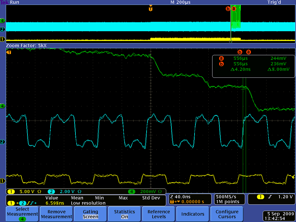
|
|
241
|
Mon Apr 22 15:33:28 2013 |
Benjamin LeGeyt | effect of jitter/alignment between SRCLK and ADC clock | Hello!
let me apologize in advance if this has already been covered somewhere and I missed it.
I have a question about a statement made regarding the ADC clock in the evaluation board v4.0 manual. At the bottom or page 23 there is a mention of jitter between the SRCLK signal and the ADC clock causing a baseline variation in the sampled output of up to a few mV. Is there any more information out there about this? I find this confusing for the following reason: If the DRS output has mostly settled after 28ns and the signal that is being sampled is a DC signal, I don't understand why an aperture jitter in the sampling ADC should cause a voltage error in the measured signal. I already know about the possibility of noise spikes every 32 samples if these clocks are not properly aligned, though I don't know the origin of those spikes. are these two things related?
Many Thanks!
|
|
240
|
Fri Apr 12 08:38:17 2013 |
Stefan Ritt | code/details for optimal DRS4 timing calibration? |
| Bill Ashmanskas wrote: |
|
Hi Stefan,
Is either some example code or a detailed written description available for the improved DRS4 timing-calibration algorithm described by Daniel Stricker-Shaver at MIC 2012? I think you told me that you had verified the results with your own test set-up, so I figure there must be at least two sets of code in existence to implement this calibration. (I have Daniel's presentation slides.)
I managed to find a ping-pong distribution of cell widths that looks quite similar to that shown in Daniel's slides, using an algorithm similar to the technique one uses to find radial offsets in a tracking chamber (i.e. using residuals weighted by track slope), but I'd rather use the method with which you and Daniel have already found good results. (The attached graph shows in black the histogram of cell widths for essentially the algorithm used in DRS.cpp/DRSBoard::AnalyzeWF, and in blue the histogram of cell widths extracted from the slope-weighted residuals for a periodic reference signal.)
By the way, since Daniel finds a FWHM coincidence-timing resolution around 20-25ps at 5 GSPS (for perfectly identical pulses), should I expect a FWHM resolution (for synthesized, ideal pulses) of around 50-65ps at 2 GSPS?
(I'm posting here instead of writing you both privately because I figure there may be broader interest in Daniel's algorithm.)
-Bill
|
Hi Bill,
there are several reasons why we have not yet published Daniel's method (I'm in constant contact with him).
1. The method still changes, becomes simpler and more accurate. Originally he used sine waves with varying frequency, which you only get from an external function oscillator. Currently, we found that a single frequency could do a similar, maybe even better job. The current result is much better than the 20-25ps quoted at MIC 2012.
2. Daniel found out that for the ultimate resolution you have to calibrate each channel inside a chip separately. I do understand in meantime the reason for that. So I plan for a V5 evaluation board, which contains means of sending a log-jitter clock to all channels. This board is in test phase and will be made available once it's working as expected.
So my plan is to finish the V5 board and implement the best possible timing calibration on it. Daniel achieved already <5 ps RMS (!) independent of the delay between the two optimal pulses (up to 50 ns). This is actually better than what you can do with a high-end oscilloscope, since scopes have internal interleaving and similar problems due to aliasing etc. than the DRS chip, but scope manufacturers do not put such an emphasis on accurate timing measurements. Once we can reproduce the 5 ps result with the evaluation board, we will publish it. When we found the optimal method, we plan to write a paper about it and explain everything in great detail. We will also be at Seoul for MIC 2013. I'm topic convener there for the session "Digitalization, Acquisition, and Signal Processing Technologies". So probably we will put the DRS4 timing talk there, since it's of more general interest not only to medical applications (and honestly, for a 150 ps TOF-PET you do not need a 5 ps electronics resolution). So stay tuned!
/Stefan |
|
239
|
Fri Apr 12 08:25:05 2013 |
Stefan Ritt | cascading -- DRS4 Osci.cpp & DRS.cpp |
| Jill Russek wrote: |
|
| Stefan Ritt wrote: |
|
| Jill Russek wrote: |
|
Stefan, thanks for your help so far. If I go with your plan A of just modifying drs_exam.cpp, is there a quick way to get it to save the data from the wave, like how osci.cpp spits out an xml file? (Ignoring the cascading aspect for now)
Thanks again :)
/Jill
|
Well, you have to learn C programming, I won't do it for you. drs_exam.cpp contains already code to write to the ASCII file data.txt, so you just can use that or modify it to your needs.
/Stefan
|
Ha! So then the answer is no, there isn't a ready made function/method to pull out the timing and voltage, like how it was done in osci.cpp. That's all I wanted to know. (Not whether you would write it for me! Only trying to save time!) Thanks!
/Jill
|
You misunderstood. The answer is yes. drs_exam.cpp contains already code to write to an ASCII file. If you actually look into the file, you see:
f = fopen("data.txt", "w");
...
b->GetTime(0, b->GetTriggerCell(0), time_array);
...
b->GetWave(0, 0, wave_array[0]);
...
fprintf(f, "%5.2f %6.2f\n", time_array[i], wave_array[0][i]);
which actually pulls out the timing and voltage and writes it to the file. |
|
238
|
Thu Apr 11 23:32:57 2013 |
Jill Russek | cascading -- DRS4 Osci.cpp & DRS.cpp |
| Stefan Ritt wrote: |
|
| Jill Russek wrote: |
|
| Stefan Ritt wrote: |
|
| Jill Russek wrote: |
|
Would it be possible to just hardcode a few lines in the SetChannelConfig in DRS.cpp method as such:
fChannelConfig = 0x01; //gives me eight
d = fChannelConfig | (fDominoMode << 8) | (1 << 9) | (fWSRLoop << 10) | (0xF8 << 8);
Write(T_CTRL, REG_CHANNEL_CONFIG, &d, 2);
fChannelDepth = 8 * (fDecimation ? kNumberOfBins/2 : kNumberOfBins);// gives eight times the bins
then modify the GetWave method/function to include another else if statement similar to "else if (fChannelCascading == 2) {" but would be modifidied for fChannelCascading == 8?
By, "But then you will hit the hard-wired limit in Osci.cpp" do you mean hard-coded? Would changing the hard code just amount to resizing all of the arrays, and replacing all the '2*kNumberBins" with '8*kNumberBins' ?
I'm afraid of drs_exam.cpp because it doesn't come with all the perks of Osci.cpp. It seems less daunting to just modify Osci.cpp then to try understanding everything I need to include in drs_exam.cpp because I'm also using an external trigger, and saving the waveform to an external text file.
Thanks!
/Jill
|
Sure it would be possible to code it, but it's not just a few lines. Besides Osci.cpp you have to massage DOScreen.cpp, Measurement.cpp and probably more since they all rely on the array size of the waveform. So if I would do it it would take me probably a couple of days including the debugging, which I don't have right now. Furthermore, as I said you have to combine all eight channels properly. For two channels, it's already pretty complicated (see lines 3537+ in DRS.cpp). I had to make myself a visual scheme in order to understand it correctly, which I attached. For eight channels, the write shift register (WSR) can have values 0-7, depending in which channel you got a trigger. Then you have to sort it out again to get one linear array with the proper order of the fragments. So you see, it's not just changing a few lines of code. In principle it's possible, but it's lots of work.
Best regards,
Stefan
|
Stefan, thanks for your help so far. If I go with your plan A of just modifying drs_exam.cpp, is there a quick way to get it to save the data from the wave, like how osci.cpp spits out an xml file? (Ignoring the cascading aspect for now)
Thanks again :)
/Jill
|
Well, you have to learn C programming, I won't do it for you. drs_exam.cpp contains already code to write to the ASCII file data.txt, so you just can use that or modify it to your needs.
/Stefan
|
Ha! So then the answer is no, there isn't a ready made function/method to pull out the timing and voltage, like how it was done in osci.cpp. That's all I wanted to know. (Not whether you would write it for me! Only trying to save time!) Thanks!
/Jill |
|
237
|
Thu Apr 11 22:41:13 2013 |
Bill Ashmanskas | code/details for optimal DRS4 timing calibration? | Hi Stefan,
Is either some example code or a detailed written description available for the improved DRS4 timing-calibration algorithm described by Daniel Stricker-Shaver at MIC 2012? I think you told me that you had verified the results with your own test set-up, so I figure there must be at least two sets of code in existence to implement this calibration. (I have Daniel's presentation slides.)
I managed to find a ping-pong distribution of cell widths that looks quite similar to that shown in Daniel's slides, using an algorithm similar to the technique one uses to find radial offsets in a tracking chamber (i.e. using residuals weighted by track slope), but I'd rather use the method with which you and Daniel have already found good results. (The attached graph shows in black the histogram of cell widths for essentially the algorithm used in DRS.cpp/DRSBoard::AnalyzeWF, and in blue the histogram of cell widths extracted from the slope-weighted residuals for a periodic reference signal.)
By the way, since Daniel finds a FWHM coincidence-timing resolution around 20-25ps at 5 GSPS (for perfectly identical pulses), should I expect a FWHM resolution (for synthesized, ideal pulses) of around 50-65ps at 2 GSPS?
(I'm posting here instead of writing you both privately because I figure there may be broader interest in Daniel's algorithm.)
-Bill
|
| Attachment 1: tcalib.png
|

|
|
236
|
Thu Apr 11 08:39:12 2013 |
Stefan Ritt | cascading -- DRS4 Osci.cpp & DRS.cpp |
| Jill Russek wrote: |
|
| Stefan Ritt wrote: |
|
| Jill Russek wrote: |
|
Would it be possible to just hardcode a few lines in the SetChannelConfig in DRS.cpp method as such:
fChannelConfig = 0x01; //gives me eight
d = fChannelConfig | (fDominoMode << 8) | (1 << 9) | (fWSRLoop << 10) | (0xF8 << 8);
Write(T_CTRL, REG_CHANNEL_CONFIG, &d, 2);
fChannelDepth = 8 * (fDecimation ? kNumberOfBins/2 : kNumberOfBins);// gives eight times the bins
then modify the GetWave method/function to include another else if statement similar to "else if (fChannelCascading == 2) {" but would be modifidied for fChannelCascading == 8?
By, "But then you will hit the hard-wired limit in Osci.cpp" do you mean hard-coded? Would changing the hard code just amount to resizing all of the arrays, and replacing all the '2*kNumberBins" with '8*kNumberBins' ?
I'm afraid of drs_exam.cpp because it doesn't come with all the perks of Osci.cpp. It seems less daunting to just modify Osci.cpp then to try understanding everything I need to include in drs_exam.cpp because I'm also using an external trigger, and saving the waveform to an external text file.
Thanks!
/Jill
|
Sure it would be possible to code it, but it's not just a few lines. Besides Osci.cpp you have to massage DOScreen.cpp, Measurement.cpp and probably more since they all rely on the array size of the waveform. So if I would do it it would take me probably a couple of days including the debugging, which I don't have right now. Furthermore, as I said you have to combine all eight channels properly. For two channels, it's already pretty complicated (see lines 3537+ in DRS.cpp). I had to make myself a visual scheme in order to understand it correctly, which I attached. For eight channels, the write shift register (WSR) can have values 0-7, depending in which channel you got a trigger. Then you have to sort it out again to get one linear array with the proper order of the fragments. So you see, it's not just changing a few lines of code. In principle it's possible, but it's lots of work.
Best regards,
Stefan
|
Stefan, thanks for your help so far. If I go with your plan A of just modifying drs_exam.cpp, is there a quick way to get it to save the data from the wave, like how osci.cpp spits out an xml file? (Ignoring the cascading aspect for now)
Thanks again :)
/Jill
|
Well, you have to learn C programming, I won't do it for you. drs_exam.cpp contains already code to write to the ASCII file data.txt, so you just can use that or modify it to your needs.
/Stefan |
|
235
|
Wed Apr 10 22:41:21 2013 |
Jill Russek | cascading -- DRS4 Osci.cpp & DRS.cpp |
| Stefan Ritt wrote: |
|
| Jill Russek wrote: |
|
Would it be possible to just hardcode a few lines in the SetChannelConfig in DRS.cpp method as such:
fChannelConfig = 0x01; //gives me eight
d = fChannelConfig | (fDominoMode << 8) | (1 << 9) | (fWSRLoop << 10) | (0xF8 << 8);
Write(T_CTRL, REG_CHANNEL_CONFIG, &d, 2);
fChannelDepth = 8 * (fDecimation ? kNumberOfBins/2 : kNumberOfBins);// gives eight times the bins
then modify the GetWave method/function to include another else if statement similar to "else if (fChannelCascading == 2) {" but would be modifidied for fChannelCascading == 8?
By, "But then you will hit the hard-wired limit in Osci.cpp" do you mean hard-coded? Would changing the hard code just amount to resizing all of the arrays, and replacing all the '2*kNumberBins" with '8*kNumberBins' ?
I'm afraid of drs_exam.cpp because it doesn't come with all the perks of Osci.cpp. It seems less daunting to just modify Osci.cpp then to try understanding everything I need to include in drs_exam.cpp because I'm also using an external trigger, and saving the waveform to an external text file.
Thanks!
/Jill
|
Sure it would be possible to code it, but it's not just a few lines. Besides Osci.cpp you have to massage DOScreen.cpp, Measurement.cpp and probably more since they all rely on the array size of the waveform. So if I would do it it would take me probably a couple of days including the debugging, which I don't have right now. Furthermore, as I said you have to combine all eight channels properly. For two channels, it's already pretty complicated (see lines 3537+ in DRS.cpp). I had to make myself a visual scheme in order to understand it correctly, which I attached. For eight channels, the write shift register (WSR) can have values 0-7, depending in which channel you got a trigger. Then you have to sort it out again to get one linear array with the proper order of the fragments. So you see, it's not just changing a few lines of code. In principle it's possible, but it's lots of work.
Best regards,
Stefan
|
Stefan, thanks for your help so far. If I go with your plan A of just modifying drs_exam.cpp, is there a quick way to get it to save the data from the wave, like how osci.cpp spits out an xml file? (Ignoring the cascading aspect for now)
Thanks again :)
/Jill |
|
234
|
Mon Apr 8 18:11:02 2013 |
Dmitry Hits | binary to root | Hi,
Does anyone has a program that converts a binary file from drsosc output to a ROOT tree format?
Thank you,
Dmitry. |
|
233
|
Fri Apr 5 08:54:37 2013 |
Stefan Ritt | cascading -- DRS4 Osci.cpp & DRS.cpp |
| Jill Russek wrote: |
|
Would it be possible to just hardcode a few lines in the SetChannelConfig in DRS.cpp method as such:
fChannelConfig = 0x01; //gives me eight
d = fChannelConfig | (fDominoMode << 8) | (1 << 9) | (fWSRLoop << 10) | (0xF8 << 8);
Write(T_CTRL, REG_CHANNEL_CONFIG, &d, 2);
fChannelDepth = 8 * (fDecimation ? kNumberOfBins/2 : kNumberOfBins);// gives eight times the bins
then modify the GetWave method/function to include another else if statement similar to "else if (fChannelCascading == 2) {" but would be modifidied for fChannelCascading == 8?
By, "But then you will hit the hard-wired limit in Osci.cpp" do you mean hard-coded? Would changing the hard code just amount to resizing all of the arrays, and replacing all the '2*kNumberBins" with '8*kNumberBins' ?
I'm afraid of drs_exam.cpp because it doesn't come with all the perks of Osci.cpp. It seems less daunting to just modify Osci.cpp then to try understanding everything I need to include in drs_exam.cpp because I'm also using an external trigger, and saving the waveform to an external text file.
Thanks!
/Jill
|
Sure it would be possible to code it, but it's not just a few lines. Besides Osci.cpp you have to massage DOScreen.cpp, Measurement.cpp and probably more since they all rely on the array size of the waveform. So if I would do it it would take me probably a couple of days including the debugging, which I don't have right now. Furthermore, as I said you have to combine all eight channels properly. For two channels, it's already pretty complicated (see lines 3537+ in DRS.cpp). I had to make myself a visual scheme in order to understand it correctly, which I attached. For eight channels, the write shift register (WSR) can have values 0-7, depending in which channel you got a trigger. Then you have to sort it out again to get one linear array with the proper order of the fragments. So you see, it's not just changing a few lines of code. In principle it's possible, but it's lots of work.
Best regards,
Stefan |
| Attachment 1: Screen_Shot_2013-04-05_at_8.51.53_.png
|

|
|
232
|
Fri Apr 5 02:21:33 2013 |
Jill Russek | cascading -- DRS4 Osci.cpp & DRS.cpp |
| Stefan Ritt wrote: |
|
| Jill Russek wrote: |
|
All I'm trying to do is cascade one input signal, though all available channels, so that I end up with 8*1024 bins per event.
Here is the read out on my board/chip:
Mezz. Board index: 0
DRS type: DRS4
Board type: 8
Serial number: 2249
Firmware revision: 17662
Temperature: 35.2 C
Input range: -0.5V...0.5V
Calibrated range: -0.5V...0.5V
Calibrated frequency: 5.120 GHz
Status reg.: 0000001A
Control reg.: 00000010
DMODE circular
Trigger bus: 00000000
Frequency: 5.120 GHz
What I've tried thus far:
In Osci.cpp, in the method/function SelectSource(int board, int firstChannel, int chnSection), I added a line.. (in bold)
//----------------------------------------------------------------------------------------------------------------------------------------------
if (b->GetBoardType() == 5 || b->GetBoardType() == 7 || b->GetBoardType() == 8) {


                                     if (chnSection == 2)

                                        b->SetChannelConfig(0, 8, 4);

                                     //added

                                     else if(chnSection == 1)

                                         b->SetChannelConfig(0, 8, 2);

                                     //added

                                     else

                                        b->SetChannelConfig(0, 8, 8);
//----------------------------------------------------------------------------------------------------------------------------------------------
I've also tried doing settings such as SetChannelConfig(0, 8, 1); , SetChannelConfig(0, 8, 2); , SetChannelConfig(0, 1, 2); , etc..
Which always ends up making the run fail.. and sometimes I get index errors..
As far as I understanding the program now, this is what I know:
fChannelCascading determines getChannelCascading,

                        this determines the  if (casc == 2) line in configDialogue.cpp, which sets:

                         b->SetChannelConfig(config, 8, 4);


                        fChannelCascading is being set by:

                         switch (nConfigChannels) {

                              case 1:

                                 fChannelConfig = 0x01;

                                 fChannelCascading = 8;

                                 break;

                              case 2:

                                 fChannelConfig = 0x11;

                                 fChannelCascading = 4;

                                 break;

                              case 4:

                                 fChannelConfig = 0x55;

                                 fChannelCascading = 2;

                                 break;

                              case 8:

                                 fChannelConfig = 0xFF;

                                 fChannelCascading = 1;

                                 break;

                              default:

                                 printf("Invalid channel configuration\n");

                                 return 0;

                              }


                        which is being set by nConfigChannels in DRS.cpp, in the method:

                        SetChannelConfig(int firstChannel, int lastChannel, int nConfigChannels)
SetChannelConfig is being called in the ConfigDialogue.cpp, but the default Osci program is such that you can't do a configuration for a cascade of one signal using all the channels. At least, not that I am aware of.
So what buttons do I need to enable, or what do I need to call, or write, so that I can cascade a signal to end up with 8*1024 bins per event?
This has had me going in circles for weeks, so thank you for your help!!!!
|
Sorry for my late reply, I was away for some days.
To use channel cascading, you have to physically connect one input to all eight channels. This is not possible with the evaluation board, you have to make your own board. What you could do however is to split a signal externally and feed it to all four inputs, given that the signal delay is the same for every channel. But then you will hit the hard-wired limit in Osci.cpp. This code was never foreseen to cover 8*1024 bins (since it does not make much sense with the evaluation board). Some arrays are only 2*1024 bins wide, so you would have to rewrite code at many places.
The easiest way to get what you want is to modify drs_exam.cpp. You need SetChannelConfig(0, 8, 1) as you realised correctly, and then you have to retrieve all 8 channels via b->GetWave() and concatenate them correctly.
/Stefan
|
Would it be possible to just hardcode a few lines in the SetChannelConfig in DRS.cpp method as such:
fChannelConfig = 0x01; //gives me eight
d = fChannelConfig | (fDominoMode << 8) | (1 << 9) | (fWSRLoop << 10) | (0xF8 << 8);
Write(T_CTRL, REG_CHANNEL_CONFIG, &d, 2);
fChannelDepth = 8 * (fDecimation ? kNumberOfBins/2 : kNumberOfBins);// gives eight times the bins
then modify the GetWave method/function to include another else if statement similar to "else if (fChannelCascading == 2) {" but would be modifidied for fChannelCascading == 8?
By, "But then you will hit the hard-wired limit in Osci.cpp" do you mean hard-coded? Would changing the hard code just amount to resizing all of the arrays, and replacing all the '2*kNumberBins" with '8*kNumberBins' ?
I'm afraid of drs_exam.cpp because it doesn't come with all the perks of Osci.cpp. It seems less daunting to just modify Osci.cpp then to try understanding everything I need to include in drs_exam.cpp because I'm also using an external trigger, and saving the waveform to an external text file.
Thanks!
/Jill
|
|
231
|
Thu Apr 4 11:32:21 2013 |
Stefan Ritt | cascading -- DRS4 Osci.cpp & DRS.cpp |
| Jill Russek wrote: |
|
All I'm trying to do is cascade one input signal, though all available channels, so that I end up with 8*1024 bins per event.
Here is the read out on my board/chip:
Mezz. Board index: 0
DRS type: DRS4
Board type: 8
Serial number: 2249
Firmware revision: 17662
Temperature: 35.2 C
Input range: -0.5V...0.5V
Calibrated range: -0.5V...0.5V
Calibrated frequency: 5.120 GHz
Status reg.: 0000001A
Control reg.: 00000010
DMODE circular
Trigger bus: 00000000
Frequency: 5.120 GHz
What I've tried thus far:
In Osci.cpp, in the method/function SelectSource(int board, int firstChannel, int chnSection), I added a line.. (in bold)
//----------------------------------------------------------------------------------------------------------------------------------------------
if (b->GetBoardType() == 5 || b->GetBoardType() == 7 || b->GetBoardType() == 8) {


                         if (chnSection == 2)

                            b->SetChannelConfig(0, 8, 4);

                         //added

                         else if(chnSection == 1)

                             b->SetChannelConfig(0, 8, 2);

                         //added

                         else

                            b->SetChannelConfig(0, 8, 8);
//----------------------------------------------------------------------------------------------------------------------------------------------
I've also tried doing settings such as SetChannelConfig(0, 8, 1); , SetChannelConfig(0, 8, 2); , SetChannelConfig(0, 1, 2); , etc..
Which always ends up making the run fail.. and sometimes I get index errors..
As far as I understanding the program now, this is what I know:
fChannelCascading determines getChannelCascading,

            this determines the  if (casc == 2) line in configDialogue.cpp, which sets:

             b->SetChannelConfig(config, 8, 4);


            fChannelCascading is being set by:

             switch (nConfigChannels) {

                  case 1:

                     fChannelConfig = 0x01;

                     fChannelCascading = 8;

                     break;

                  case 2:

                     fChannelConfig = 0x11;

                     fChannelCascading = 4;

                     break;

                  case 4:

                     fChannelConfig = 0x55;

                     fChannelCascading = 2;

                     break;

                  case 8:

                     fChannelConfig = 0xFF;

                     fChannelCascading = 1;

                     break;

                  default:

                     printf("Invalid channel configuration\n");

                     return 0;

                  }


            which is being set by nConfigChannels in DRS.cpp, in the method:

            SetChannelConfig(int firstChannel, int lastChannel, int nConfigChannels)
SetChannelConfig is being called in the ConfigDialogue.cpp, but the default Osci program is such that you can't do a configuration for a cascade of one signal using all the channels. At least, not that I am aware of.
So what buttons do I need to enable, or what do I need to call, or write, so that I can cascade a signal to end up with 8*1024 bins per event?
This has had me going in circles for weeks, so thank you for your help!!!!
|
Sorry for my late reply, I was away for some days.
To use channel cascading, you have to physically connect one input to all eight channels. This is not possible with the evaluation board, you have to make your own board. What you could do however is to split a signal externally and feed it to all four inputs, given that the signal delay is the same for every channel. But then you will hit the hard-wired limit in Osci.cpp. This code was never foreseen to cover 8*1024 bins (since it does not make much sense with the evaluation board). Some arrays are only 2*1024 bins wide, so you would have to rewrite code at many places.
The easiest way to get what you want is to modify drs_exam.cpp. You need SetChannelConfig(0, 8, 1) as you realised correctly, and then you have to retrieve all 8 channels via b->GetWave() and concatenate them correctly.
/Stefan |
|
230
|
Thu Apr 4 11:21:04 2013 |
Stefan Ritt | Differences in Source Code |
| Georg Winner wrote: |
|
I have noticed some differences in the source code between Windows (4.0.0) and Linux (4.0.1) Version.
drs_exam.cpp: In the windows version when setting the trigger there is no part "if (b->GetBoardType() == 8) {...} else {...}" like in Linux version. So under Windows drs_exam does not start readout of DRS 4 Evalutation Board V4, because it does not get the trigger, under linux the board can be read out succesfull. I have found out, that adding the missing part solves the problem for the windows version.
drs.cpp (Windows Version), line 2101, function "int DRSBoard::SetTriggerDelayNs(int delay)":
There is no operation which calculates the variable "fTriggerDelayNs" out of variable "ticks" like in function "int DRSBoard::SetTriggerDelayPercent(int delay)" (Line 2073). So "fTriggerDelayNs" can get diverse values when using one of the Trigger Setting Functions. Was this intended?
|
Thanks for reporting the problem in drs_exam.cpp. The windows and linux versions sometimes differ a bit. I'm working right now on a complete new version, wich will bring both together again.
Concerning fTriggerDelayNs and ticks, they are correlated. One tick is a single delay unit in the FPGA. On the newest boards the unit is 4.8ns long. So
ticks = fTriggerDelayNs / 4.8
fTriggerDelayNs = ticks * 4.8
fTriggerDelayNs gets set at the first line of SetTriggerDelayNs:
int DRSBoard::SetTriggerDelayNs(int delay)
/* set trigger delay in nanoseconds */
{
short ticks, reg;
fTriggerDelayNs = delay;
So I cannot see how fTriggerDelayNS should get diverse values?
|
|
229
|
Tue Mar 26 01:17:59 2013 |
Jill Russek | cascading -- DRS4 Osci.cpp & DRS.cpp |
All I'm trying to do is cascade one input signal, though all available channels, so that I end up with 8*1024 bins per event.
Here is the read out on my board/chip:
Mezz. Board index: 0
DRS type: DRS4
Board type: 8
Serial number: 2249
Firmware revision: 17662
Temperature: 35.2 C
Input range: -0.5V...0.5V
Calibrated range: -0.5V...0.5V
Calibrated frequency: 5.120 GHz
Status reg.: 0000001A
Control reg.: 00000010
DMODE circular
Trigger bus: 00000000
Frequency: 5.120 GHz
What I've tried thus far:
In Osci.cpp, in the method/function SelectSource(int board, int firstChannel, int chnSection), I added a line.. (in bold)
//----------------------------------------------------------------------------------------------------------------------------------------------
if (b->GetBoardType() == 5 || b->GetBoardType() == 7 || b->GetBoardType() == 8) {


             if (chnSection == 2)

                b->SetChannelConfig(0, 8, 4);

             //added

             else if(chnSection == 1)

                 b->SetChannelConfig(0, 8, 2);

             //added

             else

                b->SetChannelConfig(0, 8, 8);
//----------------------------------------------------------------------------------------------------------------------------------------------
I've also tried doing settings such as SetChannelConfig(0, 8, 1); , SetChannelConfig(0, 8, 2); , SetChannelConfig(0, 1, 2); , etc..
Which always ends up making the run fail.. and sometimes I get index errors..
As far as I understanding the program now, this is what I know:
fChannelCascading determines getChannelCascading,

this determines the  if (casc == 2) line in configDialogue.cpp, which sets:

 b->SetChannelConfig(config, 8, 4);


fChannelCascading is being set by:

 switch (nConfigChannels) {

      case 1:

         fChannelConfig = 0x01;

         fChannelCascading = 8;

         break;

      case 2:

         fChannelConfig = 0x11;

         fChannelCascading = 4;

         break;

      case 4:

         fChannelConfig = 0x55;

         fChannelCascading = 2;

         break;

      case 8:

         fChannelConfig = 0xFF;

         fChannelCascading = 1;

         break;

      default:

         printf("Invalid channel configuration\n");

         return 0;

      }


which is being set by nConfigChannels in DRS.cpp, in the method:

SetChannelConfig(int firstChannel, int lastChannel, int nConfigChannels)
SetChannelConfig is being called in the ConfigDialogue.cpp, but the default Osci program is such that you can't do a configuration for a cascade of one signal using all the channels. At least, not that I am aware of.
So what buttons do I need to enable, or what do I need to call, or write, so that I can cascade a signal to end up with 8*1024 bins per event?
This has had me going in circles for weeks, so thank you for your help!!!!
|
|
228
|
Mon Mar 25 11:12:53 2013 |
Georg Winner | Differences in Source Code | I have noticed some differences in the source code between Windows (4.0.0) and Linux (4.0.1) Version.
drs_exam.cpp: In the windows version when setting the trigger there is no part "if (b->GetBoardType() == 8) {...} else {...}" like in Linux version. So under Windows drs_exam does not start readout of DRS 4 Evalutation Board V4, because it does not get the trigger, under linux the board can be read out succesfull. I have found out, that adding the missing part solves the problem for the windows version.
drs.cpp (Windows Version), line 2101, function "int DRSBoard::SetTriggerDelayNs(int delay)":
There is no operation which calculates the variable "fTriggerDelayNs" out of variable "ticks" like in function "int DRSBoard::SetTriggerDelayPercent(int delay)" (Line 2073). So "fTriggerDelayNs" can get diverse values when using one of the Trigger Setting Functions. Was this intended?
|
|
227
|
Wed Mar 6 13:08:03 2013 |
Stefan Ritt | Chip Test - Cell Error |
| Georg Winner wrote: |
|
When starting Chip Test in DRS Command Line Interface, I receive the following message:
Cell error on channel 1, cell 5: -154.4 mV instead 0 mV
Chip Error!
What does this mean? The maximal peak-to-peak Amplitude given to channel was for a short time 10V.
The graphical interface shows no artefacts when using channel 1.
|
The "Chip Test" command is made for a special test board we use for chip testing. This command will not work with the evaluation board, since only four of the 8 DRS channels are connected there. So just ignore it and verify the board functionality by looking at the graphical interface.
/Stefan |
|
226
|
Wed Mar 6 12:37:14 2013 |
Stefan Ritt | DRS4- analog pulse counting |
| Osip Lishilin wrote: |
|
Hello, Stefan. Have you implemented pulse counting yet?
Best, Osip.
|
Nope. |
|
225
|
Wed Mar 6 12:35:38 2013 |
Osip Lishilin | DRS4- analog pulse counting | Hello, Stefan. Have you implemented pulse counting yet?
Best, Osip. |
|
224
|
Thu Feb 28 12:58:44 2013 |
Stefan Ritt | clock and trigger outs | > Hi,
> I am considering using the DRS4 evaluation board as an ADC card for the wire chamber in the physics lab (VP) experiment at ETH. However, the wire
> chamber has 8 outputs, so I would need to have two of such boards. Is it possible to synchronise them, online or offline? From the website, it looks
> like yes, but the documentation says that these features (trigger and clock out) may not have been implemented in firmware yet. Could you tell me
> the status?
>
> Thank you very much,
>
> Dmitry.
I'm right now working on it. If you only need 2-3 ns accuracy between the two boards then you can do this already now without firmware upgrade. The software for this is in principle ready, but I have to
finish the documentation. Since I'm on a business travel right now this might take me some time (weeks?).
If you want better timing (O(100ps)) between the boards, then you will need a firmware update. Or you wait until we ship boards with the new firmware. I will announce this through this forum.
Stefan |
|
223
|
Thu Feb 28 10:47:14 2013 |
Dmitry Hits | clock and trigger outs | Hi,
I am considering using the DRS4 evaluation board as an ADC card for the wire chamber in the physics lab (VP) experiment at ETH. However, the wire
chamber has 8 outputs, so I would need to have two of such boards. Is it possible to synchronise them, online or offline? From the website, it looks
like yes, but the documentation says that these features (trigger and clock out) may not have been implemented in firmware yet. Could you tell me
the status?
Thank you very much,
Dmitry. |
|
222
|
Wed Feb 27 13:47:32 2013 |
Georg Winner | Chip Test - Cell Error | When starting Chip Test in DRS Command Line Interface, I receive the following message:
Cell error on channel 1, cell 5: -154.4 mV instead 0 mV
Chip Error!
What does this mean? The maximal peak-to-peak Amplitude given to channel was for a short time 10V.
The graphical interface shows no artefacts when using channel 1.
|
|
220
|
Fri Feb 22 11:56:57 2013 |
Stefan Ritt | DRS4 trigger, different polarity |
| Yury Golod wrote: |
|
I need to synchronize two signals. These signals have a different polarity.
I can set triggers on different levels. But I can't set different polarity of triggers.
Now I can set (T1 and T2), I need to set (T1 and (not T2))
Is it possible?
d->SetTriggerLevel(-0.4,0.4,0.0,0.0,false);
d->EnableTrigger(1, 0); // Enable trigger
d->SetTriggerSource(1<<8 | 1<<9); // T1 and T2
file DRS.cpp:
int DRSBoard::SetTriggerLevel(double voltage1,double voltage2, double voltage3,double voltage4,bool negative)
{
…
SetDAC(fDAC_TLEVEL1, voltage1/2 + 0.8);
SetDAC(fDAC_TLEVEL2, voltage2/2 + 0.8);
…
|
There is no way to select different polarities, it is not implemented in the firmware. Like your digital oscilloscope has also only one polarity switch.
The only way to do it is to use a (passive) inverter, so that you have two signals of the same polarity. Something like this:
http://www.phillipsscientific.com/pdf/460ds.pdf
|
|
219
|
Fri Feb 22 11:46:17 2013 |
Yury Golod | DRS4 trigger, different polarity |
I need to synchronize two signals. These signals have a different polarity.
I can set triggers on different levels. But I can't set different polarity of triggers.
Now I can set (T1 and T2), I need to set (T1 and (not T2))
Is it possible?
d->SetTriggerLevel(-0.4,0.4,0.0,0.0,false);
d->EnableTrigger(1, 0); // Enable trigger
d->SetTriggerSource(1<<8 | 1<<9); // T1 and T2
file DRS.cpp:
int DRSBoard::SetTriggerLevel(double voltage1,double voltage2, double voltage3,double voltage4,bool negative)
{
…
SetDAC(fDAC_TLEVEL1, voltage1/2 + 0.8);
SetDAC(fDAC_TLEVEL2, voltage2/2 + 0.8);
…
|
|
218
|
Wed Feb 13 17:03:53 2013 |
Stefan Ritt | Nonuniform sampling |
| Martin Petriska wrote: |
|
Are there any plans to include reconstruction of nonuniform sampling in DRS4 to get uniformly sampled data?
Im now reading article IEEE Trans on Circ. ans Systems I, Vol.55 No.8 sept. 2008 Reconstruction of Nonuniformly Sampled Bandlimited Signals Usinga Differentiator–Multiplier Cascade by Stefan Tertinek and Christian Vogel
and plan to implement it, but may be somebody has it done before me.
|
Interesting paper. I was not aware of this method. Sounds interesting. AFAIK, nobody has implemented it so far.
My (old) plan was to linearly interpolate samples (something you could do in an FPGA as well), but this will introduce (small) errors. The next best thing would be to do some spline interpolation, but this is time consuming and not suited for an FPGA.
If you get good results with the method above, please let others know about it.
/Stefan |
|
217
|
Wed Feb 13 16:58:40 2013 |
Martin Petriska | Nonuniform sampling | Are there any plans to include reconstruction of nonuniform sampling in DRS4 to get uniformly sampled data?
Im now reading article IEEE Trans on Circ. ans Systems I, Vol.55 No.8 sept. 2008 Reconstruction of Nonuniformly Sampled Bandlimited Signals Usinga Differentiator–Multiplier Cascade by Stefan Tertinek and Christian Vogel
and plan to implement it, but may be somebody has it done before me.
|
|
216
|
Tue Feb 5 14:38:35 2013 |
Stefan Ritt | variation of sampling capacitors |
| Jinhong Wang wrote: |
|
Hi Dr. Stefan,
So the sampling capacitors store the input voltage instead of the charge. What about the readout circuits? I saw there is a buffer followed each sampling capacitor. Do you buffer the charge (like a charge sensitive amplifier) or the voltage? From Fig.12, 14 in datasheet, it seems most probably the readout is a charging or discharging of a capacitor. Could you please add some comments on this?
Cheers,
Jinhong
|
The buffer buffers the voltage, not the charge. The curves in Fig. 12, 14 indicate that the voltage followers take some time until they settle.
Stefan |
|
215
|
Fri Feb 1 17:43:48 2013 |
Jinhong Wang | variation of sampling capacitors |
| Jinhong Wang wrote: |
|
| Stefan Ritt wrote: |
|
| Jinhong Wang wrote: |
|
Hi Stefan,
A quick question, what is the typical variation of the sampling capacitors in DRS4? Will this variation be significant to affect your sampling result?
Best,
Jinhong
|
The capacitors sample the input voltage, not the charge, so the actual size of the capacitors does not matter on first order (the variations might be in the order of 5%). A bigger effect is the variation of the analog switches in the front of the capacitors, which is about 15%. So the actual bandwidth each cell sees varies by maybe 20% (given by the R and the C), but this comes only into play when sampling steep edges.
Stefan
|
Great to know this! Thanks~
Jinhong
|
Hi Dr. Stefan,
So the sampling capacitors store the input voltage instead of the charge. What about the readout circuits? I saw there is a buffer followed each sampling capacitor. Do you buffer the charge (like a charge sensitive amplifier) or the voltage? From Fig.12, 14 in datasheet, it seems most probably the readout is a charging or discharging of a capacitor. Could you please add some comments on this?
Cheers,
Jinhong |
|
214
|
Thu Dec 27 18:15:14 2012 |
Jinhong Wang | variation of sampling capacitors |
| Stefan Ritt wrote: |
|
| Jinhong Wang wrote: |
|
Hi Stefan,
A quick question, what is the typical variation of the sampling capacitors in DRS4? Will this variation be significant to affect your sampling result?
Best,
Jinhong
|
The capacitors sample the input voltage, not the charge, so the actual size of the capacitors does not matter on first order (the variations might be in the order of 5%). A bigger effect is the variation of the analog switches in the front of the capacitors, which is about 15%. So the actual bandwidth each cell sees varies by maybe 20% (given by the R and the C), but this comes only into play when sampling steep edges.
Stefan
|
Great to know this! Thanks~
Jinhong |
|
213
|
Thu Dec 27 09:49:17 2012 |
Stefan Ritt | variation of sampling capacitors |
| Jinhong Wang wrote: |
|
Hi Stefan,
A quick question, what is the typical variation of the sampling capacitors in DRS4? Will this variation be significant to affect your sampling result?
Best,
Jinhong
|
The capacitors sample the input voltage, not the charge, so the actual size of the capacitors does not matter on first order (the variations might be in the order of 5%). A bigger effect is the variation of the analog switches in the front of the capacitors, which is about 15%. So the actual bandwidth each cell sees varies by maybe 20% (given by the R and the C), but this comes only into play when sampling steep edges.
Stefan |
|
212
|
Thu Dec 27 00:12:12 2012 |
Jinhong Wang | variation of sampling capacitors | Hi Stefan,
A quick question, what is the typical variation of the sampling capacitors in DRS4? Will this variation be significant to affect your sampling result?
Best,
Jinhong |
|
211
|
Fri Dec 14 21:49:29 2012 |
Stefan Ritt | EVM rev4 board trigger change and drs_example |
| Martin Petriska wrote: |
|
I switched from rev 3 to rev 4 board, but have some problems with triggering, board is now waiting for trigger (rev.3 is working). How to do in drs_exam.cpp for example triggering on Ch0 && CH1 ?
Software 4.0.0, windows version.
Here is old trigger initialisation:
b->EnableTrigger(0,1);
b->SetTriggerSource(0);
b->SetTriggerLevel(0.25, false);
b->SetTriggerDelayNs(0);
Btw. Is it possible to set up different trigger Levels for each channel ?
(If there is some interest here is my code in Qt, still aplha) http://sourceforge.net/p/qtpals/code
|
Sorry the late reply.
In V4, triggering has changed. You can trigger now on an OR or AND of channels. Therefore you have to supply a bitmask, where the 1st bit = CH1, 2nd bit = CH2 and so on. Have a look at the most recent drs_exam. It contains code:
/* use following lines to enable hardware trigger on CH1 at 50 mV positive edge */
if (b->GetBoardType() == 8) { // Evaluaiton Board V4
b->EnableTrigger(1, 0); // enable hardware trigger
b->SetTriggerSource(1<<0); // set CH1 as source
} else { // Evaluation Board V3
b->EnableTrigger(0, 1); // lemo off, analog trigger on
b->SetTriggerSource(0); // use CH1 as source
}
So if you want CH1 && CH2, you look at the source code of SetTriggerSource. It contains
// Set trigger configuration
// OR 0=CH1, 1=CH2, 2=CH3, 3=CH4, 4=EXT
// AND 8=CH1, 9=CH2, 10=CH3, 11=CH4, 12=EXT
So an AND between CH1 and CH2 needs a
b->SetTriggerSource(1<<8 | 1<<9);
Your code looks interesting. Do you have a screenshot or can you explain what it does? |
|
210
|
Fri Dec 14 10:07:54 2012 |
Evgeni | DRS-4 trigger |
| Stefan Ritt wrote: |
|
| Evgeni wrote: |
|
| Stefan Ritt wrote: |
|
| Evgeni wrote: |
|
How to configure DRS oscilloscope for the oscillations with an amplitude greater than the value of the exposed
in the trigger (internal).
|
Sorry, I don't understand that question. The DRS4 Evaluation board input signal range is 1V. If you have larger signals, you have to attenuante them externally.
/Stefan
|
Can I adjust the internal trigger DRS oscilloscope for signal extraction 0.5 volts (for example) from any of the four channels. In our case, there is a lot of noise with low amplitude, which must be removed during the registration. We need to record the individual pulses of higher amplitude than the noise. So we want to use the internal trigger DRS oscilloscope to cut this noise by setting up its threshold amplitude noise.
|
Sure, you can set the trigger level with the vertical slider (see attached figure). The trigger level works form -0.5V to +0.5V. Just like with a normal oscilloscope. I thought this would be obvious...
|
That's it? Thank you for your comprehensive answer. |
|
209
|
Fri Dec 14 10:07:14 2012 |
Evgeni | DRS-4 trigger |
| Evgeni wrote: |
|
How to configure DRS oscilloscope for the oscillations with an amplitude greater than the value of the exposed
in the trigger (internal).
|
|
|
208
|
Fri Dec 14 08:42:53 2012 |
Stefan Ritt | DRS-4 trigger |
| Evgeni wrote: |
|
| Stefan Ritt wrote: |
|
| Evgeni wrote: |
|
How to configure DRS oscilloscope for the oscillations with an amplitude greater than the value of the exposed
in the trigger (internal).
|
Sorry, I don't understand that question. The DRS4 Evaluation board input signal range is 1V. If you have larger signals, you have to attenuante them externally.
/Stefan
|
Can I adjust the internal trigger DRS oscilloscope for signal extraction 0.5 volts (for example) from any of the four channels. In our case, there is a lot of noise with low amplitude, which must be removed during the registration. We need to record the individual pulses of higher amplitude than the noise. So we want to use the internal trigger DRS oscilloscope to cut this noise by setting up its threshold amplitude noise.
|
Sure, you can set the trigger level with the vertical slider (see attached figure). The trigger level works form -0.5V to +0.5V. Just like with a normal oscilloscope. I thought this would be obvious... |
| Attachment 1: DRSOsc.png
|

|
|
207
|
Thu Dec 13 19:49:47 2012 |
Evgeni | DRS-4 trigger |
| Stefan Ritt wrote: |
|
| Evgeni wrote: |
|
How to configure DRS oscilloscope for the oscillations with an amplitude greater than the value of the exposed
in the trigger (internal).
|
Sorry, I don't understand that question. The DRS4 Evaluation board input signal range is 1V. If you have larger signals, you have to attenuante them externally.
/Stefan
|
Can I adjust the internal trigger DRS oscilloscope for signal extraction 0.5 volts (for example) from any of the four channels. In our case, there is a lot of noise with low amplitude, which must be removed during the registration. We need to record the individual pulses of higher amplitude than the noise. So we want to use the internal trigger DRS oscilloscope to cut this noise by setting up its threshold amplitude noise.
|
|
206
|
Thu Dec 13 12:14:35 2012 |
Stefan Ritt | DRS-4 trigger |
| Evgeni wrote: |
|
How to configure DRS oscilloscope for the oscillations with an amplitude greater than the value of the exposed
in the trigger (internal).
|
Sorry, I don't understand that question. The DRS4 Evaluation board input signal range is 1V. If you have larger signals, you have to attenuante them externally.
/Stefan |
|
205
|
Thu Dec 13 12:03:29 2012 |
Evgeni | DRS-4 trigger | How to configure DRS oscilloscope for the oscillations with an amplitude greater than the value of the exposed
in the trigger (internal). |
|
204
|
Thu Dec 6 09:23:36 2012 |
Martin Petriska | EVM rev4 board trigger change and drs_example | I switched from rev 3 to rev 4 board, but have some problems with triggering, board is now waiting for trigger (rev.3 is working). How to do in drs_exam.cpp for example triggering on Ch0 && CH1 ?
Software 4.0.0, windows version.
Here is old trigger initialisation:
b->EnableTrigger(0,1);
b->SetTriggerSource(0);
b->SetTriggerLevel(0.25, false);
b->SetTriggerDelayNs(0);
Btw. Is it possible to set up different trigger Levels for each channel ?
(If there is some interest here is my code in Qt, still aplha) http://sourceforge.net/p/qtpals/code |
|
203
|
Tue Dec 4 09:55:43 2012 |
Stefan Ritt | Question of drs4 using |
| Zhongwei Du wrote: |
|
| Stefan Ritt wrote: |
|
| Zhongwei Du wrote: |
|
When Denable and Dwrite is high , the voltage of PLLOUT is 0 V. And the Dtap is turn high with no delay when the Denable turns high.
After power up and configuration(the WSR,WCR,CR are all set to 11111111), the readout data is no change whenever the input analog signal and rofs,bias,oofs changes. I have test useing the DAC to supply the Dspeed voltage, and change a new DRS4 chip, but all is the same. The readout data is strange : the first about 100 cells is rise or fall and the last 900 cells is out of the range of ADC.
So how should I do for debugging the drs4 now.
|
The first thing to make work is to have DTAP oscillating with fsamp/2048. Keep Denable and Dwrite low (required during power-on, see elog:10), set Dspeed to 2.5V, then rise Denable and Dwrite. You should see Dtap toggling at about 2.4 MHz. If not, double check all supply voltages, and especially all soldering points. The QFN package is a bit hard to solder.
/Stefan
|
"Keep Denable and Dwrite low (required during power-on, see elog:10), set Dspeed to 2.5V, then rise Denable and Dwrite. You should see Dtap toggling at about 2.4 MHz. "
In this process , should i config any registers( WSR,WCR,CR ) ?
|
After power-up reset, these registers are all set to "1", which should be ok to start.
BTW, Jinhong Wang <wangjinh@mail.ustc.edu.cn> from your institute hast the chip correctly working. Maybe he can help you in a more direct way than I can.
|
|
202
|
Tue Dec 4 09:50:11 2012 |
Zhongwei Du | Question of drs4 using |
| Stefan Ritt wrote: |
|
| Zhongwei Du wrote: |
|
When Denable and Dwrite is high , the voltage of PLLOUT is 0 V. And the Dtap is turn high with no delay when the Denable turns high.
After power up and configuration(the WSR,WCR,CR are all set to 11111111), the readout data is no change whenever the input analog signal and rofs,bias,oofs changes. I have test useing the DAC to supply the Dspeed voltage, and change a new DRS4 chip, but all is the same. The readout data is strange : the first about 100 cells is rise or fall and the last 900 cells is out of the range of ADC.
So how should I do for debugging the drs4 now.
|
The first thing to make work is to have DTAP oscillating with fsamp/2048. Keep Denable and Dwrite low (required during power-on, see elog:10), set Dspeed to 2.5V, then rise Denable and Dwrite. You should see Dtap toggling at about 2.4 MHz. If not, double check all supply voltages, and especially all soldering points. The QFN package is a bit hard to solder.
/Stefan
|
"Keep Denable and Dwrite low (required during power-on, see elog:10), set Dspeed to 2.5V, then rise Denable and Dwrite. You should see Dtap toggling at about 2.4 MHz. "
In this process , should i config any registers( WSR,WCR,CR ) ? |
|
201
|
Tue Dec 4 09:39:44 2012 |
Stefan Ritt | Question of drs4 using |
| Zhongwei Du wrote: |
|
When Denable and Dwrite is high , the voltage of PLLOUT is 0 V. And the Dtap is turn high with no delay when the Denable turns high.
After power up and configuration(the WSR,WCR,CR are all set to 11111111), the readout data is no change whenever the input analog signal and rofs,bias,oofs changes. I have test useing the DAC to supply the Dspeed voltage, and change a new DRS4 chip, but all is the same. The readout data is strange : the first about 100 cells is rise or fall and the last 900 cells is out of the range of ADC.
So how should I do for debugging the drs4 now.
|
The first thing to make work is to have DTAP oscillating with fsamp/2048. Keep Denable and Dwrite low (required during power-on, see elog:10), set Dspeed to 2.5V, then rise Denable and Dwrite. You should see Dtap toggling at about 2.4 MHz. If not, double check all supply voltages, and especially all soldering points. The QFN package is a bit hard to solder.
/Stefan |
|
200
|
Tue Dec 4 09:24:22 2012 |
Zhongwei Du | Question of drs4 using | When Denable and Dwrite is high , the voltage of PLLOUT is 0 V. And the Dtap is turn high with no delay when the Denable turns high.
After power up and configuration(the WSR,WCR,CR are all set to 11111111), the readout data is no change whenever the input analog signal and rofs,bias,oofs changes. I have test useing the DAC to supply the Dspeed voltage, and change a new DRS4 chip, but all is the same. The readout data is strange : the first about 100 cells is rise or fall and the last 900 cells is out of the range of ADC.
So how should I do for debugging the drs4 now. |
|
199
|
Mon Dec 3 11:40:35 2012 |
Gyuhee Kim | Another question about using multi boards. |
| Stefan Ritt wrote: |
|
| Gyuhee Kim wrote: |
|
Hi.
I asked about using multi boards some days ago, and I got answer to use external trigger. (Thanks Stefan!)
And here is another question. I made two external triggers and try to acquire coincidence data using two boards. but DRS Oscilloscope program can connect only one board and don`t acquire both of them simultaneously.
So I tried to use two computer for each board separately, but, well, you already know, I failed to acquire because two computers don`t promise to synchronize the two boards acquisition.
Is there any method to solve this problem?
1. I want to acquire coincidence data from the two DRS 4 Evaluation board V4 simultaneosly.
2. I have external trigger to provide the two boards at the same time.
3. How can I get data from the two boards?
Best regards.
Gyuhee.
|
You have to write your own program. DRS Oscilloscope does not (yet) support this. Take drs_exam.cpp as a starting point and try to extend it to two boards. One tricky point is that the external trigger may only fire AFTER the two boards have been read out. So you need some means of re-enabling the external trigger after you read out both boards.
Stefan
|
That`s very bad news for me. I don`t have much time to study & write C programming...
Anyway, Thank you very much Stefan.
Best regards.
Gyuhee. |
|
198
|
Mon Dec 3 09:18:09 2012 |
Stefan Ritt | Another question about using multi boards. |
| Gyuhee Kim wrote: |
|
Hi.
I asked about using multi boards some days ago, and I got answer to use external trigger. (Thanks Stefan!)
And here is another question. I made two external triggers and try to acquire coincidence data using two boards. but DRS Oscilloscope program can connect only one board and don`t acquire both of them simultaneously.
So I tried to use two computer for each board separately, but, well, you already know, I failed to acquire because two computers don`t promise to synchronize the two boards acquisition.
Is there any method to solve this problem?
1. I want to acquire coincidence data from the two DRS 4 Evaluation board V4 simultaneosly.
2. I have external trigger to provide the two boards at the same time.
3. How can I get data from the two boards?
Best regards.
Gyuhee.
|
You have to write your own program. DRS Oscilloscope does not (yet) support this. Take drs_exam.cpp as a starting point and try to extend it to two boards. One tricky point is that the external trigger may only fire AFTER the two boards have been read out. So you need some means of re-enabling the external trigger after you read out both boards.
Stefan |
|
197
|
Mon Dec 3 08:32:28 2012 |
Gyuhee Kim | Another question about using multi boards. | Hi.
I asked about using multi boards some days ago, and I got answer to use external trigger. (Thanks Stefan!)
And here is another question. I made two external triggers and try to acquire coincidence data using two boards. but DRS Oscilloscope program can connect only one board and don`t acquire both of them simultaneously.
So I tried to use two computer for each board separately, but, well, you already know, I failed to acquire because two computers don`t promise to synchronize the two boards acquisition.
Is there any method to solve this problem?
1. I want to acquire coincidence data from the two DRS 4 Evaluation board V4 simultaneosly.
2. I have external trigger to provide the two boards at the same time.
3. How can I get data from the two boards?
Best regards.
Gyuhee. |
|
196
|
Wed Nov 28 16:54:46 2012 |
Stefan Ritt | DRS Oscilloscope for Raspberry Pi and Mac OSX 10.8 | I made a pre-compiled package for Mac OSX 10.8 (Mountain Lion), so one should be able to install the DRS Oscilloscope software with one mouse click on a recent Mac.
The Makefile in the tar ball now also supports OSX 10.8, so one could even compile it from the sources on a Mac, after libusb-1.0 and wxWidgets have been installed. That might then also work on older versions of OSX.
In addition, the software has been adaptes so that it compiles nicely on a Raspberry Pi (http://www.raspberrypi.org), a screenshot has been attached. Together with a Raspberry Pi and an old screen, the evaluation board is one of the cheapest available oscilloscopes.
|
| Attachment 1: screenshot_pi.png
|

|
|
195
|
Wed Nov 21 08:48:00 2012 |
Gyuhee Kim | Question for using Multi board |
| Stefan Ritt wrote: |
|
| Gyuhee Kim wrote: |
|
Hi.
I have 2 DRS4 evaluation V4 boards, and I want to use these 2 board to multi board DAQ system for 4 ch vs 4 ch DAQ.
But there is no option for multi board use. I just only find the multi board trigger mode check button on DRS4 Oscilloscope program, but I couldn`t check.
Is there any method to use multi board?
Best regards.
Gyuhee.
|
This mode is not yet implemented in firmware. Maybe I find some time towards the end of this year to add this. At the moment, you have to build and external trigger to synchronize the two boards. There are also 16-channel boards on the market where you would not need a multi-board mode. Just Google for "DT5742".
/Stefan
|
Thanks Stefan.
I will build external trigger system. |
|
194
|
Wed Nov 21 08:38:26 2012 |
Stefan Ritt | Question for using Multi board |
| Gyuhee Kim wrote: |
|
Hi.
I have 2 DRS4 evaluation V4 boards, and I want to use these 2 board to multi board DAQ system for 4 ch vs 4 ch DAQ.
But there is no option for multi board use. I just only find the multi board trigger mode check button on DRS4 Oscilloscope program, but I couldn`t check.
Is there any method to use multi board?
Best regards.
Gyuhee.
|
This mode is not yet implemented in firmware. Maybe I find some time towards the end of this year to add this. At the moment, you have to build and external trigger to synchronize the two boards. There are also 16-channel boards on the market where you would not need a multi-board mode. Just Google for "DT5742".
/Stefan |
|
193
|
Wed Nov 21 08:34:52 2012 |
Gyuhee Kim | Question for using Multi board | Hi.
I have 2 DRS4 evaluation V4 boards, and I want to use these 2 board to multi board DAQ system for 4 ch vs 4 ch DAQ.
But there is no option for multi board use. I just only find the multi board trigger mode check button on DRS4 Oscilloscope program, but I couldn`t check.
Is there any method to use multi board?
Best regards.
Gyuhee. |
|
192
|
Tue Nov 13 11:26:32 2012 |
Stefan Ritt | GetWave |
| Martin Petriska wrote: |
|
I have some question according to GetWave function. In drs_exam.cpp simple GetWave(0,0,wave_array[]) etc...is used. Is there primary (cell) calibration, secondary calibration (Readout) and remove Spikes used, as in DRS Oscilloscope application?
|
Yes, yes, no. To get spike removals, you need the function RemoveSpikes from Osci.cpp in the DRSOsc project. |
|
191
|
Thu Nov 1 20:46:53 2012 |
hongwei yang | DRS4 firmware |
| Stefan Ritt wrote: |
|
| hongwei yang wrote: |
|
| hongwei yang wrote: |
|
| Stefan Ritt wrote: |
|
| hongwei yang wrote: |
|
Hi,
We are using drs4 board, but oscilloscope app will somehow stop to work if we config trigger into "or and", When I look into the drs4 firmware file drs4_eval3_app.vhd, I couldn't find the trigger_config value assignment which is mentioned at(#7 offset 0x1E from 31 downto 16) in manual_version 4.
could you help me find this trigger_config access point?
thanks
Hongwei
|
The "and" in the trigger section means now "coincidence". So the V4 board can trigger on a coincidence between two or more channels. If there is no pulse at the same time on the coincidence channels, the board will of course not trigger. The according firmware was introduced in V4, so please look at drs4_eval4_app.vhd (not eval3).
I just realized that the V4 firmware might be missing in the distribution, so I have attached it here. Look for drs_ctl_trigger_config.
Best regards,
Stefan
|
Ah, great, that helps, Thank you!
Hongwei
|
By the way, will there be a drs4_eval4.vhd as well?
|
Here it is.
|
Thanks. have a good day |
|
190
|
Thu Nov 1 20:32:03 2012 |
Stefan Ritt | DRS4 firmware |
| hongwei yang wrote: |
|
| hongwei yang wrote: |
|
| Stefan Ritt wrote: |
|
| hongwei yang wrote: |
|
Hi,
We are using drs4 board, but oscilloscope app will somehow stop to work if we config trigger into "or and", When I look into the drs4 firmware file drs4_eval3_app.vhd, I couldn't find the trigger_config value assignment which is mentioned at(#7 offset 0x1E from 31 downto 16) in manual_version 4.
could you help me find this trigger_config access point?
thanks
Hongwei
|
The "and" in the trigger section means now "coincidence". So the V4 board can trigger on a coincidence between two or more channels. If there is no pulse at the same time on the coincidence channels, the board will of course not trigger. The according firmware was introduced in V4, so please look at drs4_eval4_app.vhd (not eval3).
I just realized that the V4 firmware might be missing in the distribution, so I have attached it here. Look for drs_ctl_trigger_config.
Best regards,
Stefan
|
Ah, great, that helps, Thank you!
Hongwei
|
By the way, will there be a drs4_eval4.vhd as well?
|
Here it is. |
| Attachment 1: drs4_eval4.vhd
|
--#############################################################
-- Author   : Stefan Ritt
-- Contents : DRS4 Evaluation Board FPGA top level entity
-- $Id: drs4_eval4.vhd 13988 2009-08-03 15:28:19Z ritt $
--#############################################################

library IEEE;
use IEEE.STD_LOGIC_1164.ALL;
use IEEE.STD_LOGIC_ARITH.ALL;
use IEEE.STD_LOGIC_UNSIGNED.ALL;
use work.drs4_pack.all;

entity drs4_eval4 is
  port (
    -- Quartz
    P_I_CLK33                  : in  std_logic;
    P_I_CLK66                  : in  std_logic;

    -- Test points
    P_IO_J45                   : inout std_logic;
    P_IO_J46                   : inout std_logic;
    P_I_J47                    : in std_logic;
    P_IO_J48                   : inout std_logic;
    P_IO_J49                   : inout std_logic;

    -- analog triggers
    P_I_ATRG1                  : in std_logic;
    P_I_ATRG2                  : in std_logic;
    P_I_ATRG3                  : in std_logic;
    P_I_ATRG4                  : in std_logic;

    -- external trigger
    P_IO_ETRG_IN               : inout std_logic;
    P_O_ETRG_IND               : out std_logic;

    P_IO_ETRG_OUT              : inout std_logic;
    P_O_ETRG_OUTD              : out std_logic;

    -- external (MMCX clock) clock
    P_IO_ECLK_IN               : inout std_logic;
    P_O_ECLK_IND               : out std_logic;
    P_IO_ECLK_OUT              : inout std_logic;
    P_O_ECLK_OUTD              : out std_logic;

    -- LEDs
    P_O_LED0                   : out std_logic;
    P_O_LED1                   : out std_logic;

    -- Lines to/from Cy7C68013A microcontroller
    P_IO_UC_SLOE               : inout std_logic;
    P_IO_UC_SLRD               : inout std_logic;
    P_IO_UC_SLWR               : inout std_logic;
    P_IO_UC_SLCS               : inout std_logic;
    P_IO_UC_PKTEND             : inout std_logic;
    P_IO_UC_FIFOADR0           : inout std_logic;
    P_IO_UC_FIFOADR1           : inout std_logic;
    P_IO_UC_FLAGA              : inout std_logic;
    P_IO_UC_FLAGB              : inout std_logic;
    P_IO_UC_FLAGC              : inout std_logic;
    P_I_UC_PA0                 : in    std_logic;

    P_IO_UC_FD                 : inout std_logic_vector(15 downto 0);

    -- PMC connector
    P_IO_PMC_USR               : inout std_logic_vector(63 downto 0)
);
end drs4_eval4;

architecture arch of drs4_eval4 is

  component usr_clocks
    port (
      P_I_CLK33                : in  std_logic;
      P_I_CLK66                : in  std_logic;
      O_CLK33                  : out std_logic;
      O_CLK33_NODLL            : out std_logic;
      O_CLK66                  : out std_logic;
      O_CLK132                 : out std_logic;
      O_CLK264                 : out std_logic;
      I_PS_VALUE               : in std_logic_vector(7 downto 0);
      O_CLK_PS                 : out std_logic;
      O_LOCKED                 : out std_logic;

      O_DEBUG1                 : out std_logic;
      O_DEBUG2                 : out std_logic
    );
  end component;

  component usb2_racc is
    port (
      -- Clock signals
      -- ------------------------
      I_RESET                  : in std_logic;
      I_CLK33                  : in std_logic;

      -- Lines to/from Cy7C68013A microcontroller
      -- -----------------------------------
      P_IO_UC_SLOE             : inout std_logic;
      P_IO_UC_SLRD             : inout std_logic;
      P_IO_UC_SLWR             : inout std_logic;
      P_IO_UC_SLCS             : inout std_logic;
      P_IO_UC_PKTEND           : inout std_logic;
      P_IO_UC_FIFOADR0         : inout std_logic;
      P_IO_UC_FIFOADR1         : inout std_logic;
      P_IO_UC_FLAGA            : inout std_logic;
      P_IO_UC_FLAGB            : inout std_logic;
      P_IO_UC_FLAGC            : inout std_logic;
      P_IO_UC_FD               : inout std_logic_vector(15 downto 0);

      -- Simple bus interface to on-chip RAM
      -- --------------------------------------------------
      O_LOCBUS_ADDR            : out std_logic_vector(31 downto 0);
      I_LOCBUS_D_RD            : in  std_logic_vector(31 downto 0);
      O_LOCBUS_D_WR            : out std_logic_vector(31 downto 0);
      O_LOCBUS_WE              : out std_logic;

      -- Status & control registers
      -----------------------------
      O_CONTROL_REG_ARR        : out type_control_reg_arr;
      I_STATUS_REG_ARR         : in type_status_reg_arr;

      O_CONTROL_TRIG_ARR       : out type_control_trig_arr;
      O_CONTROL0_BIT_TRIG_ARR  : out std_logic_vector(31 downto 0);

      -- Debug signals
      -- -------------
      O_DEBUG                  : out std_logic
    );
  end component;

  component usb_dpram is
    port (
      I_RESET                  : in  std_logic;

      I_CLK_A                  : in  std_logic;
      I_ADDR_A                 : in  std_logic_vector(31 downto 0);
      I_WE_A                   : in  std_logic;
      O_D_RD_A                 : out std_logic_vector(31 downto 0);
      I_D_WR_A                 : in  std_logic_vector(31 downto 0);

      I_CLK_B                  : in  std_logic;
      I_ADDR_B                 : in  std_logic_vector(31 downto 0);
      I_WE_B                   : in  std_logic;
      O_D_RD_B                 : out std_logic_vector(31 downto 0);
      I_D_WR_B                 : in  std_logic_vector(31 downto 0)

    );
  end component;

  component drs4_eval4_app is
    port (

      I_CLK33                  : in std_logic; -- 33 MHz, sychronised to clk33_nodll
      I_CLK66                  : in std_logic; -- 66 MHz, same phase as clk33
      I_CLK132                 : in std_logic; -- 132 MHz, random phase in respect to clk33
      I_CLK264                 : in std_logic; -- 264 MHz, random phase in respect to clk33
      O_CLK_PS_VALUE           : out std_logic_vector(7 downto 0); -- value for phase shift
      I_CLK_PS                 : in std_logic; -- phase shifted in respect to clk33
      I_RESET                  : in std_logic; -- active high power-up reset

      -- analog triggers
      I_ANA_TRG                : in std_logic_vector(3 downto 0);

      -- external trigger
      IO_ETRG_IN               : inout std_logic;
      O_ETRG_IND               : out std_logic;

      IO_ETRG_OUT              : inout std_logic;
      O_ETRG_OUTD              : out std_logic;

      -- external (MMCX clock) clock
      IO_ECLK_OUT              : inout std_logic;
      IO_ECLK_IN               : inout std_logic;

      -- PMC
      P_IO_PMC_USR             : inout std_logic_vector(63 downto 0);

      -- Simple bus interface to DPRAM
      O_DPRAM_CLK              : out std_logic;
      O_DPRAM_ADDR             : out std_logic_vector(31 downto 0);
      O_DPRAM_D_WR             : out std_logic_vector(31 downto 0);
      O_DPRAM_WE               : out std_logic;
      I_DPRAM_D_RD             : in std_logic_vector(31 downto 0);

      -- Control & status registers from system FPGA interface
      I_CONTROL_REG_ARR        : in  type_control_reg_arr;
      O_STATUS_REG_ARR         : out type_status_reg_arr;
      I_CONTROL_TRIG_ARR       : in  type_control_trig_arr;
      I_CONTROL0_BIT_TRIG_ARR  : in  std_logic_vector(31 downto 0);

      -- LEDs signals
      O_LED_RED                : out std_logic;
      O_LED_YELLOW             : out std_logic;

      -- Debug signals
      O_DEBUG1                 : out std_logic;
      O_DEBUG2                 : out std_logic
    );
  end component;

  signal VCC: std_logic;
  signal GND: std_logic;

  -- reset signal
  -- -------------
  signal global_reset          : std_logic;  -- active high power-up reset

  -- clocks & related signals
  -- ------------------------
  signal clk33_nodll           : std_logic; -- external 33 MHz clock (global clock net)
  signal clk33                 : std_logic; -- 33 MHz DLL output
  signal clk66                 : std_logic;
  signal clk132                : std_logic;
  signal clk264                : std_logic;
  signal clk_ps_value          : std_logic_vector(7 downto 0);
  signal clk_ps                : std_logic; -- special phase shifted clock
  signal usr_clks_dlls_locked  : std_logic; -- high if clock DLLs for clkxx have locked

  -- user application signals for Locbus interface
  -- ---------------------------------------------
  signal locbus_addr           : std_logic_vector(31 downto 0);
  signal locbus_d_rd           : std_logic_vector(31 downto 0);
  signal locbus_d_wr           : std_logic_vector(31 downto 0);
  signal locbus_we             : std_logic;

  -- user application signals for DPRAM interface
  -- --------------------------------------------
  signal dpram_clk             : std_logic;
  signal dpram_addr            : std_logic_vector(31 downto 0);
  signal dpram_we              : std_logic;
  signal dpram_d_wr            : std_logic_vector(31 downto 0);
  signal dpram_d_rd            : std_logic_vector(31 downto 0);

  -- register signals for data exchange with microcontroller
  -- -------------------------------------------------------
  signal control_reg_arr       : type_control_reg_arr;
  signal status_reg_arr        : type_status_reg_arr;

  signal control_trig_arr: type_control_trig_arr;
  signal control0_bit_trig_arr : std_logic_vector(31 downto 0);

  -- LEDs
  -- ----
  signal o_led_red             : std_logic;
  signal o_led_yellow          : std_logic;

  -- Trigger
  -- -------
  signal io_etrg_in            : std_logic;
  signal o_etrg_ind            : std_logic;
  signal io_etrg_out           : std_logic;
  signal o_etrg_outd           : std_logic;
  signal i_ana_trg             : std_logic_vector(3 downto 0);
  signal io_eclk_out           : std_logic;
  signal io_eclk_in            : std_logic;

  -- Debugging signals
  -- -----------------
  signal o_racc_debug          : std_logic;
  signal o_debug1              : std_logic;
  signal o_debug2              : std_logic;

begin
  VCC <= '1';
  GND <= '0';

  -- map LEDs
  P_O_LED0       <= o_led_yellow;
  P_O_LED1       <= o_led_red;

  -- debug outputs
  P_IO_J45       <= GND;
  P_IO_J46       <= GND;
  P_IO_J48       <= o_debug1;
  P_IO_J49       <= o_debug2;

  -- triggers
  i_ana_trg(0)   <= P_I_ATRG1;
  i_ana_trg(1)   <= P_I_ATRG2;
  i_ana_trg(2)   <= P_I_ATRG3;
  i_ana_trg(3)   <= P_I_ATRG4;

  io_etrg_in     <= P_IO_ETRG_IN;
  P_O_ETRG_IND   <= o_etrg_ind;
  P_IO_ETRG_OUT  <= io_etrg_out;
  P_O_ETRG_OUTD  <= o_etrg_outd;

  -- external clock
  P_IO_ECLK_OUT  <= io_eclk_out;
  P_O_ECLK_OUTD  <= '1';
  io_eclk_in     <= P_IO_ECLK_IN;
  P_O_ECLK_IND   <= '0';

  clocks : usr_clocks port map (
    P_I_CLK33                  => P_I_CLK33,
    P_I_CLK66                  => P_I_CLK66,
    O_CLK33                    => clk33,
    O_CLK33_NODLL              => clk33_nodll,
    O_CLK66                    => clk66,
    O_CLK132                   => clk132,
... 121 more lines ...
|
|
189
|
Thu Nov 1 20:25:53 2012 |
hongwei yang | DRS4 firmware |
| hongwei yang wrote: |
|
| Stefan Ritt wrote: |
|
| hongwei yang wrote: |
|
Hi,
We are using drs4 board, but oscilloscope app will somehow stop to work if we config trigger into "or and", When I look into the drs4 firmware file drs4_eval3_app.vhd, I couldn't find the trigger_config value assignment which is mentioned at(#7 offset 0x1E from 31 downto 16) in manual_version 4.
could you help me find this trigger_config access point?
thanks
Hongwei
|
The "and" in the trigger section means now "coincidence". So the V4 board can trigger on a coincidence between two or more channels. If there is no pulse at the same time on the coincidence channels, the board will of course not trigger. The according firmware was introduced in V4, so please look at drs4_eval4_app.vhd (not eval3).
I just realized that the V4 firmware might be missing in the distribution, so I have attached it here. Look for drs_ctl_trigger_config.
Best regards,
Stefan
|
Ah, great, that helps, Thank you!
Hongwei
|
By the way, will there be a drs4_eval4.vhd as well? |
|
188
|
Thu Nov 1 20:21:44 2012 |
hongwei yang | DRS4 firmware |
| Stefan Ritt wrote: |
|
| hongwei yang wrote: |
|
Hi,
We are using drs4 board, but oscilloscope app will somehow stop to work if we config trigger into "or and", When I look into the drs4 firmware file drs4_eval3_app.vhd, I couldn't find the trigger_config value assignment which is mentioned at(#7 offset 0x1E from 31 downto 16) in manual_version 4.
could you help me find this trigger_config access point?
thanks
Hongwei
|
The "and" in the trigger section means now "coincidence". So the V4 board can trigger on a coincidence between two or more channels. If there is no pulse at the same time on the coincidence channels, the board will of course not trigger. The according firmware was introduced in V4, so please look at drs4_eval4_app.vhd (not eval3).
I just realized that the V4 firmware might be missing in the distribution, so I have attached it here. Look for drs_ctl_trigger_config.
Best regards,
Stefan
|
Ah, great, that helps, Thank you!
Hongwei |
|
187
|
Thu Nov 1 20:17:42 2012 |
Stefan Ritt | DRS4 firmware |
| hongwei yang wrote: |
|
Hi,
We are using drs4 board, but oscilloscope app will somehow stop to work if we config trigger into "or and", When I look into the drs4 firmware file drs4_eval3_app.vhd, I couldn't find the trigger_config value assignment which is mentioned at(#7 offset 0x1E from 31 downto 16) in manual_version 4.
could you help me find this trigger_config access point?
thanks
Hongwei
|
The "and" in the trigger section means now "coincidence". So the V4 board can trigger on a coincidence between two or more channels. If there is no pulse at the same time on the coincidence channels, the board will of course not trigger. The according firmware was introduced in V4, so please look at drs4_eval4_app.vhd (not eval3).
I just realized that the V4 firmware might be missing in the distribution, so I have attached it here. Look for drs_ctl_trigger_config.
Best regards,
Stefan |
| Attachment 1: drs4_eval4_app.vhd
|
--*************************************************************
-- Author   : Boris Keil, Stefan Ritt
-- Contents : Main file for DRS4 control and readout
-- $Id: drs4_eval4_app.vhd 15159 2010-04-29 10:12:25Z ritt $
-- $Revision: 15159 $
--*************************************************************

library ieee;
use ieee.std_logic_1164.all;
-- use ieee.std_logic_arith.all;
use ieee.std_logic_unsigned.all;
use ieee.numeric_std.all;
-- synopsys translate_off
library UNISIM;
use UNISIM.Vcomponents.ALL;
-- synopsys translate_on
use work.drs4_pack.all;

entity drs4_eval4_app is
  port (
    -- clocks
    I_CLK33                 : in std_logic;
    I_CLK66                 : in std_logic;
    I_CLK132                : in std_logic;
    I_CLK264                : in std_logic;
    O_CLK_PS_VALUE          : out std_logic_vector(7 downto 0);
    I_CLK_PS                : in std_logic;
    I_RESET                 : in std_logic; -- active high power-up reset

    -- analog triggers
    I_ANA_TRG               : in std_logic_vector(3 downto 0);

    -- external trigger
    IO_ETRG_IN              : inout std_logic;
    O_ETRG_IND              : out std_logic;

    IO_ETRG_OUT             : inout std_logic;
    O_ETRG_OUTD             : out std_logic;

    -- external (MMCX clock) clock
    IO_ECLK_OUT             : inout std_logic;
    IO_ECLK_IN              : inout std_logic;

    -- PMC
    P_IO_PMC_USR            : inout std_logic_vector(63 downto 0);

    -- Simple bus interface to DPRAM
    O_DPRAM_CLK             : out std_logic;
    O_DPRAM_ADDR            : out std_logic_vector(31 downto 0);
    O_DPRAM_D_WR            : out std_logic_vector(31 downto 0);
    O_DPRAM_WE              : out std_logic;
    I_DPRAM_D_RD            : in std_logic_vector(31 downto 0);

    -- Control & status registers from system FPGA interface
    I_CONTROL_REG_ARR       : in  type_control_reg_arr;
    O_STATUS_REG_ARR        : out type_status_reg_arr;
    I_CONTROL_TRIG_ARR      : in  type_control_trig_arr;
    I_CONTROL0_BIT_TRIG_ARR : in  std_logic_vector(31 downto 0);

    -- LEDs signals
    O_LED_RED               : out std_logic;
    O_LED_YELLOW            : out std_logic;

    -- Debug signals
    O_DEBUG1                : out std_logic;
    O_DEBUG2                : out std_logic
  );
end drs4_eval4_app;

--*************************************************************

architecture arch of drs4_eval4_app is

  attribute BOX_TYPE : string;

  component USR_LIB_VEC_FDC
    generic (
      width :     integer := 1
      );
    port (
      I_CLK  : in std_logic_vector (width-1 downto 0);
      I_CLR  : in std_logic_vector (width-1 downto 0);
      I      : in std_logic_vector (width-1 downto 0);
      O      : out std_logic_vector (width-1 downto 0)
      );
  end component;

  component USR_LIB_VEC_IOFD_CPE_NALL
    generic (
      width             :     integer := 1;
      init_val_to_pad   :     string  := "0";
      init_val_from_pad :     string  := "0"
      );
    port (
      O_C   : in  std_logic_vector (width-1 downto 0);
      O_CE  : in  std_logic_vector (width-1 downto 0);
      O_CLR : in  std_logic_vector (width-1 downto 0);
      O_PRE : in  std_logic_vector (width-1 downto 0);
      O     : out std_logic_vector (width-1 downto 0);

      I_C   : in std_logic_vector (width-1 downto 0);
      I_CE  : in std_logic_vector (width-1 downto 0);
      I_CLR : in std_logic_vector (width-1 downto 0);
      I_PRE : in std_logic_vector (width-1 downto 0);
      I     : in std_logic_vector (width-1 downto 0);

      IO : inout std_logic_vector (width-1 downto 0);
      T  : in    std_logic_vector (width-1 downto 0)
      );
  end component;

  component OFDDRTCPE
    port (
      O : out STD_ULOGIC;
      C0 : in STD_ULOGIC;
      C1 : in STD_ULOGIC;
      CE : in STD_ULOGIC;
      CLR : in STD_ULOGIC;
      D0 : in STD_ULOGIC;
      D1 : in STD_ULOGIC;
      PRE : in STD_ULOGIC;
      T : in STD_ULOGIC
    );
  end component;
  attribute BOX_TYPE of OFDDRTCPE : component is "PRIMITIVE";

  component IOBUFDS
    port (
      O : out STD_ULOGIC;
      IO : inout STD_ULOGIC;
      IOB : inout STD_ULOGIC;
      I : in STD_ULOGIC;
      T : in STD_ULOGIC
    );
  end component;

  component LUT1
    generic (
      INIT : bit_vector
    );
    port(
      O : out STD_ULOGIC;
      I0 : in STD_ULOGIC
    );
  end component;

  signal GND  : std_logic;
  signal VCC  : std_logic;

  -- ADC
  signal i_drs_adc               : std_logic_vector(13 downto 0);
  signal o_drs_adc_clk           : std_logic;
  signal adc_clk_sr              : std_logic_vector(15 downto 0);
  -- Serial interface for DAC, EEPROM and Temp. Sensor
  signal o_drs_serial_data       : std_logic;
  signal o_drs_serial_clk        : std_logic;
  signal i_drs_serial_data       : std_logic;
  signal i_drs_eeprom_data       : std_logic;
  signal o_drs_dac_cs_n          : std_logic;
  signal o_drs_eeprom_cs_n       : std_logic;
  signal o_drs_tempsens_cs_n     : std_logic;
  -- Status LED
  signal drs_led_yellow          : std_logic;
  signal drs_led_trigger         : std_logic;
  signal drs_led_counter         : std_logic_vector(20 downto 0);
  type type_drs_led_state is (led_idle, led_on, led_off);
  signal drs_led_state           : type_drs_led_state;
  -- DRS Start/enable
  signal o_drs_enable            : std_logic;
  signal o_drs_write             : std_logic;
  -- Internal DRS shift registers
  signal o_drs_srin              : std_logic;
  signal o_drs_srclk             : std_logic;
  signal o_drs_rsrload           : std_logic;
  signal i_drs_srout             : std_logic;
  signal i_drs_wsrout            : std_logic;
  subtype type_sr_count is integer range 0 to 1024;
  signal drs_sr_count            : type_sr_count;
  signal drs_sr_reg              : std_logic_vector(7 downto 0);
  -- DRS address
  signal o_drs_addr              : std_logic_vector(3 downto 0);
  -- PLL refence clock signal
  signal drs_refclk              : std_logic;
  signal o_drs_refclk            : std_logic;
  signal drs_refclk_counter      : std_logic_vector(16 downto 0);
  signal i_drs_plllck            : std_logic;
  signal i_drs_dtap              : std_logic;
  -- 132/264 MHz calibration signal output
  signal o_drs_tcalib_sig        : std_logic;
  -- internal amplitude calibration via input multiplexers
  signal o_drs_aswitches         : std_logic;
  -- power signal for chip test board
  signal o_drs_on                : std_logic;

  -- Control registers
  signal drs_ctl_start_trig      : std_logic;
  signal drs_ctl_reinit_trig     : std_logic;  -- 1 sets drs_reinit_reqest to '1'
  signal drs_ctl_soft_trig       : std_logic;
  signal drs_ctl_eeprom_write_trig: std_logic;
  signal drs_ctl_eeprom_read_trig: std_logic;
  signal drs_ctl_autostart       : std_logic;
  signal drs_ctl_dmode           : std_logic;
  signal drs_ctl_dactive         : std_logic;
  signal drs_ctl_adc_active      : std_logic;
  signal drs_ctl_acalib          : std_logic;
  signal drs_ctl_led_red         : std_logic;
  signal drs_ctl_tcal_en         : std_logic;
  signal drs_ctl_tcal_source     : std_logic;
  signal drs_ctl_refclk_source   : std_logic;
  type type_drs_dac_val_arr is array (7 downto 0) of std_logic_vector(15 downto 0);
  signal drs_ctl_dac_arr         : type_drs_dac_val_arr;
  signal drs_ctl_first_chn       : std_logic_vector(3 downto 0);
  signal drs_ctl_last_chn        : std_logic_vector(3 downto 0);
  signal drs_ctl_config          : std_logic_vector(7 downto 0);
  signal drs_ctl_chn_config      : std_logic_vector(7 downto 0);
  signal drs_ctl_sampling_freq   : std_logic_vector(15 downto 0);
  signal drs_ctl_transp_mode     : std_logic;
  signal drs_ctl_standby_mode    : std_logic;
  signal drs_ctl_enable_trigger  : std_logic;
  signal drs_ctl_trigger_config  : std_logic_vector(15 downto 0);
  signal drs_ctl_neg_trigger     : std_logic;
  signal drs_ctl_readout_mode    : std_logic;
  signal drs_ctl_delay_sel       : std_logic_vector(7 downto 0);

  -- Status registers
  signal drs_stat_busy           : std_logic;
  signal drs_eeprom_busy         : std_logic;
  signal drs_stat_stop_cell      : std_logic_vector(9 downto 0);
  signal drs_stat_stop_wsr       : std_logic_vector(7 downto 0);
  signal drs_temperature         : std_logic_vector(15 downto 0);
  signal drs_trigger_bus         : std_logic_vector(15 downto 0);
  signal drs_serial_number       : std_logic_vector(15 downto 0);
  signal svn_revision            : std_logic_vector(15 downto 0);

  -- Misc. internal signals
  signal drs_reinit_request      : std_logic;
  signal drs_old_readout_mode    : std_logic;

  -- Trigger signals
  signal drs_trigger             : std_logic;
  signal drs_soft_trig           : std_logic;
  signal drs_trigger_syn         : std_logic;
  signal drs_write_set           : std_logic;
  signal drs_trig_ff             : std_logic;
  signal drs_write_ff            : std_logic;
  signal drs_hard_inp            : std_logic_vector(4 downto 0);
  signal drs_hard_or             : std_logic;
  signal drs_hard_and            : std_logic;
  signal drs_hard_trig           : std_logic;
  signal drs_arm_trig            : std_logic;
  signal drs_trg_delay           : std_logic_vector(2047 downto 0);
  -- Tell P&R to not optimize away the drs_trg_delay array
  attribute keep : string;
  attribute keep of drs_trg_delay : signal is "true";

  -- Serial bus internal signals
  type type_serial_bus_state is (idle, wait_serdes, eeprom_read, eeprom_write, done);
  signal serial_bus_state        : type_serial_bus_state;
  subtype type_serial_count is integer range 0 to 200;
  signal serial_count            : type_serial_count;
  signal serial_ret_addr         : type_serial_count;
  signal serial_start_flag1      : std_logic;
  signal serial_start_flag2      : std_logic;

  type type_serdes_state is (idle, busy, busy_temp);
  signal serdes_state            : type_serdes_state;
  subtype type_serdes_clk is integer range 0 to 10;
  signal serdes_clk              : type_serdes_clk;
  signal serdes_speed            : type_serdes_clk;
  subtype type_serdes_count is integer range 0 to 100;
  signal serdes_count            : type_serdes_count;
  subtype type_serdes_bit_count_m1 is integer range 0 to 32;
  signal serdes_bit_count_m1        : type_serdes_bit_count_m1;
  signal serdes_bit_no           : type_serdes_bit_count_m1;
  signal serdes_trig             : std_logic;
  signal serdes_trig_temp        : std_logic;
  signal serdes_wdata            : std_logic_vector(31 downto 0);
  signal serdes_rdata            : std_logic_vector(31 downto 0);

  type   type_drs_dac_reg is array (7 downto 0) of std_logic_vector(15 downto 0);
  signal drs_dac_reg             : type_drs_dac_reg;
  signal drs_dac_newval_flag     : std_logic_vector(7 downto 0);
  subtype type_dac_bit_count is integer range 0 to 31;

  signal temp                    : std_logic_vector(15 downto 0);
  signal temp_timer              : std_logic_vector(25 downto 0); -- once per second
  signal temp_cmd                : std_logic_vector(7 downto 0);

  subtype type_eeprom_count is integer range 0 to 100;
  signal drs_eeprom_write_trig   : std_logic;
  signal drs_eeprom_read_trig    : std_logic;
  signal drs_eeprom_sector       : std_logic_vector(15 downto 0);
  signal drs_eeprom_page         : std_logic_vector(7 downto 0);
  signal drs_eeprom_byte         : std_logic_vector(7 downto 0);
  signal drs_eeprom_cmd          : std_logic_vector(59 downto 0);

  -- PMC IO pin control signals
  signal pmc_clk_i : std_logic_vector(P_IO_PMC_USR'range);  -- input FF clock
  signal pmc_ce_i  : std_logic_vector(P_IO_PMC_USR'range);  -- input FF clock enable
  signal pmc_clr_i : std_logic_vector(P_IO_PMC_USR'range);  -- input FF async clear
... 1459 more lines ...
|
|
186
|
Thu Nov 1 20:08:33 2012 |
hongwei yang | DRS4 firmware | Hi,
We are using drs4 board, but oscilloscope app will somehow stop to work if we config trigger into "or and", When I look into the drs4 firmware file drs4_eval3_app.vhd, I couldn't find the trigger_config value assignment which is mentioned at(#7 offset 0x1E from 31 downto 16) in manual_version 4.
could you help me find this trigger_config access point? Or is there any drs4_eval4_app.vhd missing in the source files?
thanks
Hongwei |
|
185
|
Mon Oct 29 18:30:28 2012 |
Martin Petriska | GetWave | I have some question according to GetWave function. In drs_exam.cpp simple GetWave(0,0,wave_array[]) etc...is used. Is there primary (cell) calibration, secondary calibration (Readout) and remove Spikes used, as in DRS Oscilloscope application? |
|
184
|
Fri Oct 12 14:09:37 2012 |
Stefan Ritt | DRS abbreviation |
| Moritz von Witzleben wrote: |
|
Hello,
what is the abbreviation of DRS?
Thanks and kind Regards,
Moritz
|
Domino Ring Sampler. |
|
183
|
Fri Oct 12 14:06:04 2012 |
Moritz von Witzleben | DRS abbreviation | Hello,
what is the abbreviation of DRS?
Thanks and kind Regards,
Moritz |
|
182
|
Thu Oct 4 21:07:27 2012 |
Zach Miller | DRS5 |
| Stefan Ritt wrote: |
|
| Zach Miller wrote: |
|
Hi,
Our group had previously heard that a "DRS-5.0" might be on the horizon and that it may have ethernet capabilities as well as 16-input channels (we heard this when ordering the DRS-4). Is this still in the works and accurate information? If so, is there a rough estimate to the "release date?"
Thanks for your time,
Zach Miller
|
You mix up two things: The DRS5 chip is a new device with improved samling speed (10 GSPS) and lower dead time. This chip might come in 2-3 years. The 16-input board you mentioned is a DAQ board based on the DRS4 chip. This board well be operational beginning of 2013 as a prototype. It is not clear however at this point in which way this board will be made available for public. Maybe we will license this to industry. The design is however pretty much defined: 16 channels with gain 0.1-100, 1 GHz Bandwidth, Gigabit Ethernet output, and multi-board capabilities. Trigger on each channel with logical combinations. 80 MSPS continuous sampling (in addition to the DRS4 sampling). Each channel can be biased 0-210 V for SiPMT or APD power. A 19" 3 HE crate will host 16 boards with 256 channels.
/Stefan
|
Thanks, Stefan. That was the information we were looking for.
Cheers.
-Zach |
|
181
|
Thu Oct 4 20:59:18 2012 |
Stefan Ritt | DRS5 |
| Zach Miller wrote: |
|
Hi,
Our group had previously heard that a "DRS-5.0" might be on the horizon and that it may have ethernet capabilities as well as 16-input channels (we heard this when ordering the DRS-4). Is this still in the works and accurate information? If so, is there a rough estimate to the "release date?"
Thanks for your time,
Zach Miller
|
You mix up two things: The DRS5 chip is a new device with improved samling speed (10 GSPS) and lower dead time. This chip might come in 2-3 years. The 16-input board you mentioned is a DAQ board based on the DRS4 chip. This board well be operational beginning of 2013 as a prototype. It is not clear however at this point in which way this board will be made available for public. Maybe we will license this to industry. The design is however pretty much defined: 16 channels with gain 0.1-100, 1 GHz Bandwidth, Gigabit Ethernet output, and multi-board capabilities. Trigger on each channel with logical combinations. 80 MSPS continuous sampling (in addition to the DRS4 sampling). Each channel can be biased 0-210 V for SiPMT or APD power. A 19" 3 HE crate will host 16 boards with 256 channels.
/Stefan |
|
180
|
Thu Oct 4 20:50:36 2012 |
Zach Miller | DRS5 | Hi,
Our group had previously heard that a "DRS-5.0" might be on the horizon and that it may have ethernet capabilities as well as 16-input channels (we heard this when ordering the DRS-4). Is this still in the works and accurate information? If so, is there a rough estimate to the "release date?"
Thanks for your time,
Zach Miller |
|
179
|
Wed Aug 29 16:57:49 2012 |
Zach Miller | DRS-4.0.0 DOScreen.cpp |
| Stefan Ritt wrote: |
|
| Zach Miller wrote: |
|
| Stefan Ritt wrote: |
|
| Zach Miller wrote: |
|
Hi,
I found an old thread regarding a fix for DOScreen.cpp for DRS-3.1.0, that fixes an "ambiguous overload problem." Currently when I attempt to build the drs-4.0.0, I get this similar error:
src/DOScreen.cpp:332:39: error: call of overloaded ‘Append(int)’ is ambiguous
This section of code is different than what the previous thread was correcting, and though I attempted to apply the logic of the old thread, I haven't fixed this yet.
The following is the code for that section:
-----
329 for (int i=0 ; i<5 ; i++)
330 if (tc & (1<<(i+8))) {
331 if (i < 4)
332 wxst1.Append(wxT('1'+i));
333 else
334 wxst1.Append(wxT('E'));
335 wxst1.Append(wxT('&'));
336 }
337 if (wxst1.Length() > 0)
338 wxst1 = wxst1.Left(wxst1.Length()-1);
339 wxst1.Append(wxT(')'));
------
I've attempted a few fixes, but unfortunately, my understanding of the code is not great, and I haven't managed to fix this yet. Any help would be appreciated.
Thanks,
Zach Miller
|
Just put (char) in front of wxT(...), like
if (tc > 0) {
wxString wxst1, wxst2;
wxst1.Append((char)wxT('('));
for (int i=0 ; i<5 ; i++)
if (tc & (1<<i)) {
if (i < 4)
wxst1.Append((char) (wxT('1'+i)));
else
wxst1.Append((char) wxT('E'));
wxst1.Append((char) wxT('|'));
}
for (int i=0 ; i<5 ; i++)
if (tc & (1<<(i+8))) {
if (i < 4)
wxst1.Append((char) (wxT('1'+i)));
else
wxst1.Append((char) wxT('E'));
wxst1.Append((char) wxT('&'));
}
if (wxst1.Length() > 0)
wxst1 = wxst1.Left(wxst1.Length()-1);
wxst1.Append((char) wxT(')'));
|
Hi Stefan,
Thanks for the response. I have tried that and it fixes all the lines except the ones that have:
wxst1.Append((char) (wxT('1'+i)));
Those lines still don't compile for me. I've also tried: wxst1.Append((char) (wxT('1'+(char)i))); and wxst1.Append((char) (wxT((char)'1'+i))); as well as a few other combinations of (char) and Append.
I get the same error of: "Call of overloaded "Append(int)" is ambiguous."
Any other help would be greatly appreciated. Thanks!
-Zach
|
wxst1.Append((char) (wxT((char)('1'+i)))); maybe ???
|
Aha!
wxst1.Append((char) (wxT('1'+i)));
That one actually works as you initially thought, but you my editor was being picky of (char)wxt... instead of (char) (wxt....). For some reason, it has to have the extra set of parentheses around wxt(). Thank You! |
|
178
|
Wed Aug 29 16:45:36 2012 |
Stefan Ritt | DRS-4.0.0 DOScreen.cpp |
| Zach Miller wrote: |
|
| Stefan Ritt wrote: |
|
| Zach Miller wrote: |
|
Hi,
I found an old thread regarding a fix for DOScreen.cpp for DRS-3.1.0, that fixes an "ambiguous overload problem." Currently when I attempt to build the drs-4.0.0, I get this similar error:
src/DOScreen.cpp:332:39: error: call of overloaded ‘Append(int)’ is ambiguous
This section of code is different than what the previous thread was correcting, and though I attempted to apply the logic of the old thread, I haven't fixed this yet.
The following is the code for that section:
-----
329 for (int i=0 ; i<5 ; i++)
330 if (tc & (1<<(i+8))) {
331 if (i < 4)
332 wxst1.Append(wxT('1'+i));
333 else
334 wxst1.Append(wxT('E'));
335 wxst1.Append(wxT('&'));
336 }
337 if (wxst1.Length() > 0)
338 wxst1 = wxst1.Left(wxst1.Length()-1);
339 wxst1.Append(wxT(')'));
------
I've attempted a few fixes, but unfortunately, my understanding of the code is not great, and I haven't managed to fix this yet. Any help would be appreciated.
Thanks,
Zach Miller
|
Just put (char) in front of wxT(...), like
if (tc > 0) {
wxString wxst1, wxst2;
wxst1.Append((char)wxT('('));
for (int i=0 ; i<5 ; i++)
if (tc & (1<<i)) {
if (i < 4)
wxst1.Append((char) (wxT('1'+i)));
else
wxst1.Append((char) wxT('E'));
wxst1.Append((char) wxT('|'));
}
for (int i=0 ; i<5 ; i++)
if (tc & (1<<(i+8))) {
if (i < 4)
wxst1.Append((char) (wxT('1'+i)));
else
wxst1.Append((char) wxT('E'));
wxst1.Append((char) wxT('&'));
}
if (wxst1.Length() > 0)
wxst1 = wxst1.Left(wxst1.Length()-1);
wxst1.Append((char) wxT(')'));
|
Hi Stefan,
Thanks for the response. I have tried that and it fixes all the lines except the ones that have:
wxst1.Append((char) (wxT('1'+i)));
Those lines still don't compile for me. I've also tried: wxst1.Append((char) (wxT('1'+(char)i))); and wxst1.Append((char) (wxT((char)'1'+i))); as well as a few other combinations of (char) and Append.
I get the same error of: "Call of overloaded "Append(int)" is ambiguous."
Any other help would be greatly appreciated. Thanks!
-Zach
|
wxst1.Append((char) (wxT((char)('1'+i)))); maybe ??? |
|
177
|
Wed Aug 29 16:42:42 2012 |
Zach Miller | DRS-4.0.0 DOScreen.cpp |
| Stefan Ritt wrote: |
|
| Zach Miller wrote: |
|
Hi,
I found an old thread regarding a fix for DOScreen.cpp for DRS-3.1.0, that fixes an "ambiguous overload problem." Currently when I attempt to build the drs-4.0.0, I get this similar error:
src/DOScreen.cpp:332:39: error: call of overloaded ‘Append(int)’ is ambiguous
This section of code is different than what the previous thread was correcting, and though I attempted to apply the logic of the old thread, I haven't fixed this yet.
The following is the code for that section:
-----
329 for (int i=0 ; i<5 ; i++)
330 if (tc & (1<<(i+8))) {
331 if (i < 4)
332 wxst1.Append(wxT('1'+i));
333 else
334 wxst1.Append(wxT('E'));
335 wxst1.Append(wxT('&'));
336 }
337 if (wxst1.Length() > 0)
338 wxst1 = wxst1.Left(wxst1.Length()-1);
339 wxst1.Append(wxT(')'));
------
I've attempted a few fixes, but unfortunately, my understanding of the code is not great, and I haven't managed to fix this yet. Any help would be appreciated.
Thanks,
Zach Miller
|
Just put (char) in front of wxT(...), like
if (tc > 0) {
wxString wxst1, wxst2;
wxst1.Append((char)wxT('('));
for (int i=0 ; i<5 ; i++)
if (tc & (1<<i)) {
if (i < 4)
wxst1.Append((char) (wxT('1'+i)));
else
wxst1.Append((char) wxT('E'));
wxst1.Append((char) wxT('|'));
}
for (int i=0 ; i<5 ; i++)
if (tc & (1<<(i+8))) {
if (i < 4)
wxst1.Append((char) (wxT('1'+i)));
else
wxst1.Append((char) wxT('E'));
wxst1.Append((char) wxT('&'));
}
if (wxst1.Length() > 0)
wxst1 = wxst1.Left(wxst1.Length()-1);
wxst1.Append((char) wxT(')'));
|
Hi Stefan,
Thanks for the response. I have tried that and it fixes all the lines except the ones that have:
wxst1.Append((char) (wxT('1'+i)));
Those lines still don't compile for me. I've also tried: wxst1.Append((char) (wxT('1'+(char)i))); and wxst1.Append((char) (wxT((char)'1'+i))); as well as a few other combinations of (char) and Append.
I get the same error of: "Call of overloaded "Append(int)" is ambiguous."
Any other help would be greatly appreciated. Thanks!
-Zach |
|
176
|
Wed Aug 29 10:52:44 2012 |
Stefan Ritt | DRS-4.0.0 DOScreen.cpp |
| Zach Miller wrote: |
|
Hi,
I found an old thread regarding a fix for DOScreen.cpp for DRS-3.1.0, that fixes an "ambiguous overload problem." Currently when I attempt to build the drs-4.0.0, I get this similar error:
src/DOScreen.cpp:332:39: error: call of overloaded ‘Append(int)’ is ambiguous
This section of code is different than what the previous thread was correcting, and though I attempted to apply the logic of the old thread, I haven't fixed this yet.
The following is the code for that section:
-----
329 for (int i=0 ; i<5 ; i++)
330 if (tc & (1<<(i+8))) {
331 if (i < 4)
332 wxst1.Append(wxT('1'+i));
333 else
334 wxst1.Append(wxT('E'));
335 wxst1.Append(wxT('&'));
336 }
337 if (wxst1.Length() > 0)
338 wxst1 = wxst1.Left(wxst1.Length()-1);
339 wxst1.Append(wxT(')'));
------
I've attempted a few fixes, but unfortunately, my understanding of the code is not great, and I haven't managed to fix this yet. Any help would be appreciated.
Thanks,
Zach Miller
|
Just put (char) in front of wxT(...), like
if (tc > 0) {
wxString wxst1, wxst2;
wxst1.Append((char)wxT('('));
for (int i=0 ; i<5 ; i++)
if (tc & (1<<i)) {
if (i < 4)
wxst1.Append((char) (wxT('1'+i)));
else
wxst1.Append((char) wxT('E'));
wxst1.Append((char) wxT('|'));
}
for (int i=0 ; i<5 ; i++)
if (tc & (1<<(i+8))) {
if (i < 4)
wxst1.Append((char) (wxT('1'+i)));
else
wxst1.Append((char) wxT('E'));
wxst1.Append((char) wxT('&'));
}
if (wxst1.Length() > 0)
wxst1 = wxst1.Left(wxst1.Length()-1);
wxst1.Append((char) wxT(')'));
|
|
175
|
Tue Aug 28 17:52:45 2012 |
Zach Miller | DRS-4.0.0 DOScreen.cpp | Hi,
I found an old thread regarding a fix for DOScreen.cpp for DRS-3.1.0, that fixes an "ambiguous overload problem." Currently when I attempt to build the drs-4.0.0, I get this similar error:
src/DOScreen.cpp:332:39: error: call of overloaded ‘Append(int)’ is ambiguous
This section of code is different than what the previous thread was correcting, and though I attempted to apply the logic of the old thread, I haven't fixed this yet.
The following is the code for that section:
-----
329 for (int i=0 ; i<5 ; i++)
330 if (tc & (1<<(i+8))) {
331 if (i < 4)
332 wxst1.Append(wxT('1'+i));
333 else
334 wxst1.Append(wxT('E'));
335 wxst1.Append(wxT('&'));
336 }
337 if (wxst1.Length() > 0)
338 wxst1 = wxst1.Left(wxst1.Length()-1);
339 wxst1.Append(wxT(')'));
------
I've attempted a few fixes, but unfortunately, my understanding of the code is not great, and I haven't managed to fix this yet. Any help would be appreciated.
Thanks,
Zach Miller |
|
174
|
Mon Aug 6 02:44:00 2012 |
Stefan Ritt | Calculation of loop filter parameters (R,C1and C1) for 1 GHz |
| Mayank S. Rajguru wrote: |
|
Hi,
we are planning to use the DRS4 in our board for 1 GHz sampling and digitization.
I have seen in the data sheet that "For the PLL to work, an external loop filter is required. This filter ensures quick locking and stable operation at the desired sampling frequency".
What formula do you use to calculate the values of R, C1 and C2?
Can we use the same given value for different frequencies?
Thanks,
Mayak
|
I never worked out an exact formula for the parameters. It also depends if you want a fast locking time, or a low phase jitter of the PLL. A good starting point are the values from the evaluation board:
R = 130 Ohm
C1 = 4.7 nF
C2 = 1 uF
They should work from 800 MHz to 5 GHz.
- Stefan |
|
173
|
Wed Aug 1 17:42:32 2012 |
Mayank S. Rajguru | Calculation of loop filter parameters (R,C1and C1) for 1 GHz | Hi,
we are planning to use the DRS4 in our board for 1 GHz sampling and digitization.
I have seen in the data sheet that "For the PLL to work, an external loop filter is required. This filter ensures quick locking and stable operation at the desired sampling frequency".
What formula do you use to calculate the values of R, C1 and C2?
Can we use the same given value for different frequencies?
Thanks,
Mayak |
|
172
|
Wed Jul 11 10:04:51 2012 |
Ivan Petrov | Problem compiling drs_exam.cpp on windows |
| Stefan Ritt wrote: |
|
| Ivan Petrov wrote: |
|
Hello again. I have not got evaluation board yet, but already faced some difficulties:) I'm trying to compile drs_exam.cpp on Windows 7 using dev-c++ with imagelib-2 and WxWindows 2.4.2 DevPaks installed, but nothing works. Compile log is attached. Honestly, I'm not very familiar with c++, so any suggestions will be helpful. Thank you.
|
I have no experience with dev-c++, so I cannot be of help here. The supported systems are Linux and Windows with MS Visual C++. But it looks like the problems are related to compiling wxWidgets, which actually you do NOT need for drs_exam.cpp. The wxWidgets library is only needed for the DRSOsc application. If you want to compile it anyhow, first learn how to compile standard WxWidgets applications from
http://www.wxwidgets.org/docs/tutorials/devcpp.htm
Best regards,
Stefan
|
Ok, this was my bad, I added some unnecessary files to project. Drs_exam compiles well with ms vc++. Thanks! |
|
171
|
Tue Jul 10 13:15:00 2012 |
Stefan Ritt | Problem compiling drs_exam.cpp on windows |
| Ivan Petrov wrote: |
|
Hello again. I have not got evaluation board yet, but already faced some difficulties:) I'm trying to compile drs_exam.cpp on Windows 7 using dev-c++ with imagelib-2 and WxWindows 2.4.2 DevPaks installed, but nothing works. Compile log is attached. Honestly, I'm not very familiar with c++, so any suggestions will be helpful. Thank you.
|
I have no experience with dev-c++, so I cannot be of help here. The supported systems are Linux and Windows with MS Visual C++. But it looks like the problems are related to compiling wxWidgets, which actually you do NOT need for drs_exam.cpp. The wxWidgets library is only needed for the DRSOsc application. If you want to compile it anyhow, first learn how to compile standard WxWidgets applications from
http://www.wxwidgets.org/docs/tutorials/devcpp.htm
Best regards,
Stefan |
|
170
|
Mon Jul 9 14:14:48 2012 |
Ivan Petrov | Problem compiling drs_exam.cpp on windows | Hello again. I have not got evaluation board yet, but already faced some difficulties:) I'm trying to compile drs_exam.cpp on Windows 7 using dev-c++ with imagelib-2 and WxWindows 2.4.2 DevPaks installed, but nothing works. Compile log is attached. Honestly, I'm not very familiar with c++, so any suggestions will be helpful. Thank you. |
| Attachment 1: compile_log.txt
|
Compiler: Default compiler
Building Makefile: "G:\devcpp\Makefile.win"
Executing  make...
make.exe -f "G:\devcpp\Makefile.win" all
g++.exe -c AboutDialog.cpp -o AboutDialog.o -I"C:/Dev-Cpp/lib/gcc/mingw32/3.4.2/include"  -I"C:/Dev-Cpp/include/c++/3.4.2/backward"  -I"C:/Dev-Cpp/include/c++/3.4.2/mingw32"  -I"C:/Dev-Cpp/include/c++/3.4.2"  -I"C:/Dev-Cpp/include"

In file included from C:/Dev-Cpp/include/wx/wx.h:15,
                 from DRSOscInc.h:7,
                 from AboutDialog.cpp:7:
C:/Dev-Cpp/include/wx/defs.h:179: error: redeclaration of C++ built-in type `int'

In file included from C:/Dev-Cpp/include/wx/memory.h:20,
                 from C:/Dev-Cpp/include/wx/object.h:25,
                 from C:/Dev-Cpp/include/wx/wx.h:16,
                 from DRSOscInc.h:7,

                 from AboutDialog.cpp:7:
C:/Dev-Cpp/include/wx/string.h:160:4: #error "Please define string case-insensitive compare for your OS/compiler"
In file included from DRSOscInc.h:12,
                 from AboutDialog.cpp:7:
DRSOsc.h:38:26: wx/hyperlink.h: No such file or directory
In file included from DRSOscInc.h:12,

                 from AboutDialog.cpp:7:
DRSOsc.h:532: error: ISO C++ forbids declaration of `wxHyperlinkCtrl' with no type
DRSOsc.h:532: error: expected `;' before '*' token

make.exe: *** [AboutDialog.o] Error 1

Execution terminated
|
|
169
|
Mon Jun 25 14:21:13 2012 |
Stefan Ritt | triger for measuring time between pulses in channels |
| Andrey Kuznetsov wrote: |
|
| Stefan Ritt wrote: |
|
On the evaluation board, yes. This board is not optimized for high readout rate. If you do your own electronics, like GBit Ethernet, you could be much faster.
|
What is the readout rate via GBit Ethernet that you have achieved?
Where is the bottleneck in ethernet?
What is the proposed scheme by which the GBit Ethernet will be implemented, will the DRS4 Eval Board have to wait for the computer to respond before sending the data (wouldn't this make the readout much slower?), or will the DRS4 Eval Board keep sending the data to the computer?
|
With GBit Ethernet you get close to 100 MB/sec, which is the maximal line speed. The protocol to be implemented will achieve that rate. What one usually does is to send events in large blocks upon request from the PC. The trick is to do the request in a clever way, like using a high water mark on the receiving event buffer. So as long as the PC can digest the data quickly enough, the board just keeps sending, which means no overhead.
|
|
168
|
Sat Jun 23 00:29:52 2012 |
Andrey Kuznetsov | triger for measuring time between pulses in channels |
| Stefan Ritt wrote: |
|
On the evaluation board, yes. This board is not optimized for high readout rate. If you do your own electronics, like GBit Ethernet, you could be much faster.
|
What is the readout rate via GBit Ethernet that you have achieved?
Where is the bottleneck in ethernet?
What is the proposed scheme by which the GBit Ethernet will be implemented, will the DRS4 Eval Board have to wait for the computer to respond before sending the data (wouldn't this make the readout much slower?), or will the DRS4 Eval Board keep sending the data to the computer? |
|
167
|
Wed Jun 20 14:44:38 2012 |
Stefan Ritt | triger for measuring time between pulses in channels |
| Ivan Petrov wrote: |
|
| Stefan Ritt wrote: |
|
| Ivan Petrov wrote: |
|
Hello. I need to digitize pulses from two PMT. After pulse on first PMT I have to save all pulses from second PMT in range 200 ns (and starting pulse from the first, and time range between pulse from 1st PMT and pulses from 2nd PMT). Is it possible with DRS evaluation board?
|
If you run at 2 GSPS, you have a time window of 500 ns like on an oscilloscope. If you trigger on 1st PMT, you will get the traces of all 4 inputs for the next 500 ns. So I guess this is what you want.
|
Ok. And, If I understand correctly, the main bottleneck in data readout is USB. I.e., theoretically maximum readout rate is 500 Hz. Is it true?
|
On the evaluation board, yes. This board is not optimized for high readout rate. If you do your own electronics, like GBit Ethernet, you could be much faster. |
|
166
|
Wed Jun 20 14:36:01 2012 |
Ivan Petrov | triger for measuring time between pulses in channels |
| Stefan Ritt wrote: |
|
| Ivan Petrov wrote: |
|
Hello. I need to digitize pulses from two PMT. After pulse on first PMT I have to save all pulses from second PMT in range 200 ns (and starting pulse from the first, and time range between pulse from 1st PMT and pulses from 2nd PMT). Is it possible with DRS evaluation board?
|
If you run at 2 GSPS, you have a time window of 500 ns like on an oscilloscope. If you trigger on 1st PMT, you will get the traces of all 4 inputs for the next 500 ns. So I guess this is what you want.
|
Ok. And, If I understand correctly, the main bottleneck in data readout is USB. I.e., theoretically maximum readout rate is 500 Hz. Is it true? |
|
165
|
Wed Jun 20 12:45:05 2012 |
Stefan Ritt | triger for measuring time between pulses in channels |
| Ivan Petrov wrote: |
|
Hello. I need to digitize pulses from two PMT. After pulse on first PMT I have to save all pulses from second PMT in range 200 ns (and starting pulse from the first, and time range between pulse from 1st PMT and pulses from 2nd PMT). Is it possible with DRS evaluation board?
|
If you run at 2 GSPS, you have a time window of 500 ns like on an oscilloscope. If you trigger on 1st PMT, you will get the traces of all 4 inputs for the next 500 ns. So I guess this is what you want. |
|
164
|
Wed Jun 20 10:40:21 2012 |
Ivan Petrov | triger for measuring time between pulses in channels |
| Stefan Ritt wrote: |
|
| Martin Petriska wrote: |
|
| Stefan Ritt wrote: |
|
| Martin Petriska wrote: |
|
I have two BaF2 detectors with PMT connected to Ch1 and Ch2. At this time Im using external triger module to start DRS4. My evalution board is version 3 so I have no possibility to trigger on two or more pulses occurence on different channels. But I have this idea, trigger with analog trigger on channel 1 (start detector) will start measurement on all channels. After that using FPGA inside EVM to look if some value in Ch2 is bigger as treshold value for example 0,5V and if yes then send data by USB to PC, if signal in Ch2 is lower then restart measurement and wait on triger in Ch1. This way I want to eliminate false data transfer throw USB. Is this possible to implement it into DRS4 evaluation board firmware ?
Thanks.
|
It is muuuuch easier to upgrade to a V4 board!
Modification of firmware is not so easy. You have to learn and understand VHDL. Then, you have to add additional registers for this thresholds, which requires modification of the C library as well. The data inside the evaluation boards is not yet calibrated (this is only done on the C library), so you have an uncertainty of 30-40mV in this data.
|
Ok, except this, I would have a question regarding to the new trigering posibility in V4 board. At this time, I am using Ztec ZT4612 which has some pattern triger posibility. Output from this card is used as an external trigger. Regarding this I have found a problem. Pulses from PMT have about 5-8 ns width. But I need to measure time diferences between pulses in range from 0-50ns. Problem is, that coincidence between pulses is working only on short pulse area (5-8ns) when they are overlapped. Additionaly the result histogram of time diferences is proportional to the pulse shapes. I solve this problem enabling 20MHz LPF filter in ZT4612, so the pulses are wider and overlaped on larger area. But, how it is with the V4 board? Will it trigger if I have for example one 5ns pulse on begiinning of CH1 and second pulse for example 50 ns later on Ch2 with the same probability when pulses are in the same time position?
|
No.
|
Hello. I need to digitize pulses from two PMT. After pulse on first PMT I have to save all pulses from second PMT in range 200 ns (and starting pulse from the first, and time range between pulse from 1st PMT and pulses from 2nd PMT). Is it possible with DRS evaluation board? |
|
163
|
Wed Apr 25 13:42:37 2012 |
Stefan Ritt | DRS4 Initialization |
| Guillaume Blanchard wrote: |
|
Hello,
I am writing a VHDL code to drive a DRS4 chip.
In order to configure the DRS4 chip, I have to set the "Config Register" and the "Write Shift Register" then ... (I do not plan to use simultaneous WR and R so I guess the Write Config Reg. is not needed)
My question is :
When do we have to perform a "Read Shift Register Initialization" ?
Every time before a full read-out, or juste once after a DRS4 reset ?
Further more, is this initialization needed for the ROI mode ?
And at last do the level of the DENABLE and DWRITE signals matter for the "Read Shift Register Initialization" ?
(To sum up : what is the purpose of the Read Shift Register and how does it work ?)
Cordially,
G.Blanchard.
|
There are two readout modes "Full Readout Mode" and "ROI mode".
In the Full Readout Mode, the Read Shift Register has to be initialized before the first readout by applying the sequence shown in Figure 11 in the data sheet. This clears the full shift register and sets the first cell to "1". In principle in the following events one applies each time 1024 clocks. Since the shift register is circula, the single "1" rotates through the shift register and is at the same position after 1024 clocks. So in principle the register does not have to be re-initialized. To be hones I have never tried this myself, so I'm not completely sure if that works.
In the ROI mode, you initialize the Read Shift Register by a single RSRLOAD pulse as shown in Figure 15. Since the inverter chain stops at different positions in each event, this pulse has to be applied before each event. The SROUT bits will then tell you where the inverter chain has been stopped.
Most people I know of use the ROI mode, since the initialization is much simpler (just a single pulse).
Best regards,
Stefan |
|
162
|
Mon Apr 23 10:38:51 2012 |
Guillaume Blanchard | DRS4 Initialization | Hello,
I am writing a VHDL code to drive a DRS4 chip.
In order to configure the DRS4 chip, I have to set the "Config Register" and the "Write Shift Register" then ... (I do not plan to use simultaneous WR and R so I guess the Write Config Reg. is not needed)
My question is :
When do we have to perform a "Read Shift Register Initialization" ?
Every time before a full read-out, or juste once after a DRS4 reset ?
Further more, is this initialization needed for the ROI mode ?
And at last do the level of the DENABLE and DWRITE signals matter for the "Read Shift Register Initialization" ?
(To sum up : what is the purpose of the Read Shift Register and how does it work ?)
Cordially,
G.Blanchard. |
|
161
|
Wed Mar 21 09:39:33 2012 |
Stefan Ritt | triger for measuring time between pulses in channels |
| Martin Petriska wrote: |
|
| Stefan Ritt wrote: |
|
| Martin Petriska wrote: |
|
I have two BaF2 detectors with PMT connected to Ch1 and Ch2. At this time Im using external triger module to start DRS4. My evalution board is version 3 so I have no possibility to trigger on two or more pulses occurence on different channels. But I have this idea, trigger with analog trigger on channel 1 (start detector) will start measurement on all channels. After that using FPGA inside EVM to look if some value in Ch2 is bigger as treshold value for example 0,5V and if yes then send data by USB to PC, if signal in Ch2 is lower then restart measurement and wait on triger in Ch1. This way I want to eliminate false data transfer throw USB. Is this possible to implement it into DRS4 evaluation board firmware ?
Thanks.
|
It is muuuuch easier to upgrade to a V4 board!
Modification of firmware is not so easy. You have to learn and understand VHDL. Then, you have to add additional registers for this thresholds, which requires modification of the C library as well. The data inside the evaluation boards is not yet calibrated (this is only done on the C library), so you have an uncertainty of 30-40mV in this data.
|
Ok, except this, I would have a question regarding to the new trigering posibility in V4 board. At this time, I am using Ztec ZT4612 which has some pattern triger posibility. Output from this card is used as an external trigger. Regarding this I have found a problem. Pulses from PMT have about 5-8 ns width. But I need to measure time diferences between pulses in range from 0-50ns. Problem is, that coincidence between pulses is working only on short pulse area (5-8ns) when they are overlapped. Additionaly the result histogram of time diferences is proportional to the pulse shapes. I solve this problem enabling 20MHz LPF filter in ZT4612, so the pulses are wider and overlaped on larger area. But, how it is with the V4 board? Will it trigger if I have for example one 5ns pulse on begiinning of CH1 and second pulse for example 50 ns later on Ch2 with the same probability when pulses are in the same time position?
|
No. |
|
160
|
Wed Mar 21 09:33:00 2012 |
Martin Petriska | triger for measuring time between pulses in channels |
| Stefan Ritt wrote: |
|
| Martin Petriska wrote: |
|
I have two BaF2 detectors with PMT connected to Ch1 and Ch2. At this time Im using external triger module to start DRS4. My evalution board is version 3 so I have no possibility to trigger on two or more pulses occurence on different channels. But I have this idea, trigger with analog trigger on channel 1 (start detector) will start measurement on all channels. After that using FPGA inside EVM to look if some value in Ch2 is bigger as treshold value for example 0,5V and if yes then send data by USB to PC, if signal in Ch2 is lower then restart measurement and wait on triger in Ch1. This way I want to eliminate false data transfer throw USB. Is this possible to implement it into DRS4 evaluation board firmware ?
Thanks.
|
It is muuuuch easier to upgrade to a V4 board!
Modification of firmware is not so easy. You have to learn and understand VHDL. Then, you have to add additional registers for this thresholds, which requires modification of the C library as well. The data inside the evaluation boards is not yet calibrated (this is only done on the C library), so you have an uncertainty of 30-40mV in this data.
|
Ok, except this, I would have a question regarding to the new trigering posibility in V4 board. At this time, I am using Ztec ZT4612 which has some pattern triger posibility. Output from this card is used as an external trigger. Regarding this I have found a problem. Pulses from PMT have about 5-8 ns width. But I need to measure time diferences between pulses in range from 0-50ns. Problem is, that coincidence between pulses is working only on short pulse area (5-8ns) when they are overlapped. Additionaly the result histogram of time diferences is proportional to the pulse shapes. I solve this problem enabling 20MHz LPF filter in ZT4612, so the pulses are wider and overlaped on larger area. But, how it is with the V4 board? Will it trigger if I have for example one 5ns pulse on begiinning of CH1 and second pulse for example 50 ns later on Ch2 with the same probability when pulses are in the same time position? |
|
159
|
Tue Mar 20 16:33:50 2012 |
Stefan Ritt | triger for measuring time between pulses in channels |
| Martin Petriska wrote: |
|
I have two BaF2 detectors with PMT connected to Ch1 and Ch2. At this time Im using external triger module to start DRS4. My evalution board is version 3 so I have no possibility to trigger on two or more pulses occurence on different channels. But I have this idea, trigger with analog trigger on channel 1 (start detector) will start measurement on all channels. After that using FPGA inside EVM to look if some value in Ch2 is bigger as treshold value for example 0,5V and if yes then send data by USB to PC, if signal in Ch2 is lower then restart measurement and wait on triger in Ch1. This way I want to eliminate false data transfer throw USB. Is this possible to implement it into DRS4 evaluation board firmware ?
Thanks.
|
It is muuuuch easier to upgrade to a V4 board!
Modification of firmware is not so easy. You have to learn and understand VHDL. Then, you have to add additional registers for this thresholds, which requires modification of the C library as well. The data inside the evaluation boards is not yet calibrated (this is only done on the C library), so you have an uncertainty of 30-40mV in this data. |
|
158
|
Tue Mar 20 16:23:33 2012 |
Martin Petriska | triger for measuring time between pulses in channels | I have two BaF2 detectors with PMT connected to Ch1 and Ch2. At this time Im using external triger module to start DRS4. My evalution board is version 3 so I have no possibility to trigger on two or more pulses occurence on different channels. But I have this idea, trigger with analog trigger on channel 1 (start detector) will start measurement on all channels. After that using FPGA inside EVM to look if some value in Ch2 is bigger as treshold value for example 0,5V and if yes then send data by USB to PC, if signal in Ch2 is lower then restart measurement and wait on triger in Ch1. This way I want to eliminate false data transfer throw USB. Is this possible to implement it into DRS4 evaluation board firmware ?
Thanks. |
|
157
|
Thu Mar 1 19:22:26 2012 |
Stefan Ritt | DRS4- analog pulse counting |
| Sonal wrote: |
|
The DRS4 Rev.2.0 with one Multiplexer and a Comparator I think may be is ok for me. Since I wanted to implement counter in FPGA, I have gone through firmware but its very difficult for me to get the flow of data from DRS to USB. Could you help me to get familiar with or to get flow of the data from DRS to the USB?
|
Hi Sonai,
unfortunately I cannot teach you VHDL, you should take a course somewhere. Actually you don't have to touch the USB part, you just have to implement a new register in the firmware, and connect it to a VHDL counter attached to the trigger input. I will do this in a couple of weeks myself, so you can also just wait. I will however only do this for the V4 board, so you have to port it back to the V2 firmware.
Best regards,
Stefan |
|
156
|
Wed Feb 29 06:46:47 2012 |
Sonal | DRS4- analog pulse counting |
| Stefan Ritt wrote: |
|
| sonal wrote: |
|
Hello Sir,
Regarding to analog pulse counting by using DRS4 Rev.2.0 board, you have said that "There is a way to perform the counting dead time free, but that requires the V4 board, which has a hardware comparator on all four channels (The V2 board has only one comparator and a multiplexer). The output of these comparators go directly to the FPGA, which can then trigger on these signals. In principle one could implement a hardware counter in the FPGA, which works practically dead time free. But this requires a new firmware which has to be written. Either you do it yourself using the Xilinx development tools, or you wait until I find some time to implement this, which could take a couple of weeks or even months."
I am interested in it. I have DRS4 Rev.2.0 board. I have FPGA and Microcontroller firmware for this board. How can I implement this concept of counting pulses?
|
As I said above, you need a V4 board which has the four hardware comparators mounted. You cannot do that with the V2 board, even with a firmware upgrade.
The firmware upgrade for the V4 board is not yet ready and I won't have time for that in the next 3-4 weeks, but afterwards maybe.
Best regards,
Stefan
|
Thank you for your response.
The DRS4 Rev.2.0 with one Multiplexer and a Comparator I think may be is ok for me. Since I wanted to implement counter in FPGA, I have gone through firmware but its very difficult for me to get the flow of data from DRS to USB. Could you help me to get familiar with or to get flow of the data from DRS to the USB?
Thank You,
Sonal |
|
155
|
Fri Feb 24 15:52:43 2012 |
Stefan Ritt | DRS4- analog pulse counting |
| sonal wrote: |
|
Hello Sir,
Regarding to analog pulse counting by using DRS4 Rev.2.0 board, you have said that "There is a way to perform the counting dead time free, but that requires the V4 board, which has a hardware comparator on all four channels (The V2 board has only one comparator and a multiplexer). The output of these comparators go directly to the FPGA, which can then trigger on these signals. In principle one could implement a hardware counter in the FPGA, which works practically dead time free. But this requires a new firmware which has to be written. Either you do it yourself using the Xilinx development tools, or you wait until I find some time to implement this, which could take a couple of weeks or even months."
I am interested in it. I have DRS4 Rev.2.0 board. I have FPGA and Microcontroller firmware for this board. How can I implement this concept of counting pulses?
|
As I said above, you need a V4 board which has the four hardware comparators mounted. You cannot do that with the V2 board, even with a firmware upgrade.
The firmware upgrade for the V4 board is not yet ready and I won't have time for that in the next 3-4 weeks, but afterwards maybe.
Best regards,
Stefan |
|
154
|
Wed Feb 22 11:36:51 2012 |
sonal | DRS4- analog pulse counting | Hello Sir,
Regarding to analog pulse counting by using DRS4 Rev.2.0 board, you have said that "There is a way to perform the counting dead time free, but that requires the V4 board, which has a hardware comparator on all four channels (The V2 board has only one comparator and a multiplexer). The output of these comparators go directly to the FPGA, which can then trigger on these signals. In principle one could implement a hardware counter in the FPGA, which works practically dead time free. But this requires a new firmware which has to be written. Either you do it yourself using the Xilinx development tools, or you wait until I find some time to implement this, which could take a couple of weeks or even months."
I am interested in it. I have DRS4 Rev.2.0 board. I have FPGA and Microcontroller firmware for this board. How can I implement this concept of counting pulses?
|
|
153
|
Wed Feb 15 18:08:13 2012 |
Yuji Iwai | Evaluation Board v4 Trigger/Clock Connectors | Quick question - what type of connectors are used for the trigger and clock in/out on the v4 eval board? |
|
152
|
Mon Feb 6 08:15:38 2012 |
Stefan Ritt | what sort of detectors for physical experiment the DRS4 used? |
| Zhongwei Du wrote: |
|
Hello.
We are designing a waveform sampling board for Si strip array detector ,whose rise time is less than 10 ns, which makes we doubt whether the DRS4 can do more accurate than traditional charge integral circuit for charge measuring.
So we need to know what sort of detectors for physical experiment the DRS4 has been used in?
Can you give me some information? For example, Si strip array detector or CsI scintillator r ball detector ? PMT or APD ?
|
DRS4 is used for PMTs and APDs. The minimal rise/fall time which can be recorded with the DRS4 on the evaluation boards is about 0.8ns (see elog:84). Concerning charge measurement, it depends on your integration time. If your signal is for example 20ns and you sample with 5 GSPS, you get actually 100 samples. You digitize with 12 bits, but the S/N ratio is more like 11.5 bits. But since you have 100 samples, the accuracy of the measurement scales with sqrt(100)=10. So you have more like 11.5+3 bits = 14-15 bits, or a SNR of 20'000. Now your signal usually does not have an amplitude of 1V, will be more like 100mV or so, in which case your SNR goes to 2000. But this still gives you a resolution of 1/2000 = 0.5 per mille.
We did tests with a Ge detector for spectroscopy applications, where we used a shaping time of 2 micro seconds, both with traditional electronics and the DRS4, integrating the signal over 2 micro seconds. Both gave a resolution of about 0.4%, indicating that the resolution was not limited by the DRS but by the detector.
Best regards,
Stefan |
|
151
|
Sat Feb 4 11:59:26 2012 |
Zhongwei Du | what sort of detectors for physical experiment the DRS4 used? | Hello.
We are designing a waveform sampling board for Si strip array detector ,whose rise time is less than 10 ns, which makes we doubt whether the DRS4 can do more accurate than traditional charge integral circuit for charge measuring.
So we need to know what sort of detectors for physical experiment the DRS4 has been used in?
Can you give me some information? For example, Si strip array detector or CsI scintillator r ball detector ? PMT or APD ? |
|
150
|
Tue Jan 31 08:10:37 2012 |
Stefan Ritt | IEEE Real Time 2012 Call for Abstracts | Hello,
I'm co-organizing the upcoming Real Time Conference, which covers also fields of waveform processing and sampling, so it might be interesting for people working with the DRS4 chip. If you have recent results, you could also consider to send an abstract to this conference. It will be nicely located in Berkeley, California. We plan excursions to San Francisco and to Napa Valley.
Best regards,
Stefan Ritt
18th Real Time Conference
June 11 – 15, 2012
Berkeley, CA
We invite you to the Hotel Shattuck Plaza in downtown Berkeley, California for
the 2012 Real-Time Conference (RT2012). It will take place Monday, June 11
through Friday, June 15, 2012, with optional pre-conference tutorials Saturday
and Sunday, June 9-10.
Like the previous editions, RT2012 will be a multidisciplinary conference
devoted to the latest developments on realtime techniques in the fields of
plasma and nuclear fusion, particle physics, nuclear physics and astrophysics,
space science, accelerators, medical physics, nuclear power instrumentation and
other radiation instrumentation.
Abstract submission is open as of 18 January (deadline 2 March). Please visit
http://www.npss-confs.org/rtc/welcome.asp?flag=44675.77&Retry=1 to submit an
abstract.
Call for Abstracts
RT 2012 is an interdisciplinary conference on realtime data acquisition and
computing applications in the physical sciences. These applications include:
* High energy physics
* Nuclear physics
* Astrophysics and astroparticle physics
* Nuclear fusion
* Medical physics
* Space instrumentation
* Nuclear power instrumentation
* Realtime security and safety
* General Radiation Instrumentation
Specific topics include (but are certainly not limited to) the list shown below.
We welcome correspondence to see how your research fits our venue.
Key Dates
* Abstract submission opened: January 18, 2012
* Abstract deadline: March 2, 2012
* Program available: April 2
Suggested Topics
* Realtime system architectures
* Intelligent signal processing
* Programmable devices
* Fast data transfer links and networks
* Trigger systems
* Data acquisition
* Processing farms
* Control, monitoring, and test systems
* Upgrades
* Emerging realtime technologies
* New standards
* Realtime safety and security
* Feedback on experiences
Contact Information
If you have a question or wish to opt in for occasional e-mail updates about
RT2012, send us a message at RT2012@lbl.gov. To view full conference
information, visit http://rt2012.lbl.gov/index.html |
|
149
|
Thu Jan 26 10:05:57 2012 |
Ravindra Raghunath Shinde | DRS4 Rev2.0 for analog pulse counting |
| Stefan Ritt wrote: |
|
| Ravindra Raghunath Shinde wrote: |
|
| Stefan Ritt wrote: |
|
| Ravindra Raghunath Shinde wrote: |
|
Hello,
We are using DRS4 Rev.2.0 board.
We want to measure number of pulses generated by charge particle detector. These negative going analog pulses are very fast having rise time about 2nS.
We want keep threshold level to -20mV. We expected pulse rate to be about 100 to 200 Hz.
I need help to implement this in current DRS board with dead time free operation.
|
If you just want to count pulses, you do not need a DRS board. Just use a discriminator and a counter, that's much simpler. The DRS board is not dead time free.
|
Thanks for your prompt reply.
Along with pulse rate we also want see pulse shape as well as charge measurements. That is why we are exploring this option with our existing DRS Set-up.
|
I understand that. But still the board has some dead time which is dominated by the USB data transfer speed.
There is a way to perform the counting dead time free, but that requires the V4 board, which has a hardware comparator on all four channels (The V2 board has only one comparator and a multiplexer). The output of these comparators go directly to the FPGA, which can then trigger on these signals. In principle one could implement a hardware counter in the FPGA, which works practically dead time free. But this requires a new firmware which has to be written. Either you do it yourself using the Xilinx development tools, or you wait until I find some time to implement this, which could take a couple of weeks or even months.
Best regards,
Stefan
|
Thank you very much.
With regards,
Ravindra R. Shinde |
|
148
|
Thu Jan 26 09:49:38 2012 |
Stefan Ritt | DRS4 Rev2.0 for analog pulse counting |
| Ravindra Raghunath Shinde wrote: |
|
| Stefan Ritt wrote: |
|
| Ravindra Raghunath Shinde wrote: |
|
Hello,
We are using DRS4 Rev.2.0 board.
We want to measure number of pulses generated by charge particle detector. These negative going analog pulses are very fast having rise time about 2nS.
We want keep threshold level to -20mV. We expected pulse rate to be about 100 to 200 Hz.
I need help to implement this in current DRS board with dead time free operation.
|
If you just want to count pulses, you do not need a DRS board. Just use a discriminator and a counter, that's much simpler. The DRS board is not dead time free.
|
Thanks for your prompt reply.
Along with pulse rate we also want see pulse shape as well as charge measurements. That is why we are exploring this option with our existing DRS Set-up.
|
I understand that. But still the board has some dead time which is dominated by the USB data transfer speed.
There is a way to perform the counting dead time free, but that requires the V4 board, which has a hardware comparator on all four channels (The V2 board has only one comparator and a multiplexer). The output of these comparators go directly to the FPGA, which can then trigger on these signals. In principle one could implement a hardware counter in the FPGA, which works practically dead time free. But this requires a new firmware which has to be written. Either you do it yourself using the Xilinx development tools, or you wait until I find some time to implement this, which could take a couple of weeks or even months.
Best regards,
Stefan |
|
147
|
Thu Jan 26 09:44:34 2012 |
Ravindra Raghunath Shinde | DRS4 Rev2.0 for analog pulse counting |
| Stefan Ritt wrote: |
|
| Ravindra Raghunath Shinde wrote: |
|
Hello,
We are using DRS4 Rev.2.0 board.
We want to measure number of pulses generated by charge particle detector. These negative going analog pulses are very fast having rise time about 2nS.
We want keep threshold level to -20mV. We expected pulse rate to be about 100 to 200 Hz.
I need help to implement this in current DRS board with dead time free operation.
|
If you just want to count pulses, you do not need a DRS board. Just use a discriminator and a counter, that's much simpler. The DRS board is not dead time free.
|
Thanks for your prompt reply.
Along with pulse rate we also want see pulse shape as well as charge measurements. That is why we are exploring this option with our existing DRS Set-up.
|
|
146
|
Thu Jan 26 09:15:42 2012 |
Stefan Ritt | DRS4 Rev2.0 for analog pulse counting |
| Ravindra Raghunath Shinde wrote: |
|
Hello,
We are using DRS4 Rev.2.0 board.
We want to measure number of pulses generated by charge particle detector. These negative going analog pulses are very fast having rise time about 2nS.
We want keep threshold level to -20mV. We expected pulse rate to be about 100 to 200 Hz.
I need help to implement this in current DRS board with dead time free operation.
|
If you just want to count pulses, you do not need a DRS board. Just use a discriminator and a counter, that's much simpler. The DRS board is not dead time free. |
|
145
|
Thu Jan 26 09:12:03 2012 |
Ravindra Raghunath Shinde | DRS4 Rev2.0 for analog pulse counting | Hello,
We are using DRS4 Rev.2.0 board.
We want to measure number of pulses generated by charge particle detector. These negative going analog pulses are very fast having rise time about 2nS.
We want keep threshold level to -20mV. We expected pulse rate to be about 100 to 200 Hz.
I need help to implement this in current DRS board with dead time free operation.
|
|
144
|
Fri Jan 20 23:50:39 2012 |
Heejong Kim | drs_exam.cpp for evaluation board version 4 |
| Stefan Ritt wrote: |
|
| Heejong Kim wrote: |
|
Hello,
I'm using DRS4 evaluation board version4 in Linux (Scientific Linux 5).
Version4 software (drs-4.0.0) was installed without any troubles.
The oscilloscope interfrace program (drsosc) is working fine with version4 software.
But when I tried drs_exam program, it doesn't work as expected.
(500 mV positive (width 50ns) pulse is connected to Ch#1).
It keeps waiting trigger in the first event.
In the previous version (board/software drs-3.0.0), drs_exam program worked well.
I'm wondering if anybody is using drs_exam with V4 evaluation board.
|
The issue is that the V4 board has new trigger capabilities (such as coincidences between two channels) which require a slightly different configuration. Here it the new code:
/* use following lines to enable hardware trigger on CH1 at 50 mV positive edge */
if (b->GetBoardType() == 8) { // Evaluaiton Board V4
b->EnableTrigger(1, 0); // enable hardware trigger
b->SetTriggerSource(1<<0); // set CH1 as source
} else { // Evaluation Board V3
b->EnableTrigger(0, 1); // lemo off, analog trigger on
b->SetTriggerSource(0); // use CH1 as source
}
The complete file is attached. Please try again with the new code. Probably next week I will make a new software release (including a Mac version of all programs) which will contain the new code. Sorry for any inconvenience.
Best regards,
Stefan
|
Hello Stefan,
Thanks for your prompt reply.
drs_exam is working now after modification as above.
By some trials, I found that external trigger is possible by 'b->EnableTrigger(1,0); b->SetTriggerSource(1<<4);'
Best,
Heejong
|
|
143
|
Fri Jan 20 08:09:38 2012 |
Stefan Ritt | drs_exam.cpp for evaluation board version 4 |
| Heejong Kim wrote: |
|
Hello,
I'm using DRS4 evaluation board version4 in Linux (Scientific Linux 5).
Version4 software (drs-4.0.0) was installed without any troubles.
The oscilloscope interfrace program (drsosc) is working fine with version4 software.
But when I tried drs_exam program, it doesn't work as expected.
(500 mV positive (width 50ns) pulse is connected to Ch#1).
It keeps waiting trigger in the first event.
In the previous version (board/software drs-3.0.0), drs_exam program worked well.
I'm wondering if anybody is using drs_exam with V4 evaluation board.
|
The issue is that the V4 board has new trigger capabilities (such as coincidences between two channels) which require a slightly different configuration. Here it the new code:
/* use following lines to enable hardware trigger on CH1 at 50 mV positive edge */
if (b->GetBoardType() == 8) { // Evaluaiton Board V4
b->EnableTrigger(1, 0); // enable hardware trigger
b->SetTriggerSource(1<<0); // set CH1 as source
} else { // Evaluation Board V3
b->EnableTrigger(0, 1); // lemo off, analog trigger on
b->SetTriggerSource(0); // use CH1 as source
}
The complete file is attached. Please try again with the new code. Probably next week I will make a new software release (including a Mac version of all programs) which will contain the new code. Sorry for any inconvenience.
Best regards,
Stefan
|
| Attachment 1: drs_exam.cpp
|
/********************************************************************\

  Name:         drs_exam.cpp
  Created by:   Stefan Ritt

  Contents:     Simple example application to read out a DRS4
                evaluation board

  $Id: drs_exam.cpp 18834 2012-01-05 12:38:20Z ritt $

\********************************************************************/

#include <math.h>

#ifdef _MSC_VER

#include <windows.h>

#elif defined(OS_LINUX)

#define O_BINARY 0

#include <unistd.h>
#include <ctype.h>
#include <sys/ioctl.h>
#include <errno.h>

#define DIR_SEPARATOR '/'

#endif

#include <stdio.h>
#include <string.h>
#include <stdlib.h>

#include "strlcpy.h"
#include "DRS.h"

/*------------------------------------------------------------------*/

int main()
{
   int i, j, nBoards;
   DRS *drs;
   DRSBoard *b;
   float time_array[1024];
   float wave_array[8][1024];
   FILE  *f;

   /* do initial scan */
   drs = new DRS();

   /* show any found board(s) */
   for (i=0 ; i<drs->GetNumberOfBoards() ; i++) {
      b = drs->GetBoard(i);
      printf("Found DRS4 evaluation board, serial #%d, firmware revision %d\n",
         b->GetBoardSerialNumber(), b->GetFirmwareVersion());
   }

   /* exit if no board found */
   nBoards = drs->GetNumberOfBoards();
   if (nBoards == 0) {
      printf("No DRS4 evaluation board found\n");
      return 0;
   }

   /* continue working with first board only */
   b = drs->GetBoard(0);

   /* initialize board */
   b->Init();

   /* set sampling frequency */
   b->SetFrequency(5, true);

   /* enable transparent mode needed for analog trigger */
   b->SetTranspMode(1);

   /* set input range to -0.5V ... +0.5V */
   b->SetInputRange(0);

   /* use following line to set range to 0..1V */
   //b->SetInputRange(0.5);

   /* use following lines to enable hardware trigger on CH1 at 50 mV positive edge */
   if (b->GetBoardType() == 8) {     // Evaluaiton Board V4
      b->EnableTrigger(1, 0);           // enable hardware trigger
      b->SetTriggerSource(1<<0);        // set CH1 as source
   } else {                          // Evaluation Board V3
      b->EnableTrigger(0, 1);           // lemo off, analog trigger on
      b->SetTriggerSource(0);           // use CH1 as source
   }
   b->SetTriggerLevel(0.05, false);     // 0.05 V, positive edge
   b->SetTriggerDelayNs(0);             // zero ns trigger delay

   /* open file to save waveforms */
   f = fopen("data.txt", "w");
   if (f == NULL) {
      perror("ERROR: Cannot open file \"data.txt\"");
      return 1;
   }

   /* repeat ten times */
   for (j=0 ; j<10 ; j++) {

      /* start board (activate domino wave) */
      b->StartDomino();

      /* wait for trigger */
      printf("Waiting for trigger...");
      fflush(stdout);
      while (b->IsBusy());

      /* read all waveforms */
      b->TransferWaves(0, 8);

      /* read time (X) array in ns */
      b->GetTime(0, b->GetTriggerCell(0), time_array);

      /* decode waveform (Y) array first channel in mV */
      b->GetWave(0, 0, wave_array[0]);

      /* decode waveform (Y) array second channel in mV
         Note: On the evaluation board input #1 is connected to channel 0 and 1 of
         the DRS chip, input #2 is connected to channel 2 and 3 and so on. So to
         get the input #2 we have to read DRS channel #2, not #1 */
      b->GetWave(0, 2, wave_array[1]);

      /* Save waveform: X=time_array[i], Yn=wave_array[n][i] */
      fprintf(f, "Event #%d: t y1 y2\n", j);
      for (i=0 ; i<1024 ; i++)
         //fprintf(f, "%1.2f %1.2f %1.2f\n", time_array[i], wave_array[0][i], wave_array[1][i]);
         fprintf(f, "%5.2f %6.2f\n", time_array[i], wave_array[0][i]);

      /* print some progress indication */
      printf("\rEvent #%d read successfully\n", j);
   }

   fclose(f);

   /* delete DRS object -> close USB connection */
   delete drs;
}
|
|
142
|
Thu Jan 19 23:26:26 2012 |
Heejong Kim | drs_exam.cpp for evaluation board version 4 | Hello,
I'm using DRS4 evaluation board version4 in Linux (Scientific Linux 5).
Version4 software (drs-4.0.0) was installed without any troubles.
The oscilloscope interfrace program (drsosc) is working fine with version4 software.
But when I tried drs_exam program, it doesn't work as expected.
(500 mV positive (width 50ns) pulse is connected to Ch#1).
It keeps waiting trigger in the first event.
In the previous version (board/software drs-3.0.0), drs_exam program worked well.
I'm wondering if anybody is using drs_exam with V4 evaluation board.
Any comments/help would be welcomed.
Thanks,
Heejong |
|
141
|
Wed Dec 14 08:55:29 2011 |
Stefan Ritt | Synchronization Delay in the Firmware for 8051 Controller |
| Hao Huan wrote: |
|
Hi Stefan,
I have a question regarding the DRS 4 evaluation board firmware for the 8051 controller embedded in the CY7C68013 USB chip: on the board the controller is running at 12 MHz and the FIFO interface of the USB chip is running at 30 MHz, so the number of delay cycles for synchronization as defined in fx2sdly.h should be (3*12000+5*30000-1)/(2*30000)=3, but the actual number used in drs_eval.c is (3*12000+5*48000-1)/(2*48000)=2, so there is a mismatch between the IFCLK frequency used in this calculation and the actual IFCLK frequency configured. Am I misunderstanding something or is there an explanation for that?
Thanks,
Hao Huan
|
You are right. The SYNCDELAY should contain three wait cycles. I kind of remember that this delay is not very critical. That might be the reason why the system works even with the wrong delay reliably. |
|
140
|
Wed Dec 14 00:44:37 2011 |
Hao Huan | Synchronization Delay in the Firmware for 8051 Controller | Hi Stefan,
I have a question regarding the DRS 4 evaluation board firmware for the 8051 controller embedded in the CY7C68013 USB chip: on the board the controller is running at 12 MHz and the FIFO interface of the USB chip is running at 30 MHz, so the number of delay cycles for synchronization as defined in fx2sdly.h should be (3*12000+5*30000-1)/(2*30000)=3, but the actual number used in drs_eval.c is (3*12000+5*48000-1)/(2*48000)=2, so there is a mismatch between the IFCLK frequency used in this calculation and the actual IFCLK frequency configured. Am I misunderstanding something or is there an explanation for that?
Thanks,
Hao Huan |
|
139
|
Mon Dec 12 16:43:04 2011 |
Stefan Ritt | DC coupled DRS4 input stage | In the attachement you will find a working DC-coupled input stage to the DRS4 chip. The bandwidth of this design is about 700 MHz, the gain is 1.
The upper version does not have an additional input buffer. This is not a very "clean" design, since the differential driver has an input impedance of 150 Ohm, which together with the 75 Ohm termination resistor gives about 50 Ohm termination.
The lover version has an additional input buffer, which nicely decouples the input from the differential driver, so a proper 50 Ohm termination can be used at the cost of additional power for that buffer.
The COM common mode voltage and the OFS voltage have to be set according to the required input range, so that ranges such as 0V...1V, -0.5V...+0.5V, -1V...0V can be used. The COM voltage can be high impedance (simple resistor divider), while the OFS voltage needs to be low impedance (fast active buffer). The analog switch ADG918 can be used to digitize a precise calibration voltage CAL+, which can then be used for precise gain calibration of the DRS4 sampling cells. |
| Attachment 1: DRS4_front_end_DC.pdf
|

|
|
138
|
Fri Dec 9 17:45:48 2011 |
Michael B�ker | Fixes to DOScreen.cpp for recent built on linux | > I was just building version 3.1.0 and ran into some problems in DOScreen.cpp. Basically the conversions from
> char* to wxString were generating "ambiguous overload" errors (in gcc 4.4.3, wx-2.8)
>
> The simple fix is given in the following diff output.
Today, I ran into the same problem and was happy to find your fix. I've incorporated it into a unified diff file,
that can easily be applied with the patch program by saving it into a file ('drsosc-3.1.0-wxfix.patch', say), and
in the drs-3.1.0 directory running:
patch -1 < drsosc-3.1.0-wxfix.patch
This is the file:
--- src/DOScreen.cpp.orig 2011-12-09 15:49:48.682201902 +0100
+++ src/DOScreen.cpp 2011-12-09 15:51:45.666000111 +0100
@@ -234,7 +234,7 @@ void DOScreen::DrawWaveform(wxDC& dc, wx
// display optional debug messages
if (*m_frame->GetOsci()->GetDebugMsg()) {
- wxst = m_frame->GetOsci()->GetDebugMsg();
+ wxst = wxString(m_frame->GetOsci()->GetDebugMsg(),wxConvUTF8);
dc.SetPen(wxPen(*wxLIGHT_GREY, 1, wxSOLID));
dc.SetBrush(*wxGREEN);
dc.SetTextForeground(*wxBLACK);
@@ -243,7 +243,7 @@ void DOScreen::DrawWaveform(wxDC& dc, wx
dc.DrawText(wxst, m_x1+4, m_y1+2);
}
if (m_debugMsg[0]) {
- wxst = m_debugMsg;
+ wxst = wxString(m_debugMsg,wxConvUTF8);
dc.SetPen(wxPen(*wxLIGHT_GREY, 1, wxSOLID));
dc.SetBrush(*wxGREEN);
dc.SetTextForeground(*wxBLACK);
@@ -474,9 +474,9 @@ void DOScreen::DrawWaveform(wxDC& dc, wx
if (m_osci->GetNumberOfBoards() && m_osci->IsIdle()) {
dc.SetTextForeground(*wxGREEN);
if (m_osci->GetTriggerMode() == TM_AUTO)
- wxst = "AUTO";
+ wxst = wxString("AUTO",wxConvUTF8);
else
- wxst = "TRIG?";
+ wxst = wxString("TRIG?",wxConvUTF8);
dc.GetTextExtent(wxst, &w, &h);
dc.DrawText(wxst, m_x2 - w - 2, m_y1 + 1);
} |
|
137
|
Tue Nov 1 11:07:02 2011 |
Stefan Ritt | How to link PMT |
| Zhongwei Du wrote: |
|
I want to measure the signal from PMT . But it is a current signal, should i just put a series resistance, or use a amplifier to convert it to voltage signal before drs4?
Can you give me some advice ?
|
The evaluation board has a 50 Ohm termination resistor, which already converts your current into a voltage signal. If the resulting signal is too low (<20 mV) you can put in an amplifier or raise the HV of your PMT (inside the valid range given by its datasheet of course).
- Stefan |
|
136
|
Mon Oct 31 09:15:02 2011 |
Zhongwei Du | How to link PMT | I want to measure the signal from PMT . But it is a current signal, should i just put a series resistance, or use a amplifier to convert it to voltage signal before drs4?
Can you give me some advice ? |
|
135
|
Mon Oct 24 10:30:15 2011 |
Stefan Ritt | Phase Shift for ADC Readout |
| Hao Huan wrote: |
|
Dear Dr. Ritt,
In the DRS 4 datasheet it is recommended to sample the analog output of the chip after 8~10 ns of the SRCLK edge for it to stablize and thus a phase shift between SRCLK and the ADC sampling clock is necessary. However in the latest version of the evaluation board firmware the phase-shifted clock was generated but not really used for the ADC interface. Is there any reason for that?
|
Good questions. I looked myself in the code and found:
drs_readout_clk <= I_CLK33;
drs_readout_clk_ps <= I_CLK33; -- phase shifted clock for FADC
drs_serial_clk <= I_CLK33;
which is apparently wrong (should be drs_readout_clk_ps <= I_CLK33_PS;) . But apparently the board is working with the unshifted clock. Could be that the PCB traces to the DRS and the ADC have different lengths, and by accident, they have just the right value.
The way to find that out is to keep the ADC clock phase variable (most FPGAs allow a +-5 ns phase adjustment inside their clock blocks), and then try different values. If the phase shift is wrong, you will see spikes every 32 samples in the readout. The spikes are always there (from some internal switching of bus segments), and you can see them with a differential probe at the DRS output. The ADC phase must then be made such that the sampling point of the ADC comes after that spike, just at the end of the settling time, barely before the next analog value shows up at the DRS output. This is a bit tricky and can be made best just by trying out different values. |
|
134
|
Sun Oct 23 23:32:28 2011 |
Hao Huan | Phase Shift for ADC Readout | Dear Dr. Ritt,
In the DRS 4 datasheet it is recommended to sample the analog output of the chip after 8~10 ns of the SRCLK edge for it to stablize and thus a phase shift between SRCLK and the ADC sampling clock is necessary. However in the latest version of the evaluation board firmware the phase-shifted clock was generated but not really used for the ADC interface. Is there any reason for that? |
|
133
|
Sat Oct 22 00:40:02 2011 |
Stefan Ritt | DRS4 eval board: readout rate |
| Aurelien Bouvier wrote: |
|
Hi,
Our setup uses a DRS4 evaluation board (version 2.0).
Although we trigger the board at a rate of ~4kHz (on channel2), readout through USB2 is only happening at a rate of ~125Hz.
After some investigation, we could pin down that it is due to the time it takes to complete the following commands: musb_write() and musb_read() which both take ~150 microsecond to complete. Because they are called multiple times, reading out 1 trigger takes ~8 millisecond which explains the 125Hz we're seeing.
Is ~150 us to complete a musb_read()/musb_write() command expected?
Is there any way we could speed up the readout rate of the DRS4 board so that data acquisition through USB2 is closer to our trigger rate of 4kHz?
Any feedback you might have on this topic would be greatly appreciated.
Many thanks,
Aurelien
|
With version 4 of the DRSOsc program and a decent computer, you should be able to achieve something close to 500 Hz, but that's the limit. The board is for evaluation purposes of the chip, not for production data acquisition. The main limit comes from USB2, which is limited to ~25 MB/sec. We are in the process of designing a new board with Gigabit Ethernet readout, with which you should be able to get your 4 kHz. But this board will not be ready before spring. There is also a VME board by CAEN in Italy which sits in a VME crate. This board is also much faster than the USB board. Here is the link:
http://www.caen.it/csite/CaenProfList.jsp?parent=13&Type=WOCateg&prodsupp=home
|
|
132
|
Sat Oct 15 04:45:25 2011 |
Aurelien Bouvier | DRS4 eval board: readout rate | Hi,
Our setup uses a DRS4 evaluation board (version 2.0).
Although we trigger the board at a rate of ~4kHz (on channel2), readout through USB2 is only happening at a rate of ~125Hz.
After some investigation, we could pin down that it is due to the time it takes to complete the following commands: musb_write() and musb_read() which both take ~150 microsecond to complete. Because they are called multiple times, reading out 1 trigger takes ~8 millisecond which explains the 125Hz we're seeing.
Is ~150 us to complete a musb_read()/musb_write() command expected?
Is there any way we could speed up the readout rate of the DRS4 board so that data acquisition through USB2 is closer to our trigger rate of 4kHz?
Any feedback you might have on this topic would be greatly appreciated.
Many thanks,
Aurelien |
|
131
|
Mon Sep 19 08:53:22 2011 |
Stefan Ritt | compilation error for version 4.0.0 on linux |
| Andriy Zatserklyaniy wrote: |
|
To fix it I added TriggerDialog.o into CPP_OBJ line of the Makefile:
|
Thanks. I added your fix to the current 4.0.0 distribution.
- Stefan |
|
130
|
Fri Sep 16 22:06:07 2011 |
Andriy Zatserklyaniy | compilation error for version 4.0.0 on linux | Hi Stefan,
When I compiled DRS4 software version 4.0.0 on Linux (Debian Squeeze) I got this compilation error:
g++ -g -O2 -Wall -Wuninitialized -fno-strict-aliasing -Iinclude -DOS_LINUX -DHAVE_LIBUSB -DUSE_DRS_MUTEX musbstd.o mxml.o strlcpy.o DRS.o ConfigDialog.o DOFrame.o DOScreen.o DRSOsc.o MeasureDialog.o Measurement.o Osci.o InfoDialog.o DisplayDialog.o AboutDialog.o EPThread.o rb.o main.o -o drsosc -lpthread -lutil -lusb -pthread -lwx_gtk2u_richtext-2.8 -lwx_gtk2u_aui-2.8 -lwx_gtk2u_xrc-2.8 -lwx_gtk2u_qa-2.8 -lwx_gtk2u_html-2.8 -lwx_gtk2u_adv-2.8 -lwx_gtk2u_core-2.8 -lwx_baseu_xml-2.8 -lwx_baseu_net-2.8 -lwx_baseu-2.8
DOFrame.o: In function `DOFrame':
/srv/zatserkl/work/drs4/drs-4.0.0/src/DOFrame.cpp:237: undefined reference to `TriggerDialog::TriggerDialog(wxWindow*)'
/srv/zatserkl/work/drs4/drs-4.0.0/src/DOFrame.cpp:237: undefined reference to `TriggerDialog::TriggerDialog(wxWindow*)'
collect2: ld returned 1 exit status
make: *** [drsosc] Error 1
To fix it I added TriggerDialog.o into CPP_OBJ line of the Makefile:
CPP_OBJ = DRS.o ConfigDialog.o DOFrame.o DOScreen.o DRSOsc.o MeasureDialog.o Measurement.o Osci.o InfoDialog.o DisplayDialog.o AboutDialog.o EPThread.o rb.o TriggerDialog.o
Best,
Andriy. |
|
129
|
Fri Sep 9 09:31:33 2011 |
Stefan Ritt | DRS4 and AD9222 |
| Guillaume Blanchard wrote: |
|
Thank you for your answers,
Another question : Have you ever tried to split the differential signal at the output of the DRS4 chip ? For example to feed both an AD9222 and a diff. amplifier (followed by discriminators) ?
|
Yes. Just have a look at the schematics of the evaluation board. This is exactly what is done there.
Actually in the newest version we went one step further and put the comparator at the input of the DRS chip. This way it is active even during the readout of the DRS4 chip and we can use this as a counter to count the overall hit rate at the input.
- Stefan |
|
128
|
Fri Sep 9 09:28:57 2011 |
Guillaume Blanchard | DRS4 and AD9222 | Thank you for your answers,
Another question : Have you ever tried to split the differential signal at the output of the DRS4 chip ? For example to feed both an AD9222 and a diff. amplifier (followed by discriminators) ?
|
|
127
|
Wed Sep 7 17:28:25 2011 |
Hannes Friederich | DRS4 and AD9222 |
| Guillaume Blanchard wrote: |
|
Hello,
I am designing a DAQ board with both DRS4 + AD9222 and a FPGA to monitor.
Do I have to change the default value of O-OFS ?
Does a simple low-pass filter (series resistor + capacitor) on each AD9222 input is enough to limit the noise ?
I am planning to use the (DRS4,AD9222,FPGA) group as both a trigger and digitizing system (as shown in the DRS4 datasheet). The DRS4 will be working at 5Ghz with 8 active channels.
So each channel will have a time depth of 1/5Ghz x 1024 = 204.8ns. So, in order to miss nothing, the ADC latency + the trigger decision must be inferior to 204.8ns, am I correct ?
This leads me to implement on my board the 65Mhz version of the AD9222 as this converter has a 8 clock period latency, i.e. 123ns and it left me 81ns to perform a trigger decision ?
Cordially,
G.Blanchard
|
Like Stefan pointed out, your time constraints are quite tight. In those 81 ns, you also need to deserialize the AD9222 output. Unless you implement some really fancy input comparison logic, this will consume another 1-2 ADC clock cycles. Perhaps you should first verify that your FPGA design actually can do its job within those 81 ns. In our system, we sample at only 1-2 GHz and have enough margin to implement really complex triggers in FPGA. But the total latency (ADC + FPGA deserialization) takes 250 ns.
Depending on the application, you do need a low-pass filter. Not only because of the noise, but also in order to be able to trigger reliably. Using fast PMTs for example, you will not be able to see all pulses in full size if the bandwidth is 50 MHz and you're only sampling at 65 MSPS.
Hannes |
|
126
|
Wed Sep 7 16:56:43 2011 |
Stefan Ritt | DRS4 and AD9222 |
| Guillaume Blanchard wrote: |
|
Hello,
I am designing a DAQ board with both DRS4 + AD9222 and a FPGA to monitor.
Do I have to change the default value of O-OFS ?
Does a simple low-pass filter (series resistor + capacitor) on each AD9222 input is enough to limit the noise ?
I am planning to use the (DRS4,AD9222,FPGA) group as both a trigger and digitizing system (as shown in the DRS4 datasheet). The DRS4 will be working at 5Ghz with 8 active channels.
So each channel will have a time depth of 1/5Ghz x 1024 = 204.8ns. So, in order to miss nothing, the ADC latency + the trigger decision must be inferior to 204.8ns, am I correct ?
This leads me to implement on my board the 65Mhz version of the AD9222 as this converter has a 8 clock period latency, i.e. 123ns and it left me 81ns to perform a trigger decision ?
Cordially,
G.Blanchard
|
I'm not so sure about the temperature stability of the default (DRS4 internal O-OFS) value, that's why I used a precision DAC in my design. But actually I never tried without. Probably the default internal value is good enough if you calibrate each chip (which you do anyhow).
Most designs use no filter between DRS4 and AD9222. Since the DRS4 output is BW limited at around 50 MHz, there is not much you win if you put a 32.5 MHz low pass there. And the PCS gets just so much simpler.
You are right with the latency of the AD9222, this is an issue. From the remaining 81 ns you loose a few going out of the FPGA, you need one or two FPGA clock cycles to make the decision, the DRS4 has also some stopping latency (maybe 10 ns). So you are at the edge. Some people use hardware comparators which are faster than the AD9222, one guy uses even directly an LVDS input of the FPGA "mis-used" as a comparator, where the comparator level (=LVDS negative input) comes from a DAC.
- Stefan |
|
125
|
Wed Sep 7 16:45:17 2011 |
Guillaume Blanchard | DRS4 and AD9222 | |
Hello,
I am designing a DAQ board with both DRS4 + AD9222 and a FPGA to monitor.
Do I have to change the default value of O-OFS ?
Does a simple low-pass filter (series resistor + capacitor) on each AD9222 input is enough to limit the noise ?
I am planning to use the (DRS4,AD9222,FPGA) group as both a trigger and digitizing system (as shown in the DRS4 datasheet). The DRS4 will be working at 5Ghz with 8 active channels.
So each channel will have a time depth of 1/5Ghz x 1024 = 204.8ns. So, in order to miss nothing, the ADC latency + the trigger decision must be inferior to 204.8ns, am I correct ?
This leads me to implement on my board the 65Mhz version of the AD9222 as this converter has a 8 clock period latency, i.e. 123ns and it left me 81ns to perform a trigger decision ?
Cordially,
G.Blanchard |
|
124
|
Wed Jul 13 04:26:52 2011 |
Stefan Ritt | Fixed Patter Timing Jitter |
| Jinhong Wang wrote: |
|
| Stefan Ritt wrote: |
|
| Jinhong Wang wrote: |
|
| Stefan Ritt wrote: |
|
| Jinhong Wang wrote: |
|
Hi Stefan, can you give some suggestions on determination of fixed pattern timing jitter of DRS4? Thanks~
|
I will prepare some more detailed description of how to do this in the near future, but we are still learning ourselves constantly how to do that better.
So for the moment I only can recommend you to read the function DRSBoard::CalibrateTiming() and AnalyzeWF(). What you basically do is to define an array of "effective" bin widths t[i]. You start with the nominal bin width (let's say 500ps at 2 GSPS). Now you measure a periodic signal, and look for the zero crossings. If you have a 100 MHz clock, the time between two positive transitions (low-to-high) is 10.000ns. Now you measure the width as seen by the DRS chip, assuming the effective bin widths. The exact zero crossing you interpolate between two samples to improve the accuracy. Now you measure something different, let's say 10.1ns. So you know the ~20 bins between the zero crossings are "too wide", but you don't know which one of them is too wide. So you distribute the "too wide" equally between all bins, that is you decrease the effective width of these bins from 500ps to 500-0.1ns/20=499.995 ps. Then you do this iteratively, that is for all cycles in the waveform, and for many (1000's) of recorded waveforms. It is important that the phase of you measured clock is random, so that all bins are covered equally. Then you realize that the solution oscillates, which you can reduce by using a damping factor (called "damping" in my C code). So you do not correct to 499.995ps, but maybe to 499.999ps. If you iterate often enough, the solution kind of stabilizes.
The attached picture shows the result of such a calibration. Green is the effective bin width which in the end only slightly deviates from 500ps. But the "integral temporal nonlinearity" shows a typical shape for the DRS chip. It's defined as
n
Ti[n] = Sum (t[i]-500ps)
i=0
where t[i] is the effective bin width. So Ti[0] is zero by definition, but the deviation around bin 450 can go up to 1ns at 2 GSPS.
Now you can test you calibration, by measuring again the period of your clock. If you do everything correctly and have a low jitter external clock and no noise on your DRS4 power supply voltages, you should see a residual jitter of about 40ps.
Hope this explanation helps a bit. Let me know if I was not clear enough at some points.
- Stefan
|
Hi, Stefan,
I noticed other groups of SCA reported the technique to histogram the zero crossings of a sine wave, and use the bin occupancy to derive the effective aperture width. Recently , I tried this technique to DRS4. In my test, the frequency of the sine wave was selected uncorrelated to the domino frequency.The results were discouraging. Large variations of the domino tap delay was observed. Besides, I also tried to induce an external trigger, which is uncorrelated to the domino frequency, and histogram the stop positions. Unfortunately, large variations were obtained again. I knew there must be something wrong. Do you have any suggestions?
The attachment is the histogram of the stop positions (the vertical axis is the bin count, the horizontal axis is the bin number). First, I calculate the ration of each bin count to the total counts, supposed the total count is 10000, count of bin 37 is 12, so the corresponding ratio is 12/10000=0.0012. The bin delay is derived by multiplying its ratio to the whole domino period (1024*1/FSamp, eg., for 5 GSP/s, this period is 200ps *1024). (The bin delay i observed was with an variation of about 30 ps). If the external trigger is uncorrelated to the domino frequency, so, the stop positions are supposed to distribute equally to all bins? If this is true, can i calculate the bin delay via the histogram ?
thank you~
Wang Jinhong
|
One obvious problem in your method is your statistics. If you have n hits in a bin of the histogram, the error of n is sqrt(n). So if you measure 100 hits, this is more like 100+-10 hits. If you want a better precision, you need much higher statistics. I myself never used this method, but I attach a typical nonlinearity curve running at 2 GSPS, sot hat you know what you should expect. I do some smoothing between neighbor bins so that they do not scatter too much. As you can see, the integral nonlinearity goes almost up to +-2 ns. This value is smaller at higher sampling speeds.
- Stefan
|
Thank you, Stefan. It is really kind of you to offer suggestions or comments on our concern.
Recently, we input a sine wave to our DRS board. DRS works at about 5 GS/s. The frequency varies from 131 MHz to 231MHz. The attached picture shows the reconstructed points of sine wave (vertical is the amplitude, horizontal axis is the point numbers). We noticed that the variation of the length of the zero crossing segments is very large. The max. length is perhaps two times the length of the min. I marked in blue color in the picture. It means the corresponding sampling interval of the max. is two times of that of the min. If this is true, DNL of the DRS sampling interval would be very large. We know, for uniform sampling, the length of the zero crossing segments are assumed to be uniform. Do you have any comments? Thank you~
|
The length of the segments is a combination of the sampling jitter and the voltage noise. If you signal contains some noise (and all signals do) it will translate to timing jitter. The DNL of the DRS sampling interval shows a variation from the mean of typically 30%. After you correct for it, it will of course become much smaller. As I said, some people measured 10 ps timing with the DRS4 after careful timing calibration. |
|
123
|
Tue Jul 12 09:49:08 2011 |
Jinhong Wang | Fixed Patter Timing Jitter |
| Stefan Ritt wrote: |
|
| Jinhong Wang wrote: |
|
| Stefan Ritt wrote: |
|
| Jinhong Wang wrote: |
|
Hi Stefan, can you give some suggestions on determination of fixed pattern timing jitter of DRS4? Thanks~
|
I will prepare some more detailed description of how to do this in the near future, but we are still learning ourselves constantly how to do that better.
So for the moment I only can recommend you to read the function DRSBoard::CalibrateTiming() and AnalyzeWF(). What you basically do is to define an array of "effective" bin widths t[i]. You start with the nominal bin width (let's say 500ps at 2 GSPS). Now you measure a periodic signal, and look for the zero crossings. If you have a 100 MHz clock, the time between two positive transitions (low-to-high) is 10.000ns. Now you measure the width as seen by the DRS chip, assuming the effective bin widths. The exact zero crossing you interpolate between two samples to improve the accuracy. Now you measure something different, let's say 10.1ns. So you know the ~20 bins between the zero crossings are "too wide", but you don't know which one of them is too wide. So you distribute the "too wide" equally between all bins, that is you decrease the effective width of these bins from 500ps to 500-0.1ns/20=499.995 ps. Then you do this iteratively, that is for all cycles in the waveform, and for many (1000's) of recorded waveforms. It is important that the phase of you measured clock is random, so that all bins are covered equally. Then you realize that the solution oscillates, which you can reduce by using a damping factor (called "damping" in my C code). So you do not correct to 499.995ps, but maybe to 499.999ps. If you iterate often enough, the solution kind of stabilizes.
The attached picture shows the result of such a calibration. Green is the effective bin width which in the end only slightly deviates from 500ps. But the "integral temporal nonlinearity" shows a typical shape for the DRS chip. It's defined as
n
Ti[n] = Sum (t[i]-500ps)
i=0
where t[i] is the effective bin width. So Ti[0] is zero by definition, but the deviation around bin 450 can go up to 1ns at 2 GSPS.
Now you can test you calibration, by measuring again the period of your clock. If you do everything correctly and have a low jitter external clock and no noise on your DRS4 power supply voltages, you should see a residual jitter of about 40ps.
Hope this explanation helps a bit. Let me know if I was not clear enough at some points.
- Stefan
|
Hi, Stefan,
I noticed other groups of SCA reported the technique to histogram the zero crossings of a sine wave, and use the bin occupancy to derive the effective aperture width. Recently , I tried this technique to DRS4. In my test, the frequency of the sine wave was selected uncorrelated to the domino frequency.The results were discouraging. Large variations of the domino tap delay was observed. Besides, I also tried to induce an external trigger, which is uncorrelated to the domino frequency, and histogram the stop positions. Unfortunately, large variations were obtained again. I knew there must be something wrong. Do you have any suggestions?
The attachment is the histogram of the stop positions (the vertical axis is the bin count, the horizontal axis is the bin number). First, I calculate the ration of each bin count to the total counts, supposed the total count is 10000, count of bin 37 is 12, so the corresponding ratio is 12/10000=0.0012. The bin delay is derived by multiplying its ratio to the whole domino period (1024*1/FSamp, eg., for 5 GSP/s, this period is 200ps *1024). (The bin delay i observed was with an variation of about 30 ps). If the external trigger is uncorrelated to the domino frequency, so, the stop positions are supposed to distribute equally to all bins? If this is true, can i calculate the bin delay via the histogram ?
thank you~
Wang Jinhong
|
One obvious problem in your method is your statistics. If you have n hits in a bin of the histogram, the error of n is sqrt(n). So if you measure 100 hits, this is more like 100+-10 hits. If you want a better precision, you need much higher statistics. I myself never used this method, but I attach a typical nonlinearity curve running at 2 GSPS, sot hat you know what you should expect. I do some smoothing between neighbor bins so that they do not scatter too much. As you can see, the integral nonlinearity goes almost up to +-2 ns. This value is smaller at higher sampling speeds.
- Stefan
|
Thank you, Stefan. It is really kind of you to offer suggestions or comments on our concern.
Recently, we input a sine wave to our DRS board. DRS works at about 5 GS/s. The frequency varies from 131 MHz to 231MHz. The attached picture shows the reconstructed points of sine wave (vertical is the amplitude, horizontal axis is the point numbers). We noticed that the variation of the length of the zero crossing segments is very large. The max. length is perhaps two times the length of the min. I marked in blue color in the picture. It means the corresponding sampling interval of the max. is two times of that of the min. If this is true, DNL of the DRS sampling interval would be very large. We know, for uniform sampling, the length of the zero crossing segments are assumed to be uniform. Do you have any comments? Thank you~ |
| Attachment 1: 131MHz.jpg
|

|
|
122
|
Tue Jul 5 10:09:43 2011 |
Stefan Ritt | Fixed Patter Timing Jitter |
| Jinhong Wang wrote: |
|
| Stefan Ritt wrote: |
|
| Jinhong Wang wrote: |
|
Hi Stefan, can you give some suggestions on determination of fixed pattern timing jitter of DRS4? Thanks~
|
I will prepare some more detailed description of how to do this in the near future, but we are still learning ourselves constantly how to do that better.
So for the moment I only can recommend you to read the function DRSBoard::CalibrateTiming() and AnalyzeWF(). What you basically do is to define an array of "effective" bin widths t[i]. You start with the nominal bin width (let's say 500ps at 2 GSPS). Now you measure a periodic signal, and look for the zero crossings. If you have a 100 MHz clock, the time between two positive transitions (low-to-high) is 10.000ns. Now you measure the width as seen by the DRS chip, assuming the effective bin widths. The exact zero crossing you interpolate between two samples to improve the accuracy. Now you measure something different, let's say 10.1ns. So you know the ~20 bins between the zero crossings are "too wide", but you don't know which one of them is too wide. So you distribute the "too wide" equally between all bins, that is you decrease the effective width of these bins from 500ps to 500-0.1ns/20=499.995 ps. Then you do this iteratively, that is for all cycles in the waveform, and for many (1000's) of recorded waveforms. It is important that the phase of you measured clock is random, so that all bins are covered equally. Then you realize that the solution oscillates, which you can reduce by using a damping factor (called "damping" in my C code). So you do not correct to 499.995ps, but maybe to 499.999ps. If you iterate often enough, the solution kind of stabilizes.
The attached picture shows the result of such a calibration. Green is the effective bin width which in the end only slightly deviates from 500ps. But the "integral temporal nonlinearity" shows a typical shape for the DRS chip. It's defined as
n
Ti[n] = Sum (t[i]-500ps)
i=0
where t[i] is the effective bin width. So Ti[0] is zero by definition, but the deviation around bin 450 can go up to 1ns at 2 GSPS.
Now you can test you calibration, by measuring again the period of your clock. If you do everything correctly and have a low jitter external clock and no noise on your DRS4 power supply voltages, you should see a residual jitter of about 40ps.
Hope this explanation helps a bit. Let me know if I was not clear enough at some points.
- Stefan
|
Hi, Stefan,
I noticed other groups of SCA reported the technique to histogram the zero crossings of a sine wave, and use the bin occupancy to derive the effective aperture width. Recently , I tried this technique to DRS4. In my test, the frequency of the sine wave was selected uncorrelated to the domino frequency.The results were discouraging. Large variations of the domino tap delay was observed. Besides, I also tried to induce an external trigger, which is uncorrelated to the domino frequency, and histogram the stop positions. Unfortunately, large variations were obtained again. I knew there must be something wrong. Do you have any suggestions?
The attachment is the histogram of the stop positions (the vertical axis is the bin count, the horizontal axis is the bin number). First, I calculate the ration of each bin count to the total counts, supposed the total count is 10000, count of bin 37 is 12, so the corresponding ratio is 12/10000=0.0012. The bin delay is derived by multiplying its ratio to the whole domino period (1024*1/FSamp, eg., for 5 GSP/s, this period is 200ps *1024). (The bin delay i observed was with an variation of about 30 ps). If the external trigger is uncorrelated to the domino frequency, so, the stop positions are supposed to distribute equally to all bins? If this is true, can i calculate the bin delay via the histogram ?
thank you~
Wang Jinhong
|
One obvious problem in your method is your statistics. If you have n hits in a bin of the histogram, the error of n is sqrt(n). So if you measure 100 hits, this is more like 100+-10 hits. If you want a better precision, you need much higher statistics. I myself never used this method, but I attach a typical nonlinearity curve running at 2 GSPS, sot hat you know what you should expect. I do some smoothing between neighbor bins so that they do not scatter too much. As you can see, the integral nonlinearity goes almost up to +-2 ns. This value is smaller at higher sampling speeds.
- Stefan |
| Attachment 1: nonlinearity.png
|

|
|
121
|
Mon Jul 4 05:06:00 2011 |
Jinhong Wang | Fixed Patter Timing Jitter |
| Stefan Ritt wrote: |
|
| Jinhong Wang wrote: |
|
Hi Stefan, can you give some suggestions on determination of fixed pattern timing jitter of DRS4? Thanks~
|
I will prepare some more detailed description of how to do this in the near future, but we are still learning ourselves constantly how to do that better.
So for the moment I only can recommend you to read the function DRSBoard::CalibrateTiming() and AnalyzeWF(). What you basically do is to define an array of "effective" bin widths t[i]. You start with the nominal bin width (let's say 500ps at 2 GSPS). Now you measure a periodic signal, and look for the zero crossings. If you have a 100 MHz clock, the time between two positive transitions (low-to-high) is 10.000ns. Now you measure the width as seen by the DRS chip, assuming the effective bin widths. The exact zero crossing you interpolate between two samples to improve the accuracy. Now you measure something different, let's say 10.1ns. So you know the ~20 bins between the zero crossings are "too wide", but you don't know which one of them is too wide. So you distribute the "too wide" equally between all bins, that is you decrease the effective width of these bins from 500ps to 500-0.1ns/20=499.995 ps. Then you do this iteratively, that is for all cycles in the waveform, and for many (1000's) of recorded waveforms. It is important that the phase of you measured clock is random, so that all bins are covered equally. Then you realize that the solution oscillates, which you can reduce by using a damping factor (called "damping" in my C code). So you do not correct to 499.995ps, but maybe to 499.999ps. If you iterate often enough, the solution kind of stabilizes.
The attached picture shows the result of such a calibration. Green is the effective bin width which in the end only slightly deviates from 500ps. But the "integral temporal nonlinearity" shows a typical shape for the DRS chip. It's defined as
n
Ti[n] = Sum (t[i]-500ps)
i=0
where t[i] is the effective bin width. So Ti[0] is zero by definition, but the deviation around bin 450 can go up to 1ns at 2 GSPS.
Now you can test you calibration, by measuring again the period of your clock. If you do everything correctly and have a low jitter external clock and no noise on your DRS4 power supply voltages, you should see a residual jitter of about 40ps.
Hope this explanation helps a bit. Let me know if I was not clear enough at some points.
- Stefan
|
Hi, Stefan,
I noticed other groups of SCA reported the technique to histogram the zero crossings of a sine wave, and use the bin occupancy to derive the effective aperture width. Recently , I tried this technique to DRS4. In my test, the frequency of the sine wave was selected uncorrelated to the domino frequency.The results were discouraging. Large variations of the domino tap delay was observed. Besides, I also tried to induce an external trigger, which is uncorrelated to the domino frequency, and histogram the stop positions. Unfortunately, large variations were obtained again. I knew there must be something wrong. Do you have any suggestions?
The attachment is the histogram of the stop positions (the vertical axis is the bin count, the horizontal axis is the bin number). First, I calculate the ration of each bin count to the total counts, supposed the total count is 10000, count of bin 37 is 12, so the corresponding ratio is 12/10000=0.0012. The bin delay is derived by multiplying its ratio to the whole domino period (1024*1/FSamp, eg., for 5 GSP/s, this period is 200ps *1024). (The bin delay i observed was with an variation of about 30 ps). If the external trigger is uncorrelated to the domino frequency, so, the stop positions are supposed to distribute equally to all bins? If this is true, can i calculate the bin delay via the histogram ?
thank you~
Wang Jinhong |
| Attachment 1: hist_stoppos.jpg
|

|
|
120
|
Thu Jun 2 21:01:29 2011 |
Stefan Ritt | Removing spikes |
| Martin Petriska wrote: |
|
I have DSR4 eval board. Found that there are spikes in channels. Procedure Osc::RemoveSpikes to remove them looks litlle dificult. There is simple way, if you doesnt need to measure all 4 channels.Spikes are in all channels, and it looks like they are same in time and value between channels. To remove them, if you are not using one channel, substract that unused channel with spikes from used channel and your data will be without spikes. If you need all 4 inputs, then may be channel 9 could be substracted.
|
Indeed that's what I had before. If you don't need the 9th channels, you can use it to identify the spikes. But we have applications where we need all 9 channels. That's why I made Osc::RemoveSpikes a bit more complicated, so it will still work when all 9 channels are used. This new version is release 3.1.0. If you just blindly subtract the 9th channel, your noise could increase by a sqrt(2). |
|
119
|
Wed Jun 1 09:57:43 2011 |
Martin Petriska | Removing spikes | I have DSR4 eval board. Found that there are spikes in channels. Procedure Osc::RemoveSpikes to remove them looks litlle dificult. There is simple way, if you doesnt need to measure all 4 channels.Spikes are in all channels, and it looks like they are same in time and value between channels. To remove them, if you are not using one channel, substract that unused channel with spikes from used channel and your data will be without spikes. If you need all 4 inputs, then may be channel 9 could be substracted. |
|
118
|
Fri Apr 15 08:28:54 2011 |
Stefan Ritt | Fixes to DOScreen.cpp for recent built on linux | > Hello,
>
> I was just building version 3.1.0 and ran into some problems in DOScreen.cpp. Basically the conversions from
> char* to wxString were generating "ambiguous overload" errors (in gcc 4.4.3, wx-2.8)
>
> The simple fix is given in the following diff output.
>
> Cheers,
>
> Bob
>
> diff drs-3.1.0_o/src/DOScreen.cpp drs-3.1.0/src
> 237c237
> < wxst = wxString(m_frame->GetOsci()->GetDebugMsg(),wxConvUTF8); //BH
> ---
> > wxst = m_frame->GetOsci()->GetDebugMsg();
> 246c246
> < wxst = wxString(m_debugMsg,wxConvUTF8); //BH
> ---
> > wxst = m_debugMsg;
> 477c477
> < wxst = wxString("AUTO",wxConvUTF8); //BH
> ---
> > wxst = "AUTO";
> 479c479
> < wxst = wxString("TRIG?",wxConvUTF8); //BH
> ---
> > wxst = "TRIG?";
>
Thanks for mentioning this. I always overlook this because I develop under Windows where this warning does not show
up. I fixed that in the current version. Usually I just use _T() instead wxString() because this is shorter and
recommended by the developers.
Cheers, Stefan. |
|
117
|
Thu Apr 14 18:23:53 2011 |
Bob Hirosky | Fixes to DOScreen.cpp for recent built on linux | Hello,
I was just building version 3.1.0 and ran into some problems in DOScreen.cpp. Basically the conversions from
char* to wxString were generating "ambiguous overload" errors (in gcc 4.4.3, wx-2.8)
The simple fix is given in the following diff output.
Cheers,
Bob
diff drs-3.1.0_o/src/DOScreen.cpp drs-3.1.0/src
237c237
< wxst = wxString(m_frame->GetOsci()->GetDebugMsg(),wxConvUTF8); //BH
---
> wxst = m_frame->GetOsci()->GetDebugMsg();
246c246
< wxst = wxString(m_debugMsg,wxConvUTF8); //BH
---
> wxst = m_debugMsg;
477c477
< wxst = wxString("AUTO",wxConvUTF8); //BH
---
> wxst = "AUTO";
479c479
< wxst = wxString("TRIG?",wxConvUTF8); //BH
---
> wxst = "TRIG?";
|
|
116
|
Fri Feb 25 10:13:51 2011 |
Stefan Ritt | Announcement digital pulse processing workshop | Dear colleague,
if you live not so far from Zurich, you might be interested in this workshop:
http://www.xtronix.ch/hep/psi_workshop.htm
This is a combined PSI-CAEN presentation of digitizer hardware including the new V1742 board based on the DRS4 chip. The workshop will also show how digital pulse processing can be used to effectively extract time and energy from detector signals, and thus replace more and more traditional analog electronics. Please register at the above site if you are interested.
Best regards,
Stefan Ritt |
|
115
|
Mon Feb 21 12:42:33 2011 |
S S Upadhya | how to synchronize Sampling frequency of two evaluation boards |
| Stefan Ritt wrote: |
|
| Stefan Ritt wrote: |
|
| S S Upadhya wrote: |
|
Dear sir,
We have two evaluation boards of DRS4. We would like to use 8 inputs to be recorded on a trigger and we would like to find the relative time difference of inputs. So is it possible to synchronize the sampling frequency of the two evaluation boards.
with best regards
S S Upadhya
|
No, not in this version. We plan a future version of the evaluation board with clock synchronization, but that board will not be ready before 2-3 months. Anyhow the board is more meant as an evaluation board, to test the chip and develop own electronics, and not to build a complete DAQ system. Note that CAEN distributes now a VME board containing the four DRS4 chips and 32 channels on a board.
|
Well, one thing you can do is to generate an external trigger and send it to the external trigger input of both cards. Then you can determine the time in respect to the trigger point in both boards. But since the trigger cell jitters by 2-3 cells in each chip, the accuracy is limited to about 1-2 ns when running at 2 GS/s.
|
Dear Stefan,
Thanks for the second suggestion. I wanted to do feasibility study of DRS4 application to our requirement in the experiment
Thank you again sir,
Upadhya |
|
114
|
Mon Feb 21 08:10:31 2011 |
Stefan Ritt | how to synchronize Sampling frequency of two evaluation boards |
| Stefan Ritt wrote: |
|
| S S Upadhya wrote: |
|
Dear sir,
We have two evaluation boards of DRS4. We would like to use 8 inputs to be recorded on a trigger and we would like to find the relative time difference of inputs. So is it possible to synchronize the sampling frequency of the two evaluation boards.
with best regards
S S Upadhya
|
No, not in this version. We plan a future version of the evaluation board with clock synchronization, but that board will not be ready before 2-3 months. Anyhow the board is more meant as an evaluation board, to test the chip and develop own electronics, and not to build a complete DAQ system. Note that CAEN distributes now a VME board containing the four DRS4 chips and 32 channels on a board.
|
Well, one thing you can do is to generate an external trigger and send it to the external trigger input of both cards. Then you can determine the time in respect to the trigger point in both boards. But since the trigger cell jitters by 2-3 cells in each chip, the accuracy is limited to about 1-2 ns when running at 2 GS/s. |
|
113
|
Sat Feb 19 22:46:35 2011 |
Stefan Ritt | how to synchronize Sampling frequency of two evaluation boards |
| S S Upadhya wrote: |
|
Dear sir,
We have two evaluation boards of DRS4. We would like to use 8 inputs to be recorded on a trigger and we would like to find the relative time difference of inputs. So is it possible to synchronize the sampling frequency of the two evaluation boards.
with best regards
S S Upadhya
|
No, not in this version. We plan a future version of the evaluation board with clock synchronization, but that board will not be ready before 2-3 months. Anyhow the board is more meant as an evaluation board, to test the chip and develop own electronics, and not to build a complete DAQ system. Note that CAEN distributes now a VME board containing the four DRS4 chips and 32 channels on a board. |
|
112
|
Sat Feb 19 17:25:29 2011 |
S S Upadhya | how to synchronize Sampling frequency of two evaluation boards | Dear sir,
We have two evaluation boards of DRS4. We would like to use 8 inputs to be recorded on a trigger and we would like to find the relative time difference of inputs. So is it possible to synchronize the sampling frequency of the two evaluation boards.
with best regards
S S Upadhya |
|
111
|
Tue Nov 16 16:38:06 2010 |
Stefan Ritt | Reference design for DRS4 active input buffer |
| Jinhong Wang wrote: |
|
Hi, stefan,
In the DC coupled version of the analog drivers for DRS4 input in Eval. Board V3, you mentioned that CMOFS of THS4508 was set to 1.8V to match the input range of DRS4, however, will this clash with the requirements of DRS4 input voltage between 0.1 V ~1.5V ? The output of THS4508 can easily rise beyond 1.5V for CMOFS=1.8V. I also noticed the resister paris R13/R15, R14/R16 was added among the output of THS4508 and the inputs of DRS4, were these resister pairs were used to attenuate the level of THS4508 output signal (a half ? ) to match the input requirements of DRS4? Maybe I have some misunderstanding about it.
|
No you are right about that. The THS4508 has a gain of +2, and by using the resistor pairs we do
1) Reduce the gain back to unity
2) Reduce the input DC level from 1.8V to 0.9V to match the input range
3) Terminate the signals at the input of the DRS chip to minimize reflections
I know this is not so obvious from the schematic, so thanks for asking.
- Stefan |
|
110
|
Tue Oct 12 03:53:37 2010 |
Jinhong Wang | Reference design for DRS4 active input buffer |
| Stefan Ritt wrote: |
|
The design of high frequency differential input stages with the DRS4 is a challenge, since the chip draws quite some current at the input (up to 1 mA at 5 GSPS), which must be sourced by the input buffer. A simple transformer as used in the DRS4 Evaluation Board 2.0 limits the bandwidth to 220 MHz. In meantime two active input stages have been worked out and successfully been tested, both utilizing the THS4508 differential amplifier. The first design is AC-coupled and uses less power, the second design is DC-coupled and uses more power with the benefit of delivering a higher bandwidth.
Both designs use a clamping diode at the input as a protection against high voltage spikes at the input. We used a RCLAMP0502B diode from SEMTECH, but any fast voltage suppressor diode will do the job.
The CMOFS input to the THS4508 set the common mode of the differential amplifier. In the AC version the level is set to mid-rail (2.5V), in the DC version it's set to 1.8V to match the input range of the DRS4.
The CAL+ and CAL- signals are used to bias the inputs to a well-defined DC level and can also be used to calibrate the chip. For bipolar inputs, they are both set to 0.8V. A positive 0.5V input pulse then drives DRS_IN+ to (0.8+0.25)V = 1.05V and DRS_IN- to (0.8-0.25)V = 0.55V. A negative 0.5V pulse then drives then DRS_IN+ to 0.55V and DRS_IN- to 1.05V. With ROFS=1.6V, the full dynamic range of the DRS4 is then used. Note that the THS4508 has a gain of 2, and the input has a -6dB voltage divider to compensate for that. To use other input ranges, such as -1V...0V, the CAL+ and CAL- signals can be adjusted accordingly. Note that the inputs of the DRS4 must always be between 0.1V and 1.5V.
AC-coupled version
(click to enlarge)
Power supply: +5 V 40 mA
Bandwidth (-3dB): 600 MHz
CMOFS: 2.5 V
Transfer function:
(click to enlarge)
The transfer function was measured by applying a fixed amplitude sine wave to the input, and measuring the peak-to-peak value of the read out waveform with the DRSOsc application.
DC-coupled Version
The DC-coupled version has a slightly higher power consumption since there is a constant current flowing through the output into the DRS4 chip. On the other hand, the bandwidth is a bit higher and the peaking around 400 MHz is a bit smaller. The input is still AC-coupled, so both positive and negative pulses can be accepted.
(click to enlarge)
Power supply: +5 V 115 mA
Bandwidth (-3dB): 800 MHz
CMOFS: 1.8 V
Transfer function:
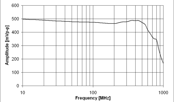
(click to enlarge)
Achievable performance
With the active input stage, much faster rise- and fall times can be achieved. Following picture shows a signal from a external clock having a fall time of about 300 ps being recorded with the AC-coupled version of the active input stage. The fall time of the recorded signal is about 800 ps, which is about the minimum which can be achieved with the AC-coupled version. The DC-coupled version achieves about 700ps.
|
Hi, stefan,
In the DC coupled version of the analog drivers for DRS4 input in Eval. Board V3, you mentioned that CMOFS of THS4508 was set to 1.8V to match the input range of DRS4, however, will this clash with the requirements of DRS4 input voltage between 0.1 V ~1.5V ? The output of THS4508 can easily rise beyond 1.5V for CMOFS=1.8V. I also noticed the resister paris R13/R15, R14/R16 was added among the output of THS4508 and the inputs of DRS4, were these resister pairs were used to attenuate the level of THS4508 output signal (a half ? ) to match the input requirements of DRS4? Maybe I have some misunderstanding about it.
|
|
107
|
Wed Jul 21 10:58:20 2010 |
Stefan Ritt | ENOB of DRS |
| Jinhong Wang wrote: |
|
Hi, Stefan, I see in your ppt "Design and performance of 6 GSPS waveform digitizing chip DRS4" , you define DRS4 ENOB as 1Vpp/0.35mv(RMS) = 11.5bit, where, 1Vpp is the linearity input range, and 0.35mv is the rms voltage after offset correction. What I understand is that 0.35mV is obtained from DC offset Correction, hence 11.5 bit is for DC input, am i right? If true, what about ENOB for AC input in the whole analog bandwidth? thanks~
|
The expression ENOB for 1Vpp/0.35mV(RMS) is wrong, but I learned this later. Now I call it SNR. The ENOB is calculated in a more complicated way, see for example http://en.wikipedia.org/wiki/ENOB. If you measure the ENOB without timing correction, it's pretty poor (in the order of 7-8 bits). This is because without timing calibration, a sine input has huge side bands, and the ENOB involves the power of your signal over the power of the side bands. If you do a proper timing calibration, you spectrum gets "sharper", and hence the ENOB increases. But I have to admit that I never measured it carefully, since we are still optimizing the timing calibration. Once we have a perfect timing calibration, I will do it and update the data sheet. |
|
106
|
Wed Jul 21 10:46:32 2010 |
Jinhong Wang | ENOB of DRS | Hi, Stefan, I see in your ppt "Design and performance of 6 GSPS waveform digitizing chip DRS4" , you define DRS4 ENOB as 1Vpp/0.35mv(RMS) = 11.5bit, where, 1Vpp is the linearity input range, and 0.35mv is the rms voltage after offset correction. What I understand is that 0.35mV is obtained from DC offset Correction, hence 11.5 bit is for DC input, am i right? If true, what about ENOB for AC input in the whole analog bandwidth? thanks~ |
|
105
|
Mon Jul 19 12:47:17 2010 |
Stefan Ritt | Fixed Patter Timing Jitter |
| Jinhong Wang wrote: |
|
Hi Stefan, can you give some suggestions on determination of fixed pattern timing jitter of DRS4? Thanks~
|
I will prepare some more detailed description of how to do this in the near future, but we are still learning ourselves constantly how to do that better.
So for the moment I only can recommend you to read the function DRSBoard::CalibrateTiming() and AnalyzeWF(). What you basically do is to define an array of "effective" bin widths t[i]. You start with the nominal bin width (let's say 500ps at 2 GSPS). Now you measure a periodic signal, and look for the zero crossings. If you have a 100 MHz clock, the time between two positive transitions (low-to-high) is 10.000ns. Now you measure the width as seen by the DRS chip, assuming the effective bin widths. The exact zero crossing you interpolate between two samples to improve the accuracy. Now you measure something different, let's say 10.1ns. So you know the ~20 bins between the zero crossings are "too wide", but you don't know which one of them is too wide. So you distribute the "too wide" equally between all bins, that is you decrease the effective width of these bins from 500ps to 500-0.1ns/20=499.995 ps. Then you do this iteratively, that is for all cycles in the waveform, and for many (1000's) of recorded waveforms. It is important that the phase of you measured clock is random, so that all bins are covered equally. Then you realize that the solution oscillates, which you can reduce by using a damping factor (called "damping" in my C code). So you do not correct to 499.995ps, but maybe to 499.999ps. If you iterate often enough, the solution kind of stabilizes.
The attached picture shows the result of such a calibration. Green is the effective bin width which in the end only slightly deviates from 500ps. But the "integral temporal nonlinearity" shows a typical shape for the DRS chip. It's defined as
n
Ti[n] = Sum (t[i]-500ps)
i=0
where t[i] is the effective bin width. So Ti[0] is zero by definition, but the deviation around bin 450 can go up to 1ns at 2 GSPS.
Now you can test you calibration, by measuring again the period of your clock. If you do everything correctly and have a low jitter external clock and no noise on your DRS4 power supply voltages, you should see a residual jitter of about 40ps.
Hope this explanation helps a bit. Let me know if I was not clear enough at some points.
- Stefan |
| Attachment 1: Capture.png
|

|
|
104
|
Mon Jul 19 12:07:04 2010 |
Jinhong Wang | Fixed Patter Timing Jitter | Hi Stefan, can you give some suggestions on determination of fixed pattern timing jitter of DRS4? Thanks~ |
|
99
|
Mon Jul 12 16:07:37 2010 |
Stefan Ritt | Announcement evaluation board V3 | Dear DRS4 users,
a new version of the evaluation board has been designed and is in production now. The main difference is that it uses active input amplifiers, which result in an analog bandwidth of 700 MHz (as compared with the 220 MHz of the previous board) at moderate power consumption, so the board can still be powered by the USB port. New orders will receive boards V3, the old V2 boards are not available any more.
It is mandatory to use the software revision 3.0.0 or later with the new board. This software has also many new features in the oscilloscope application, and together with the new firmware it reduces the noise of the board below 0.5 mV RMS. Although the software can be used with old V2 boards, some limitations might apply due to the old firmware of the boards. People having a Xilinx download cable can flash the firmware contained in the 3.0.0 revision to their V2 board to get all features of the new software.
The evaluation board manual V3 contains the new schematics of the analog inputs using the THS4508 differential amplifier, so people doing their own design can use this schematics as and example.
Best regards,
Stefan Ritt |
| Attachment 1: eval3.png
|

|
|
98
|
Tue Jun 22 11:37:42 2010 |
Jinhong Wang | Reset of DRS4 |
| Stefan Ritt wrote: |
|
| Jinhong Wang wrote: |
|
| Stefan Ritt wrote: |
|
| Jinhong Wang wrote: |
|
Hi Stefan,
I found DRS draw a lot of current when applied Reset after power on, and the PLL does not work properly. I believe there was something that I misunderstood. So, what will happen when Reset is applied more than once after power on? . Though the chip worked well without a Reset, i want to try to find out what was wrong, for a better understanding of DRS.
best regards!
Jinhong
|
Have you made sure that DENABLE and DWRITE stays low during the reset?
|
Yes, they are stay low until Reset goes high. the process is as following
Step1: Reset ='1', DEnable ='0', DWrite ='0', Reg_addr ="1111", Rsload='0', Srin ='0'
Step2: Reset='0', the others do not change, the low of the pulse is longer than 10 ns.
Step3: Reset='1', the others do not change, wait for some time
Step4: DEnable ='1' to start the domino.
|
Ok, then I have no idea. I never tried several reset pulses (actually this is not needed), so I have to reproduce the problem myself and investigate it. Actually in all my designs the reset input is just left open, since the internal initial reset is enough, so I have to modify my design first...
|
Ok ,thank you. |
|
97
|
Tue Jun 22 11:35:18 2010 |
Stefan Ritt | Reset of DRS4 |
| Jinhong Wang wrote: |
|
| Stefan Ritt wrote: |
|
| Jinhong Wang wrote: |
|
Hi Stefan,
I found DRS draw a lot of current when applied Reset after power on, and the PLL does not work properly. I believe there was something that I misunderstood. So, what will happen when Reset is applied more than once after power on? . Though the chip worked well without a Reset, i want to try to find out what was wrong, for a better understanding of DRS.
best regards!
Jinhong
|
Have you made sure that DENABLE and DWRITE stays low during the reset?
|
Yes, they are stay low until Reset goes high. the process is as following
Step1: Reset ='1', DEnable ='0', DWrite ='0', Reg_addr ="1111", Rsload='0', Srin ='0'
Step2: Reset='0', the others do not change, the low of the pulse is longer than 10 ns.
Step3: Reset='1', the others do not change, wait for some time
Step4: DEnable ='1' to start the domino.
|
Ok, then I have no idea. I never tried several reset pulses (actually this is not needed), so I have to reproduce the problem myself and investigate it. Actually in all my designs the reset input is just left open, since the internal initial reset is enough, so I have to modify my design first... |
|
96
|
Tue Jun 22 11:29:26 2010 |
Jinhong Wang | Reset of DRS4 |
| Stefan Ritt wrote: |
|
| Jinhong Wang wrote: |
|
Hi Stefan,
I found DRS draw a lot of current when applied Reset after power on, and the PLL does not work properly. I believe there was something that I misunderstood. So, what will happen when Reset is applied more than once after power on? . Though the chip worked well without a Reset, i want to try to find out what was wrong, for a better understanding of DRS.
best regards!
Jinhong
|
Have you made sure that DENABLE and DWRITE stays low during the reset?
|
Yes, they are stay low until Reset goes high. the process is as following
Step1: Reset ='1', DEnable ='0', DWrite ='0', Reg_addr ="1111", Rsload='0', Srin ='0'
Step2: Reset='0', the others do not change, the low of the pulse is longer than 10 ns.
Step3: Reset='1', the others do not change, wait for some time
Step4: DEnable ='1' to start the domino. |
|
95
|
Tue Jun 22 11:02:30 2010 |
Stefan Ritt | Reset of DRS4 |
| Jinhong Wang wrote: |
|
Hi Stefan,
I found DRS draw a lot of current when applied Reset after power on, and the PLL does not work properly. I believe there was something that I misunderstood. So, what will happen when Reset is applied more than once after power on? . Though the chip worked well without a Reset, i want to try to find out what was wrong, for a better understanding of DRS.
best regards!
Jinhong
|
Have you made sure that DENABLE and DWRITE stays low during the reset? |
|
94
|
Tue Jun 22 10:50:19 2010 |
Jinhong Wang | Reset of DRS4 | Hi Stefan,
I found DRS draw a lot of current when applied Reset after power on, and the PLL does not work properly. I believe there was something that I misunderstood. So, what will happen when Reset is applied more than once after power on? . Though the chip worked well without a Reset, i want to try to find out what was wrong, for a better understanding of DRS.
best regards!
Jinhong |
|
93
|
Sat Jun 19 10:09:18 2010 |
Jinhong Wang | DVDD Problem of DRS 4 |
| Stefan Ritt wrote: |
|
| Jinhong Wang wrote: |
|
Hi Stefan
I designed the evaluation board for our experiment. On our boards, I encountered the similar problem when working on the PLL of DRS4. I compared the following two configuration process, which on with PLL locked, the other not,
Process1:
step 1: Set DEnable and DWrite low,
Step2 : Reset DRS4 with a negative pulse of about 900 ns
Step3: Set DEnable high, thus do nothing but wait
I found DRS4 PLL working and locked.
Process 2:
Step 1: Set DEnable and DWrite low,
Step2 : Reset DRS4 with a negative pulse of about 900 ns
Step3: Set Config. Register( "11111111" .of course, this step was not necessary, just to see whether SPI was working properly from DTAP when set to "11111110")
Step4: Set The read shift Register ( full read out mode)
Step5: Set DEnable high,
Step6: Set DWrite high , thus low it , and prepare to read the waveform.
Well, I found in this case, the PLL was not locked, I am sure there was no problem with my SPI configuration process of DRS4.
toggle from DTAP could be viewed, but not stable.
Any Suggestions ?
thanks.
|
So the main difference, if I understand correctly, is the setting of the Config Register. Actually I never tried that, I always went with the default settings (all "1"). What happens if you write "00000000"? You know Bit1 controls the PLL, maybe there is a bug and the signal needs to be inverted.
|
Hi, Stefan,
The problem was fixed by setting Reg_addr "1001" instead of "1111" when in idle state, I was confused. |
|
92
|
Fri Jun 18 11:45:18 2010 |
Stefan Ritt | DVDD Problem of DRS 4 |
| Jinhong Wang wrote: |
|
Hi Stefan
I designed the evaluation board for our experiment. On our boards, I encountered the similar problem when working on the PLL of DRS4. I compared the following two configuration process, which on with PLL locked, the other not,
Process1:
step 1: Set DEnable and DWrite low,
Step2 : Reset DRS4 with a negative pulse of about 900 ns
Step3: Set DEnable high, thus do nothing but wait
I found DRS4 PLL working and locked.
Process 2:
Step 1: Set DEnable and DWrite low,
Step2 : Reset DRS4 with a negative pulse of about 900 ns
Step3: Set Config. Register( "11111111" .of course, this step was not necessary, just to see whether SPI was working properly from DTAP when set to "11111110")
Step4: Set The read shift Register ( full read out mode)
Step5: Set DEnable high,
Step6: Set DWrite high , thus low it , and prepare to read the waveform.
Well, I found in this case, the PLL was not locked, I am sure there was no problem with my SPI configuration process of DRS4.
toggle from DTAP could be viewed, but not stable.
Any Suggestions ?
thanks.
|
So the main difference, if I understand correctly, is the setting of the Config Register. Actually I never tried that, I always went with the default settings (all "1"). What happens if you write "00000000"? You know Bit1 controls the PLL, maybe there is a bug and the signal needs to be inverted. |
|
91
|
Fri Jun 18 11:31:20 2010 |
Jinhong Wang | DVDD Problem of DRS 4 |
| Stefan Ritt wrote: |
|
| Hao Huan wrote: |
|
| Stefan Ritt wrote: |
|
| Hao Huan wrote: |
|
| Stefan Ritt wrote: |
|
| Hao Huan wrote: |
|
Hi Stefan,
on our board some DRS chips draw a lot of current through DVDD after power-up and heat up significantly--it is true that our board doesn't have weak pull-down resistors at DENABLE and DWRITE output pins of FPGA, so this problem might have been caused by that, but a reinitialization of the Domino circuit doesn't help either. We tried different capacitors at DVDD and it seemed the larger the capacitance, the better the result--with a capacitor larger than 10nF some of the DRS chips could work happily in the normal way while if the capacitor is only 4.7nF all of them got very hot. Would you please provide some suggestions why there should be such a problem?
Thanks a lot!
|
I found that sometimes even a reinitialization fails if the pull-down resistors are missing. So instead playing with capacitors at DVDD, I would just solder two resistors on the board which should fix the problem completely.
|
Thanks! After adding pull-down resistors the voltages come back to normal.
However there is another weird problem that arises: a reset pulse seems unable to set the internal shift registers to default values. For example, after reset without addressing the Config Register the PLL will not try to lock with external reference clock. Even if I explicitly address the Config Register after reset and have the PLL locked, some channels of the chip will give null output during readout while other channels work normally. Could it be that some channels are not initiated properly with the Domino circuit?
|
Something is wrong. I have 800 chips, and they all start up fine. Check with your scope the RESET, DSPEED, DENABLE and DTAP signals. When RESET is applied, DSPEED should go to 2.5 V. When DENABLE goes high, the domino wave is started and you should see DTAP toggle. DSPEED is then lowered by the PLL until DTAP matches your external reference clock. I usually keep DENABLE high all the time after initialization, so the domino wave just continues running.
Another problem could however be the chip readout. If some channel gives null output, it could be that your readout has a problem. Do you use RSRLOAD to initialize the readout sequence?
|
Yes; I used RSRLOAD to trigger readout of all channels in parallel so the asymmetry between channels of the same chip is really a big puzzle. Also during reset DSPEED indeed goes to 2.5V, but after reset the PLL will not try to lock with the external reference clock and lower DSPEED. Instead the Domino circuit just oscillates at the highest frequency by itself.
A more confusing discovery is that the SRIN level before starting the Domino wave could affect the behavior of the PLL. I mean the level of SRIN when the chip is at A="1111" or "1010". Is SRIN supposed to influence the chip even in these standby or transparent modes?
|
Just some ideas:
- Is DENABLE really kept high all the time?
- Is DRESET only applied once during initialization, after that it should stay high
- Does REFCLK+/REFCLK- really toggle at the required sampling speed / 2048?
- Is the REFCLK really a good differential signal? Note that it must be biased properly since the DRS4 inputs are high impedance
- Is the Bit1 in the Config Register really at "1" to enable the PLL?
The only way the SRIN level could affect the PLL is if you address the Config Register (A="1100") and you clock in a few bits with SRCLK.
Have you thought about 'crazy' things such as:
- Defining the DRS4 chip wronly in your CAD software so that the pins are different from what you think?
- Some soldering problem of the DRS4 chips (we had this in the past) so that some pins are not connected at all and others have shorts
I guess you checked most of the things, so I'm just wildly guessing in order to stimulate some thoughts.
The ultimate check would be to get one of the evaluation boards (I sent a few to Jean-Francois Genat some time ago...) and compare the DRS4 signals pin by pin.
|
Hi Stefan
I designed the evaluation board for our experiment. On our boards, I encountered the similar problem when working on the PLL of DRS4. I compared the following two configuration process, which on with PLL locked, the other not,
Process1:
step 1: Set DEnable and DWrite low,
Step2 : Reset DRS4 with a negative pulse of about 900 ns
Step3: Set DEnable high, thus do nothing but wait
I found DRS4 PLL working and locked.
Process 2:
Step 1: Set DEnable and DWrite low,
Step2 : Reset DRS4 with a negative pulse of about 900 ns
Step3: Set Config. Register( "11111111" .of course, this step was not necessary, just to see whether SPI was working properly from DTAP when set to "11111110")
Step4: Set The read shift Register ( full read out mode)
Step5: Set DEnable high,
Step6: Set DWrite high , thus low it , and prepare to read the waveform.
Well, I found in this case, the PLL was not locked, I am sure there was no problem with my SPI configuration process of DRS4.
toggle from DTAP could be viewed, but not stable.
Any Suggestions ?
thanks. |
|
88
|
Tue Jun 1 13:36:18 2010 |
Stefan Ritt | High Frequency Input for DRS |
| Hao Huan wrote: |
|
Hi Stefan,
I read in the DRS datasheet that the bandwidth for the transparent mode OUT+ is only 200MHz which I think cannot be improved by any active input buffer; so if you want to operate the chip for really high frequency input, would it be better to feed on-board discriminators not from the output of DRS but from the input end?
Thanks!
|
First, the 200 MHz is not correct. Table 1 clearly states ANALOG OUTPUTS - Bandwidth (-3dB): 50 MHz. This is also shown in plot 11 (revision 0.9). But that does not necessarily mean that you have to drive your discriminators from the input of the DRS4 chip. If you use this for triggering, a 1-2 ns timing jitter does not matter, since stopping the domino wave anyhow has a 3-4 cell jitter. If you send a very fast signal though a 50 MHz low pass filter, the timing anyhow doe not change, only the slope of your signal gets lower, so you are more sensitive to noise, which in turn causes the 1-2 ns timing jitter. But I personally would not worry about that too much. Putting any signal splitting components in the input path would reduce the input bandwidth, which would be much more of an issue. |
|
87
|
Wed May 26 19:18:09 2010 |
Hao Huan | High Frequency Input for DRS | Hi Stefan,
I read in the DRS datasheet that the bandwidth for the transparent mode OUT+ is only 200MHz which I think cannot be improved by any active input buffer; so if you want to operate the chip for really high frequency input, would it be better to feed on-board discriminators not from the output of DRS but from the input end?
Thanks!
|
|
86
|
Wed May 19 09:16:02 2010 |
Stefan Ritt | DVDD Problem of DRS 4 |
| Hao Huan wrote: |
|
| Stefan Ritt wrote: |
|
| Hao Huan wrote: |
|
| Stefan Ritt wrote: |
|
| Hao Huan wrote: |
|
Hi Stefan,
on our board some DRS chips draw a lot of current through DVDD after power-up and heat up significantly--it is true that our board doesn't have weak pull-down resistors at DENABLE and DWRITE output pins of FPGA, so this problem might have been caused by that, but a reinitialization of the Domino circuit doesn't help either. We tried different capacitors at DVDD and it seemed the larger the capacitance, the better the result--with a capacitor larger than 10nF some of the DRS chips could work happily in the normal way while if the capacitor is only 4.7nF all of them got very hot. Would you please provide some suggestions why there should be such a problem?
Thanks a lot!
|
I found that sometimes even a reinitialization fails if the pull-down resistors are missing. So instead playing with capacitors at DVDD, I would just solder two resistors on the board which should fix the problem completely.
|
Thanks! After adding pull-down resistors the voltages come back to normal.
However there is another weird problem that arises: a reset pulse seems unable to set the internal shift registers to default values. For example, after reset without addressing the Config Register the PLL will not try to lock with external reference clock. Even if I explicitly address the Config Register after reset and have the PLL locked, some channels of the chip will give null output during readout while other channels work normally. Could it be that some channels are not initiated properly with the Domino circuit?
|
Something is wrong. I have 800 chips, and they all start up fine. Check with your scope the RESET, DSPEED, DENABLE and DTAP signals. When RESET is applied, DSPEED should go to 2.5 V. When DENABLE goes high, the domino wave is started and you should see DTAP toggle. DSPEED is then lowered by the PLL until DTAP matches your external reference clock. I usually keep DENABLE high all the time after initialization, so the domino wave just continues running.
Another problem could however be the chip readout. If some channel gives null output, it could be that your readout has a problem. Do you use RSRLOAD to initialize the readout sequence?
|
Yes; I used RSRLOAD to trigger readout of all channels in parallel so the asymmetry between channels of the same chip is really a big puzzle. Also during reset DSPEED indeed goes to 2.5V, but after reset the PLL will not try to lock with the external reference clock and lower DSPEED. Instead the Domino circuit just oscillates at the highest frequency by itself.
A more confusing discovery is that the SRIN level before starting the Domino wave could affect the behavior of the PLL. I mean the level of SRIN when the chip is at A="1111" or "1010". Is SRIN supposed to influence the chip even in these standby or transparent modes?
|
Just some ideas:
- Is DENABLE really kept high all the time?
- Is DRESET only applied once during initialization, after that it should stay high
- Does REFCLK+/REFCLK- really toggle at the required sampling speed / 2048?
- Is the REFCLK really a good differential signal? Note that it must be biased properly since the DRS4 inputs are high impedance
- Is the Bit1 in the Config Register really at "1" to enable the PLL?
The only way the SRIN level could affect the PLL is if you address the Config Register (A="1100") and you clock in a few bits with SRCLK.
Have you thought about 'crazy' things such as:
- Defining the DRS4 chip wronly in your CAD software so that the pins are different from what you think?
- Some soldering problem of the DRS4 chips (we had this in the past) so that some pins are not connected at all and others have shorts
I guess you checked most of the things, so I'm just wildly guessing in order to stimulate some thoughts.
The ultimate check would be to get one of the evaluation boards (I sent a few to Jean-Francois Genat some time ago...) and compare the DRS4 signals pin by pin. |
|
85
|
Wed May 19 02:24:12 2010 |
Hao Huan | DVDD Problem of DRS 4 |
| Stefan Ritt wrote: |
|
| Hao Huan wrote: |
|
| Stefan Ritt wrote: |
|
| Hao Huan wrote: |
|
Hi Stefan,
on our board some DRS chips draw a lot of current through DVDD after power-up and heat up significantly--it is true that our board doesn't have weak pull-down resistors at DENABLE and DWRITE output pins of FPGA, so this problem might have been caused by that, but a reinitialization of the Domino circuit doesn't help either. We tried different capacitors at DVDD and it seemed the larger the capacitance, the better the result--with a capacitor larger than 10nF some of the DRS chips could work happily in the normal way while if the capacitor is only 4.7nF all of them got very hot. Would you please provide some suggestions why there should be such a problem?
Thanks a lot!
|
I found that sometimes even a reinitialization fails if the pull-down resistors are missing. So instead playing with capacitors at DVDD, I would just solder two resistors on the board which should fix the problem completely.
|
Thanks! After adding pull-down resistors the voltages come back to normal.
However there is another weird problem that arises: a reset pulse seems unable to set the internal shift registers to default values. For example, after reset without addressing the Config Register the PLL will not try to lock with external reference clock. Even if I explicitly address the Config Register after reset and have the PLL locked, some channels of the chip will give null output during readout while other channels work normally. Could it be that some channels are not initiated properly with the Domino circuit?
|
Something is wrong. I have 800 chips, and they all start up fine. Check with your scope the RESET, DSPEED, DENABLE and DTAP signals. When RESET is applied, DSPEED should go to 2.5 V. When DENABLE goes high, the domino wave is started and you should see DTAP toggle. DSPEED is then lowered by the PLL until DTAP matches your external reference clock. I usually keep DENABLE high all the time after initialization, so the domino wave just continues running.
Another problem could however be the chip readout. If some channel gives null output, it could be that your readout has a problem. Do you use RSRLOAD to initialize the readout sequence?
|
Yes; I used RSRLOAD to trigger readout of all channels in parallel so the asymmetry between channels of the same chip is really a big puzzle. Also during reset DSPEED indeed goes to 2.5V, but after reset the PLL will not try to lock with the external reference clock and lower DSPEED. Instead the Domino circuit just oscillates at the highest frequency by itself.
A more confusing discovery is that the SRIN level before starting the Domino wave could affect the behavior of the PLL. I mean the level of SRIN when the chip is at A="1111" or "1010". Is SRIN supposed to influence the chip even in these standby or transparent modes? |
|
84
|
Tue May 18 09:24:02 2010 |
Stefan Ritt | Reference design for DRS4 active input buffer | The design of high frequency differential input stages with the DRS4 is a challenge, since the chip draws quite some current at the input (up to 1 mA at 5 GSPS), which must be sourced by the input buffer. A simple transformer as used in the DRS4 Evaluation Board 2.0 limits the bandwidth to 220 MHz. In meantime two active input stages have been worked out and successfully been tested, both utilizing the THS4508 differential amplifier. The first design is AC-coupled and uses less power, the second design is DC-coupled and uses more power with the benefit of delivering a higher bandwidth.
Both designs use a clamping diode at the input as a protection against high voltage spikes at the input. We used a RCLAMP0502B diode from SEMTECH, but any fast voltage suppressor diode will do the job.
The CMOFS input to the THS4508 set the common mode of the differential amplifier. In the AC version the level is set to mid-rail (2.5V), in the DC version it's set to 1.8V to match the input range of the DRS4.
The CAL+ and CAL- signals are used to bias the inputs to a well-defined DC level and can also be used to calibrate the chip. For bipolar inputs, they are both set to 0.8V. A positive 0.5V input pulse then drives DRS_IN+ to (0.8+0.25)V = 1.05V and DRS_IN- to (0.8-0.25)V = 0.55V. A negative 0.5V pulse then drives then DRS_IN+ to 0.55V and DRS_IN- to 1.05V. With ROFS=1.6V, the full dynamic range of the DRS4 is then used. Note that the THS4508 has a gain of 2, and the input has a -6dB voltage divider to compensate for that. To use other input ranges, such as -1V...0V, the CAL+ and CAL- signals can be adjusted accordingly. Note that the inputs of the DRS4 must always be between 0.1V and 1.5V.
AC-coupled version
(click to enlarge)
Power supply: +5 V 40 mA
Bandwidth (-3dB): 600 MHz
CMOFS: 2.5 V
Transfer function:
(click to enlarge)
The transfer function was measured by applying a fixed amplitude sine wave to the input, and measuring the peak-to-peak value of the read out waveform with the DRSOsc application.
DC-coupled Version
The DC-coupled version has a slightly higher power consumption since there is a constant current flowing through the output into the DRS4 chip. On the other hand, the bandwidth is a bit higher and the peaking around 400 MHz is a bit smaller. The input is still AC-coupled, so both positive and negative pulses can be accepted.
(click to enlarge)
Power supply: +5 V 115 mA
Bandwidth (-3dB): 800 MHz
CMOFS: 1.8 V
Transfer function:
(click to enlarge)
Achievable performance
With the active input stage, much faster rise- and fall times can be achieved. Following picture shows a signal from a external clock having a fall time of about 300 ps being recorded with the AC-coupled version of the active input stage. The fall time of the recorded signal is about 800 ps, which is about the minimum which can be achieved with the AC-coupled version. The DC-coupled version achieves about 700ps.
|
|
83
|
Tue May 18 08:23:07 2010 |
Stefan Ritt | DVDD Problem of DRS 4 |
| Hao Huan wrote: |
|
| Stefan Ritt wrote: |
|
| Hao Huan wrote: |
|
Hi Stefan,
on our board some DRS chips draw a lot of current through DVDD after power-up and heat up significantly--it is true that our board doesn't have weak pull-down resistors at DENABLE and DWRITE output pins of FPGA, so this problem might have been caused by that, but a reinitialization of the Domino circuit doesn't help either. We tried different capacitors at DVDD and it seemed the larger the capacitance, the better the result--with a capacitor larger than 10nF some of the DRS chips could work happily in the normal way while if the capacitor is only 4.7nF all of them got very hot. Would you please provide some suggestions why there should be such a problem?
Thanks a lot!
|
I found that sometimes even a reinitialization fails if the pull-down resistors are missing. So instead playing with capacitors at DVDD, I would just solder two resistors on the board which should fix the problem completely.
|
Thanks! After adding pull-down resistors the voltages come back to normal.
However there is another weird problem that arises: a reset pulse seems unable to set the internal shift registers to default values. For example, after reset without addressing the Config Register the PLL will not try to lock with external reference clock. Even if I explicitly address the Config Register after reset and have the PLL locked, some channels of the chip will give null output during readout while other channels work normally. Could it be that some channels are not initiated properly with the Domino circuit?
|
Something is wrong. I have 800 chips, and they all start up fine. Check with your scope the RESET, DSPEED, DENABLE and DTAP signals. When RESET is applied, DSPEED should go to 2.5 V. When DENABLE goes high, the domino wave is started and you should see DTAP toggle. DSPEED is then lowered by the PLL until DTAP matches your external reference clock. I usually keep DENABLE high all the time after initialization, so the domino wave just continues running.
Another problem could however be the chip readout. If some channel gives null output, it could be that your readout has a problem. Do you use RSRLOAD to initialize the readout sequence? |
|
82
|
Tue May 18 01:47:59 2010 |
Hao Huan | DVDD Problem of DRS 4 |
| Stefan Ritt wrote: |
|
| Hao Huan wrote: |
|
Hi Stefan,
on our board some DRS chips draw a lot of current through DVDD after power-up and heat up significantly--it is true that our board doesn't have weak pull-down resistors at DENABLE and DWRITE output pins of FPGA, so this problem might have been caused by that, but a reinitialization of the Domino circuit doesn't help either. We tried different capacitors at DVDD and it seemed the larger the capacitance, the better the result--with a capacitor larger than 10nF some of the DRS chips could work happily in the normal way while if the capacitor is only 4.7nF all of them got very hot. Would you please provide some suggestions why there should be such a problem?
Thanks a lot!
|
I found that sometimes even a reinitialization fails if the pull-down resistors are missing. So instead playing with capacitors at DVDD, I would just solder two resistors on the board which should fix the problem completely.
|
Thanks! After adding pull-down resistors the voltages come back to normal.
However there is another weird problem that arises: a reset pulse seems unable to set the internal shift registers to default values. For example, after reset without addressing the Config Register the PLL will not try to lock with external reference clock. Even if I explicitly address the Config Register after reset and have the PLL locked, some channels of the chip will give null output during readout while other channels work normally. Could it be that some channels are not initiated properly with the Domino circuit? |
|
81
|
Fri May 14 08:40:14 2010 |
Stefan Ritt | DVDD Problem of DRS 4 |
| Hao Huan wrote: |
|
Hi Stefan,
on our board some DRS chips draw a lot of current through DVDD after power-up and heat up significantly--it is true that our board doesn't have weak pull-down resistors at DENABLE and DWRITE output pins of FPGA, so this problem might have been caused by that, but a reinitialization of the Domino circuit doesn't help either. We tried different capacitors at DVDD and it seemed the larger the capacitance, the better the result--with a capacitor larger than 10nF some of the DRS chips could work happily in the normal way while if the capacitor is only 4.7nF all of them got very hot. Would you please provide some suggestions why there should be such a problem?
Thanks a lot!
|
I found that sometimes even a reinitialization fails if the pull-down resistors are missing. So instead playing with capacitors at DVDD, I would just solder two resistors on the board which should fix the problem completely. |
|
80
|
Thu May 13 19:14:27 2010 |
Hao Huan | DVDD Problem of DRS 4 | Hi Stefan,
on our board some DRS chips draw a lot of current through DVDD after power-up and heat up significantly--it is true that our board doesn't have weak pull-down resistors at DENABLE and DWRITE output pins of FPGA, so this problem might have been caused by that, but a reinitialization of the Domino circuit doesn't help either. We tried different capacitors at DVDD and it seemed the larger the capacitance, the better the result--with a capacitor larger than 10nF some of the DRS chips could work happily in the normal way while if the capacitor is only 4.7nF all of them got very hot. Would you please provide some suggestions why there should be such a problem?
Thanks a lot! |
|
79
|
Wed May 12 16:26:12 2010 |
Stefan Ritt | DRS4 chip model |
| Jinhong Wang wrote: |
|
| Stefan Ritt wrote: |
|
| Ignacio Diéguez Estremera wrote: |
|
So i guess i won't be able to include drs4 in my simulations :-(. Any other suggestions? Maybe the S-params model you where working on? Anything is better than nothing :-)
|
Please find attached the S-parameters.
|
Hi, we plan to do a time interpolating among the eight channels on a single chip to obtain a maximum 40 GSPS (or, maybe 30 GSPS ) sampling rate. Hence RF behavior of the anlog input is very important for us.
Will you give us some advice on the modeling of the anlog input circuit of the chip? Perhaps just the Spice model of the analog input?
The attached S parameters I found here is for fs =1 GSPS, what about fs=5GSPS?
thanks in advance,
Jinhong Wang (wangjinh@mail.ustc.edu.cn ; alleyor.wang@gmail.com)
|
To be honest, we never really succeeded to do any good simulation above let's say 500 MHz. We carefully tried to simulate the bond wire of the chip, the parasitic capacitances of the traces of the chip etc. but we always were off by a factor or two or so. Other groups reported the same problems. Some even did some 3D simulation model, without success. So our conclusion is that if you are interested in anything precise above 500 MHz, do a measurement.
So our current best design is with the THS4508. There is an AC coupled version going to 600 MHz, and a DC coupled version (uses more power) going to 800 MHz (-3dB). If you use passive inputs with a transformer for example, you can't go above 220 MHz. Next week I will publish both designs in this forum. |
|
78
|
Wed May 12 11:47:39 2010 |
Jinhong Wang | DRS4 chip model |
| Stefan Ritt wrote: |
|
| Ignacio Diéguez Estremera wrote: |
|
So i guess i won't be able to include drs4 in my simulations :-(. Any other suggestions? Maybe the S-params model you where working on? Anything is better than nothing :-)
|
Please find attached the S-parameters.
|
Hi, we plan to do a time interpolating among the eight channels on a single chip to obtain a maximum 40 GSPS (or, maybe 30 GSPS ) sampling rate. Hence RF behavior of the anlog input is very important for us.
Will you give us some advice on the modeling of the anlog input circuit of the chip? Perhaps just the Spice model of the analog input?
The attached S parameters I found here is for fs =1 GSPS, what about fs=5GSPS?
thanks in advance,
Jinhong Wang (wangjinh@mail.ustc.edu.cn ; alleyor.wang@gmail.com) |
|
77
|
Thu May 6 08:15:39 2010 |
Stefan Ritt | Random noise spec in datasheet |
| Ignacio Diéguez Estremera wrote: |
|
Hi,
According to DRS4's datasheet, the random noise is 0.35mVrms. Is this the input equivalent noise voltage? It is computed over the 0-950MHz frequency band?
Regards.
|
You cannot compare the DRS4 noise directly with an amplifier for example. The noise mainly comes from variations of the charge injection into the storage cells, and some noise during the readout process, which happens in a completely different frequency domain than the sampling.
So what I did is to keep the inputs open, measure a 1024-bin waveform, and compute the RMS of this waveform. So I believe that this is kind of equivalent noise voltage from 1-950 MHz. It does not start from zero since very low frequency noise (like 50 Hz) just causes a baseline shift and does not influence the RMS, but this is not so important since in most applications people do an event-by-event baseline subtraction to get rid of low frequency noise in their apparatus. The 0.35 mV RMS also depend on the electronics around the chip. On our USB evaluation board the noise it typically smaller (0.31 mV RMS), while in some VME board we measure 0.42 mV RMS. If you do the perfect analog design around the chip, you can maybe push this maybe even lower. |
|
76
|
Wed May 5 22:30:50 2010 |
Ignacio Di�guez Estremera | Random noise spec in datasheet | Hi,
According to DRS4's datasheet, the random noise is 0.35mVrms. Is this the input equivalent noise voltage? It is computed over the 0-950MHz frequency band?
Regards. |
|
75
|
Tue May 4 16:23:16 2010 |
Ignacio Di�guez Estremera | DRS4 chip model |
| Stefan Ritt wrote: |
|
| Ignacio Diéguez Estremera wrote: |
|
So i guess i won't be able to include drs4 in my simulations :-(. Any other suggestions? Maybe the S-params model you where working on? Anything is better than nothing :-)
|
Please find attached the S-parameters.
|
Thanks :-) |
|
74
|
Tue May 4 11:26:21 2010 |
Stefan Ritt | DRS4 chip model |
| Ignacio Diéguez Estremera wrote: |
|
So i guess i won't be able to include drs4 in my simulations :-(. Any other suggestions? Maybe the S-params model you where working on? Anything is better than nothing :-)
|
Please find attached the S-parameters. |
| Attachment 1: DRS4_S-Parameter.pdf
|


|
|
73
|
Mon May 3 23:21:55 2010 |
Ignacio Di�guez Estremera | DRS4 chip model |
| Stefan Ritt wrote: |
|
| Ignacio Diéguez Estremera wrote: |
|
| Stefan Ritt wrote: |
|
| Ignacio Diéguez Estremera wrote: |
|
Hi all,
i'm an electronics engineering student at UCM (Madrid) working on my master's thesis within the CTA collaboration. I'm designing the readout electronics for the telescope's camera, and i'm focusing in using GAPDs instead of PMTs and using the domino chip for the sampling of the signal. I was wondering if there is a spice and/or RF model of the DRS4 chip available. It would be very useful to perform some simulations before deciding to use the chip as the sampling solution for our prototypes.
If the answer is negative, can you give me some advise for modelling the chip in spice? Have you done any simulations?
Thanks in advance,
Ignacio Diéguez Estremera.
|
Yes there is a transistor-level spice model, which I used to design the chip, but you won't be happy with it: Given the 500,000+ transistors on the chip, a 100 ns simulation takes a couple of weeks. We tried to make a simplified model just for the analog input using some measured S-parameters, but found that the RF behavior of the chip is almost impossible to describe to better than let's say 50%. In the end you have to fine-tune your analog front-end experimentally, to obtain optimal bandwidth. We are just working on a reference design with gives you 850 MHz bandwidth using an active input buffer.
|
Thanks for the information.
I would like to try the huge :-) model. Can you send it to my email address? Since the input signal are pulses of a few nanoseconds at FHWM, the simulation time may be reduced. I will post some feedback in the forum once i give it a try.
Kind regards.
|
I just checked and realized that we are not allowed to give out the "huge" model since it contains parameters from the chip manufacturer's library which are confidentially.
|
Thank you for the effort anyway.
So i guess i won't be able to include drs4 in my simulations :-(. Any other suggestions? Maybe the S-params model you where working on? Anything is better than nothing :-) |
|
72
|
Mon May 3 17:10:29 2010 |
Stefan Ritt | DRS4 chip model |
| Ignacio Diéguez Estremera wrote: |
|
| Stefan Ritt wrote: |
|
| Ignacio Diéguez Estremera wrote: |
|
Hi all,
i'm an electronics engineering student at UCM (Madrid) working on my master's thesis within the CTA collaboration. I'm designing the readout electronics for the telescope's camera, and i'm focusing in using GAPDs instead of PMTs and using the domino chip for the sampling of the signal. I was wondering if there is a spice and/or RF model of the DRS4 chip available. It would be very useful to perform some simulations before deciding to use the chip as the sampling solution for our prototypes.
If the answer is negative, can you give me some advise for modelling the chip in spice? Have you done any simulations?
Thanks in advance,
Ignacio Diéguez Estremera.
|
Yes there is a transistor-level spice model, which I used to design the chip, but you won't be happy with it: Given the 500,000+ transistors on the chip, a 100 ns simulation takes a couple of weeks. We tried to make a simplified model just for the analog input using some measured S-parameters, but found that the RF behavior of the chip is almost impossible to describe to better than let's say 50%. In the end you have to fine-tune your analog front-end experimentally, to obtain optimal bandwidth. We are just working on a reference design with gives you 850 MHz bandwidth using an active input buffer.
|
Thanks for the information.
I would like to try the huge :-) model. Can you send it to my email address? Since the input signal are pulses of a few nanoseconds at FHWM, the simulation time may be reduced. I will post some feedback in the forum once i give it a try.
Kind regards.
|
I just checked and realized that we are not allowed to give out the "huge" model since it contains parameters from the chip manufacturer's library which are confidentially. |
|
71
|
Mon May 3 17:06:02 2010 |
Ignacio Di�guez Estremera | DRS4 chip model |
| Stefan Ritt wrote: |
|
| Ignacio Diéguez Estremera wrote: |
|
Hi all,
i'm an electronics engineering student at UCM (Madrid) working on my master's thesis within the CTA collaboration. I'm designing the readout electronics for the telescope's camera, and i'm focusing in using GAPDs instead of PMTs and using the domino chip for the sampling of the signal. I was wondering if there is a spice and/or RF model of the DRS4 chip available. It would be very useful to perform some simulations before deciding to use the chip as the sampling solution for our prototypes.
If the answer is negative, can you give me some advise for modelling the chip in spice? Have you done any simulations?
Thanks in advance,
Ignacio Diéguez Estremera.
|
Yes there is a transistor-level spice model, which I used to design the chip, but you won't be happy with it: Given the 500,000+ transistors on the chip, a 100 ns simulation takes a couple of weeks. We tried to make a simplified model just for the analog input using some measured S-parameters, but found that the RF behavior of the chip is almost impossible to describe to better than let's say 50%. In the end you have to fine-tune your analog front-end experimentally, to obtain optimal bandwidth. We are just working on a reference design with gives you 850 MHz bandwidth using an active input buffer.
|
Thanks for the information.
I would like to try the huge :-) model. Can you send it to my email address? Since the input signal are pulses of a few nanoseconds at FHWM, the simulation time may be reduced. I will post some feedback in the forum once i give it a try.
Kind regards. |
|
70
|
Mon May 3 11:09:12 2010 |
Stefan Ritt | DRS4 chip model |
| Ignacio Diéguez Estremera wrote: |
|
Hi all,
i'm an electronics engineering student at UCM (Madrid) working on my master's thesis within the CTA collaboration. I'm designing the readout electronics for the telescope's camera, and i'm focusing in using GAPDs instead of PMTs and using the domino chip for the sampling of the signal. I was wondering if there is a spice and/or RF model of the DRS4 chip available. It would be very useful to perform some simulations before deciding to use the chip as the sampling solution for our prototypes.
If the answer is negative, can you give me some advise for modelling the chip in spice? Have you done any simulations?
Thanks in advance,
Ignacio Diéguez Estremera.
|
Yes there is a transistor-level spice model, which I used to design the chip, but you won't be happy with it: Given the 500,000+ transistors on the chip, a 100 ns simulation takes a couple of weeks. We tried to make a simplified model just for the analog input using some measured S-parameters, but found that the RF behavior of the chip is almost impossible to describe to better than let's say 50%. In the end you have to fine-tune your analog front-end experimentally, to obtain optimal bandwidth. We are just working on a reference design with gives you 850 MHz bandwidth using an active input buffer. |
|
69
|
Sun May 2 18:36:14 2010 |
Ignacio Di�guez Estremera | DRS4 chip model | Hi all,
i'm an electronics engineering student at UCM (Madrid) working on my master's thesis within the CTA collaboration. I'm designing the readout electronics for the telescope's camera, and i'm focusing in using GAPDs instead of PMTs and using the domino chip for the sampling of the signal. I was wondering if there is a spice and/or RF model of the DRS4 chip available. It would be very useful to perform some simulations before deciding to use the chip as the sampling solution for our prototypes.
If the answer is negative, can you give me some advise for modelling the chip in spice? Have you done any simulations?
Thanks in advance,
Ignacio Diéguez Estremera. |
|
68
|
Thu Apr 15 13:48:40 2010 |
Stefan Ritt | ROFS Configuration |
| Hao Huan wrote: |
|
Hi Stefan,
according to the DRS4 datasheet, if we want an input range centered around U0, the ROFS should be 1.55V-U0. However when I read the codes of the evaluation board application, ROFS seems to be 1.6V-1.25*U0 where the coefficient 1.25 is said to come from sampling cell charge injection correction. Is it the right equation to use? What exactly does that charge injection correction mean?
Thanks a lot.
|
1.55V-U0 is the theoretical values, but there are certain "dirt" effects like chip-to-chip variation and charge injection. The difference between various chips is easily 20-30mV, so there is not a single "correct" value. The formula 1.6V-1.25*U0 I developed for a special evaluation board, where it kind of worked better than the theoretical value, but I never made systematic studies. One should average over several chips and use some solid average there. Best is if you try both formulas and check what give you the better linearity. |
|
67
|
Wed Apr 14 16:34:28 2010 |
Stefan Ritt | version 1.2 evaluation board with firmware 13279? |
| Heejong Kim wrote: |
Hi, Stefan,

I found that my collaborator bought 2 older version of evaluation board before.
They are the version 1.2 in plastics case with firmware 13191.

Can I upgrade the firmware from 13191 to 13279?
I'm wondering if the older version of evaluation board is working with firmware 13279.

Thanks,
Heejong
|
I checked and there is no significant difference between the two revisions, so I would just leave it. |
|
66
|
Tue Apr 13 14:15:16 2010 |
Stefan Ritt | Simple example application to read a DRS evaluation board |
| Heejong Kim wrote: |
|
| Stefan Ritt wrote: |
|
Several people asked for s simple application to guide them in writing their own application to read out a DRS board. Such an application has been added in software revions 2.1.1 and is attached to this message. This example program drs_exam.cpp written in C++ does the following necessary steps to access a DRS board:
- Crate a "DRS" object and scan all USB devices
- Display found DRS boards
- Initialize the first found board and set the sampling frequency to 5 GSPS
- Enable internal trigger on channel #1 with 250 mV threshold
- Start acquisition and wait for a trigger
- Read two waveforms (both time and amplitude)
- Repeat this 10 times
I know that we are still missing a good documentation for the DRS API, but I have not yet found the time to do that. I hope the example program is enough for most people to start writing own programs. For Windows users (MS Visual C++ 8.0) there is a drs.sln project file, and for linux users there is a Makefile which can be used to compile this example program.
|
Hi, Stefan,
drs_exam.cpp is working good to read-out one board.
Now I would like to read-out two boards at the same time using the same trigger( external or internal).
I'm trying to understand and modify the original code for control two board.
Meantime, it would be very appreciated if you give any tips for this.
Thanks,
Heejong
|
The evaluation boards are not really made for multi-board applications. What you have to do is to maintain an external trigger which synchronizes the boards. So you need:
- two boards connected to two USB ports
- an external flip-flop connected to the two trigger inputs of both boards
If a trigger is sent to the flip-flop, it sends a trigger to both evaluation boards. You poll on one of the boards to see if it has triggered (vis IsBusy()), then you read out both boards. Now you have to reset the external flip-flop somehow from the computer. If you have a CAMAC I/O board or some other means of sending a logical signal to it, that could do the job. From the software point, you get a "DRS" object upon initialization, which contains then two "DRSBoard" objects, over which you can iterate. Look at the "drscl" program from the distribution on how to do that. |
|
65
|
Tue Apr 13 13:56:07 2010 |
Stefan Ritt | Baseline Variation In Data |
| Hao Huan wrote: |
|
Hi Stefan,
when I sample a constant input with the DRS 4 chip, there was a baseline variation showing up as a saw-tooth pattern which grows with the absolute value of the differential input. Do you think this is the kind of baseline variation mentioned in the evaluation board manual, i.e. coming from clock jitter in ADC sampling?
Thanks a lot!
|
Please post an oscilloscope screenshot here and I can tell you. |
|
64
|
Tue Apr 13 13:12:43 2010 |
Stefan Ritt | evaluation board used like a counter |
| lorenzo neri wrote: |
|
Hi all
it is possible to use the evaluation board like a counter?
I'm interested in the arriving time of all self trigger event in to a channel.
the input signal are 2V TTL of 10 ns at 50ohm, and the time acquisition window is 1 second.
|
The evaluation board is as good or bad as an digital oscilloscope to work like a counter. At 1 GSPS, you have a window of one microsecond, which is certainly too short for your application. |
|
63
|
Tue Apr 13 10:45:18 2010 |
lorenzo neri | evaluation board used like a counter | Hi all
it is possible to use the evaluation board like a counter?
I'm interested in the arriving time of all self trigger event in to a channel.
the input signal are 2V TTL of 10 ns at 50ohm, and the time acquisition window is 1 second.
can someone help me?
thanks in advance,
Lorenzo |
|
62
|
Fri Apr 9 17:14:45 2010 |
Hao Huan | Baseline Variation In Data | Hi Stefan,
when I sample a constant input with the DRS 4 chip, there was a baseline variation showing up as a saw-tooth pattern which grows with the absolute value of the differential input. Do you think this is the kind of baseline variation mentioned in the evaluation board manual, i.e. coming from clock jitter in ADC sampling?
Thanks a lot!
|
|
61
|
Mon Apr 5 17:57:41 2010 |
Heejong Kim | Simple example application to read a DRS evaluation board |
| Stefan Ritt wrote: |
|
Several people asked for s simple application to guide them in writing their own application to read out a DRS board. Such an application has been added in software revions 2.1.1 and is attached to this message. This example program drs_exam.cpp written in C++ does the following necessary steps to access a DRS board:
- Crate a "DRS" object and scan all USB devices
- Display found DRS boards
- Initialize the first found board and set the sampling frequency to 5 GSPS
- Enable internal trigger on channel #1 with 250 mV threshold
- Start acquisition and wait for a trigger
- Read two waveforms (both time and amplitude)
- Repeat this 10 times
I know that we are still missing a good documentation for the DRS API, but I have not yet found the time to do that. I hope the example program is enough for most people to start writing own programs. For Windows users (MS Visual C++ 8.0) there is a drs.sln project file, and for linux users there is a Makefile which can be used to compile this example program.
|
Hi, Stefan,
drs_exam.cpp is working good to read-out one board.
Now I would like to read-out two boards at the same time using the same trigger( external or internal).
I'm trying to understand and modify the original code for control two board.
Meantime, it would be very appreciated if you give any tips for this.
Thanks,
Heejong |
|
60
|
Mon Apr 5 17:50:39 2010 |
Heejong Kim | version 1.2 evaluation board with firmware 13279? |
Hi, Stefan,

I found that my collaborator bought 2 older version of evaluation board before.
They are the version 1.2 in plastics case with firmware 13191.

Can I upgrade the firmware from 13191 to 13279?
I'm wondering if the older version of evaluation board is working with firmware 13279.

Thanks,
Heejong
|
|
59
|
Tue Mar 30 22:57:34 2010 |
Hao Huan | ROFS Configuration | Hi Stefan,
according to the DRS4 datasheet, if we want an input range centered around U0, the ROFS should be 1.55V-U0. However when I read the codes of the evaluation board application, ROFS seems to be 1.6V-1.25*U0 where the coefficient 1.25 is said to come from sampling cell charge injection correction. Is it the right equation to use? What exactly does that charge injection correction mean?
Thanks a lot.
|
|
58
|
Mon Mar 22 09:12:19 2010 |
Stefan Ritt | PLL Loop Filter Configuration |
| Hao Huan wrote: |
|
in the datasheet it says at 6GSPS the typical loop filter parameters are 220Ω, 2.2nF and 27nF. If I want to run the Domino wave nominally at 1GHz, i.e. with a reference clock frequency around 0.5MHz, is there any recommended loop filter configuration? Is the setup of the evaluation board, that is, 220Ω, 3.3nF and 33nF an optimal choice?
|
The setup of the evaluation board is a good compromise which runs between 1 GHz and 5 GHz. Unfortunately I never found the time to investigate this in more detail. So if someone is willing to measure settling time and phase jitter with various combinations of R, C1 and C2, I'm more than happy to include this into the datasheet. |
|
57
|
Sun Mar 21 02:03:44 2010 |
Hao Huan | PLL Loop Filter Configuration | Hi Stefan,
in the datasheet it says at 6GSPS the typical loop filter parameters are 220Ω, 2.2nF and 27nF. If I want to run the Domino wave nominally at 1GHz, i.e. with a reference clock frequency around 0.5MHz, is there any recommended loop filter configuration? Is the setup of the evaluation board, that is, 220Ω, 3.3nF and 33nF an optimal choice?
Thank you very much.
|
|
56
|
Thu Mar 18 22:10:41 2010 |
Stefan Ritt | Serial Interface Frequency of the DRS Chip |
| Hao Huan wrote: |
|
Thanks! The suggested algorithm looks promising. However, if the spikes take place only for those specific cells, is it possible to absorb them into the offset calibration?
|
No, since they are not constant. The bus segments charge up between readouts with a time constant of about 0.5s. So if you do the readout with 1Hz event rate and with 100Hz event rate, the peaks will differ by a factor up to 10, so a constant offset correction cannot take care of that. |
|
55
|
Thu Mar 18 21:38:10 2010 |
Hao Huan | Serial Interface Frequency of the DRS Chip |
| Stefan Ritt wrote: |
|
| Hao Huan wrote: |
|
in the DRS4 datasheet I read that the optimal frequency for SRCLK is 33MHz. However in the evaluation board firmware SRCLK is toggled at rising edges of the internal 33MHz clock, i.e. the frequency of SRCLK itself is 16.5MHz instead. Is that frequency better than 33MHz?
|
The reason for the 16.5 MHz is the following:
After each block of 32 bins, the DRS4 chip switches an internal segment, which causes some small spike at the analog output of the chip. This spike is a bit wider than 30ns, so if everything is digitized with 33 MHz, then you see small spiked each 32 cells. The appropriate solution would be to modify the firmware to digitize all cells with 30ns (33 MHz) and all cells with the spike with ~50 ns (20 MHz). If you do the ROI readout mode, you don't know for the first 10 cells if one of them belong to this class, since the cell address takes 10 cycles to be read out. So you would first have to read 10 cells, and then if you realize that one of them is one of the problematic ones (cell number modulo 32 is zero), you have to re-read the first 10 cells, and digitize the problematic cell with a longer settling time. Now this is a bit complicated to implement in the firmware, so I was just too lazy to do it and decided to digitize everything with 16.5 MHz. But if you are worried about the dead time, you should consider implementing the mentioned algorithm.
|
Thanks! The suggested algorithm looks promising. However, if the spikes take place only for those specific cells, is it possible to absorb them into the offset calibration? |
|
54
|
Fri Mar 12 08:04:44 2010 |
Stefan Ritt | Input Bandwidth of the DRS Chip |
| Hao Huan wrote: |
|
I read in the DRS datasheet that the input bandwidth if 950MHz. However, it also says the output bandwidth in the transparent mode is 50MHz. Since in the transparent mode the input is routed to the output, does it mean the input bandwidth also gets reduced in the transparent mode? I don't know how the transparent mode works inside the chip of course, but this value would be important since if the hardware discriminators are connected to the output of DRS, we have to always work in the transparent mode.
|
In transparent mode, the input signal also gets routed to the output, where it goes through an output buffer, which limits the bandwidth to about 50 MHz, but only for the output. The effective bandwidth to the sampling cells is not changed. Please note however that the 950 MHz are for the "chip only". We measured this by keeping the input amplitude from a function generator constant at the input pin of the chip (measured with a high speed oscilloscope). Since each signal source has a non-zero impedance, the signal tends to "shrink" at high bandwidth, and we had to adjust the level of the function generator to keep the amplitude constant at high frequencies. If you do a realistic input stage with the THS4508 for example, the achievable bandwidth will be around 800 MHz. |
|
53
|
Thu Mar 11 21:37:32 2010 |
Hao Huan | Input Bandwidth of the DRS Chip | Hi Stefan,
I read in the DRS datasheet that the input bandwidth if 950MHz. However, it also says the output bandwidth in the transparent mode is 50MHz. Since in the transparent mode the input is routed to the output, does it mean the input bandwidth also gets reduced in the transparent mode? I don't know how the transparent mode works inside the chip of course, but this value would be important since if the hardware discriminators are connected to the output of DRS, we have to always work in the transparent mode.
Thanks!
|
|
52
|
Thu Mar 11 11:45:52 2010 |
Stefan Ritt | Readout of DRS Data |
| Hao Huan wrote: |
|
Hi Stefan,
thanks to your help I can now successfully keep the Domino wave running at a stable frequency and maintain the channel cascading information in the Write Shift Register. (Since you told me WSR always reads and writes at the same time, I think I need to rewrite the information back every time after reading out from WSR to decide from which channel my data come, don't I?)
|
Yes you do. But if you have WSRLOOP=1 in the config register, this is done automatically. So the SR output is visible at the pin and will be fed back into the input.
| Hao Huan wrote: |
|
However I'm still having difficulty in reading out from the DRS cells. I use the ROI readout mode and assume as long as I give a pulse on RSRLOAD the data will come out one by one.
|
That's not correct. Have a look at Figure 14 of the datasheet. Do you see a single RSRLOAD pulse or many? There is only one RSRLOAD pulse to initialize the readout shift register, then the cells are clocked by SRCLK pulses.
| Hao Huan wrote: |
|
Also I read in the datasheet that WSROUT will give RSR output when DWRITE is low. Sometimes I see some random bits from this output and sometimes I see all zero's. What is the reasonable output I should see from WSROUT, say, when I'm running in the transparent mode with DWRITE low?
|
A single RSRLOAD pulse loads the RSR with a "1" at the domino stop position and "0" in all other places. A pulse on SRCLK shifts this "1" down the RSR. When it arrives at cell #1023, it will be visible for one clock cycle at WSROUT. The "double" functionality of WSROUT has the following background: Assume you use channel cascading 2x2048. Now the domino wave stopps in cell 1020 of the first channel for example. You have to read cells 1020,1021,1022,1024 of the first channel, then you continue with 0,1,2 on the second channel. But how do you know that you have to switch channels after the first four clock cycles? The SROUT output encodes the stop position (in this case 1020), but it needs 10 clock cycles before the information is available, so you don't have it after four cycles. That's where WSROUT comes into play: Since it outputs RSR bit by bit, it will show three "0", then a "1", when you are at cell 1023. Then you know that you have to switch channels immediately. That's why I output RSR via WSROUT if DWRITE is low.
|
|
51
|
Wed Mar 10 10:07:28 2010 |
Stefan Ritt | Serial Interface Frequency of the DRS Chip |
| Hao Huan wrote: |
|
in the DRS4 datasheet I read that the optimal frequency for SRCLK is 33MHz. However in the evaluation board firmware SRCLK is toggled at rising edges of the internal 33MHz clock, i.e. the frequency of SRCLK itself is 16.5MHz instead. Is that frequency better than 33MHz?
|
The reason for the 16.5 MHz is the following:
After each block of 32 bins, the DRS4 chip switches an internal segment, which causes some small spike at the analog output of the chip. This spike is a bit wider than 30ns, so if everything is digitized with 33 MHz, then you see small spiked each 32 cells. The appropriate solution would be to modify the firmware to digitize all cells with 30ns (33 MHz) and all cells with the spike with ~50 ns (20 MHz). If you do the ROI readout mode, you don't know for the first 10 cells if one of them belong to this class, since the cell address takes 10 cycles to be read out. So you would first have to read 10 cells, and then if you realize that one of them is one of the problematic ones (cell number modulo 32 is zero), you have to re-read the first 10 cells, and digitize the problematic cell with a longer settling time. Now this is a bit complicated to implement in the firmware, so I was just too lazy to do it and decided to digitize everything with 16.5 MHz. But if you are worried about the dead time, you should consider implementing the mentioned algorithm. |
|
50
|
Tue Mar 9 23:28:45 2010 |
Hao Huan | Serial Interface Frequency of the DRS Chip | Hi Stefan,
in the DRS4 datasheet I read that the optimal frequency for SRCLK is 33MHz. However in the evaluation board firmware SRCLK is toggled at rising edges of the internal 33MHz clock, i.e. the frequency of SRCLK itself is 16.5MHz instead. Is that frequency better than 33MHz?
Thanks!
|
|
49
|
Fri Mar 5 23:29:04 2010 |
Hao Huan | Readout of DRS Data |
| Hao Huan wrote: |
|
Hi Stefan,
thanks to your help I can now successfully keep the Domino wave running at a stable frequency and maintain the channel cascading information in the Write Shift Register. (Since you told me WSR always reads and writes at the same time, I think I need to rewrite the information back every time after reading out from WSR to decide from which channel my data come, don't I?)
However I'm still having difficulty in reading out from the DRS cells. I use the ROI readout mode and assume as long as I give a pulse on RSRLOAD the data will come out one by one. However, what I get is just a constant with some noise, which seems I'm always reading from the same cell. Actually I'm not very clear about how it works. What's the mechanism for RSRLOAD and do I have to initialize the Read Shift Register to use the ROI mode? Also I read in the datasheet that WSROUT will give RSR output when DWRITE is low. Sometimes I see some random bits from this output and sometimes I see all zero's. What is the reasonable output I should see from WSROUT, say, when I'm running in the transparent mode with DWRITE low?
Thank you very much!
|
Hi Stefan,
I tried again and confirmed the problem... In the full readout mode I could successfully read out all the data, but in the ROI mode if I naively apply a pulse at RSRLOAD the results are not right. Is there anything I should be careful about in the ROI readout mode?
Thanks!
|
|
48
|
Thu Mar 4 19:14:10 2010 |
Hao Huan | Readout of DRS Data | Hi Stefan,
thanks to your help I can now successfully keep the Domino wave running at a stable frequency and maintain the channel cascading information in the Write Shift Register. (Since you told me WSR always reads and writes at the same time, I think I need to rewrite the information back every time after reading out from WSR to decide from which channel my data come, don't I?)
However I'm still having difficulty in reading out from the DRS cells. I use the ROI readout mode and assume as long as I give a pulse on RSRLOAD the data will come out one by one. However, what I get is just a constant with some noise, which seems I'm always reading from the same cell. Actually I'm not very clear about how it works. What's the mechanism for RSRLOAD and do I have to initialize the Read Shift Register to use the ROI mode? Also I read in the datasheet that WSROUT will give RSR output when DWRITE is low. Sometimes I see some random bits from this output and sometimes I see all zero's. What is the reasonable output I should see from WSROUT, say, when I'm running in the transparent mode with DWRITE low?
Thank you very much!
|
|
47
|
Wed Mar 3 17:49:30 2010 |
Stefan Ritt | Initialization of the Domino Circuit |
| Hao Huan wrote: |
|
Hi Stefan,
I read in the datasheet that every time after power up the Domino wave in DRS4 needs to be started and stopped once to initialize the Domino circuit. However in your firmware it seems the chip immediately goes into the idle state after reset. Is that Domino circuit initialization really necessary?
Also an aside question: in your firmware the readout process has the SRCLK sent to DRS4 only about 200ns later after RSRLOAD gets asserted instead of immediately following RSRLOAD. Is there any reason for that?
Thanks a lot!
|
The start/stop requirement is obsolete and has been replaced by elog:10. I need to update this in the datasheet. The delay between the RSRLOAD and the SRCLK has the following reason: On the RSRLOAD the first sampling cell is output to the chip and to the ADC. This can sometimes be a rather high swing, which needs some time to settle, and some warm-up for the output driver. But actually I never really measured it, so it's there just as a safety margin. But I would encourage you to try to reduce this time and see it the first few bins of the readout change in offset. |
|
46
|
Wed Mar 3 17:36:31 2010 |
Hao Huan | Initialization of the Domino Circuit | Hi Stefan,
I read in the datasheet that every time after power up the Domino wave in DRS4 needs to be started and stopped once to initialize the Domino circuit. However in your firmware it seems the chip immediately goes into the idle state after reset. Is that Domino circuit initialization really necessary?
Also an aside question: in your firmware the readout process has the SRCLK sent to DRS4 only about 200ns later after RSRLOAD gets asserted instead of immediately following RSRLOAD. Is there any reason for that?
Thanks a lot!
|
|
45
|
Wed Mar 3 14:37:40 2010 |
Stefan Ritt | PLLLCK signal of DRS4 |
| Hao Huan wrote: |
|
| Stefan Ritt wrote: |
|
| Hao Huan wrote: |
|
By the way I have another question: when the default operation mode of the DRS4 chip is used, i.e. WSRIN is fed internally to WSROUT, at the external pins is it necessary to leave the WSRIN open? Or any input through the pin will not affect the Domino wave running? Also I observe that WSROUT will be always low when the chip is running in this mode; is it the supposed behavior?
|
If the WSRin is fed internally to WSROUT, then the level of the WSRIN pin does not matter, it's just disconnected. You can leave the pin open without problem. WSROUT is however active, so you can observe the internal state of the write shift register. In the default configuration (8x1024 sampling cells), all 8 channels are active all the time, so the WSR is loaded with ones. The inverter at the output then makes all zeros from this. If you configure the chip as 4x2048 cells, then you will observe switching bits at WSROUT.
|
Sorry; WSROUT also has an inverter? Actually I have one more stupid question about the shift registers: when we assert the address bits to operate on one shift register, e.g. WSR, we use SRIN to give input and SROUT to read output; but how does the shift register know whether we're reading or writing? Or it will just receive input from SRIN and give output at SROUT at the same time?
|
Actually I double checked the schematics, WSROUT has NO inverter at the output. So the output should be always one in a 8x1024 channel configuration.
Concerning the read/write you are right. On each clock cycle, SRIN will be shifted into the first bit, and the last bit will be visible at SROUT. |
|
44
|
Mon Feb 22 17:23:59 2010 |
Hao Huan | PLLLCK signal of DRS4 |
| Stefan Ritt wrote: |
|
| Hao Huan wrote: |
|
By the way I have another question: when the default operation mode of the DRS4 chip is used, i.e. WSRIN is fed internally to WSROUT, at the external pins is it necessary to leave the WSRIN open? Or any input through the pin will not affect the Domino wave running? Also I observe that WSROUT will be always low when the chip is running in this mode; is it the supposed behavior?
|
If the WSRin is fed internally to WSROUT, then the level of the WSRIN pin does not matter, it's just disconnected. You can leave the pin open without problem. WSROUT is however active, so you can observe the internal state of the write shift register. In the default configuration (8x1024 sampling cells), all 8 channels are active all the time, so the WSR is loaded with ones. The inverter at the output then makes all zeros from this. If you configure the chip as 4x2048 cells, then you will observe switching bits at WSROUT.
|
Sorry; WSROUT also has an inverter? Actually I have one more stupid question about the shift registers: when we assert the address bits to operate on one shift register, e.g. WSR, we use SRIN to give input and SROUT to read output; but how does the shift register know whether we're reading or writing? Or it will just receive input from SRIN and give output at SROUT at the same time?
Thank you so much! |
|
43
|
Sun Feb 21 20:33:57 2010 |
Stefan Ritt | PLLLCK signal of DRS4 |
| Hao Huan wrote: |
|
By the way I have another question: when the default operation mode of the DRS4 chip is used, i.e. WSRIN is fed internally to WSROUT, at the external pins is it necessary to leave the WSRIN open? Or any input through the pin will not affect the Domino wave running? Also I observe that WSROUT will be always low when the chip is running in this mode; is it the supposed behavior?
|
If the WSRin is fed internally to WSROUT, then the level of the WSRIN pin does not matter, it's just disconnected. You can leave the pin open without problem. WSROUT is however active, so you can observe the internal state of the write shift register. In the default configuration (8x1024 sampling cells), all 8 channels are active all the time, so the WSR is loaded with ones. The inverter at the output then makes all zeros from this. If you configure the chip as 4x2048 cells, then you will observe switching bits at WSROUT. |
|
42
|
Sun Feb 21 20:27:46 2010 |
Hao Huan | PLLLCK signal of DRS4 |
| Stefan Ritt wrote: |
|
| Hao Huan wrote: |
|
Thanks! I see. The capacitor is important. However I'm a little confused... If PLLLCK=DTAP XOR REFCLK, shouldn't it integrate to low instead of high when the two clocks are in phase? I must have some misunderstanding here. So if we ignore any realistic complexity and assume DTAP is perfectly locked with REFCLK, will PLLLCK be always low or high? I'm sorry I do not know how the DRS internal PLL and its input/output work...
|
Actually the XOR is followed by an inverter, so it will integrate to high if the two clocks are in phase.
|
Got it. Thank you! By the way I have another question: when the default operation mode of the DRS4 chip is used, i.e. WSRIN is fed internally to WSROUT, at the external pins is it necessary to leave the WSRIN open? Or any input through the pin will not affect the Domino wave running? Also I observe that WSROUT will be always low when the chip is running in this mode; is it the supposed behavior? |
|
41
|
Sun Feb 21 13:47:03 2010 |
Stefan Ritt | PLLLCK signal of DRS4 |
| Hao Huan wrote: |
|
Thanks! I see. The capacitor is important. However I'm a little confused... If PLLLCK=DTAP XOR REFCLK, shouldn't it integrate to low instead of high when the two clocks are in phase? I must have some misunderstanding here. So if we ignore any realistic complexity and assume DTAP is perfectly locked with REFCLK, will PLLLCK be always low or high? I'm sorry I do not know how the DRS internal PLL and its input/output work...
|
Actually the XOR is followed by an inverter, so it will integrate to high if the two clocks are in phase. |
|
40
|
Sun Feb 21 13:41:35 2010 |
Stefan Ritt | Real Time Conference 2010 | Hello,
may I draw your attention to the upcoming Real Time Conference 2010, taking place in Lisbon, Portugal, May 23rd to May 28th, 2010.
http://rt2010.ipfn.ist.utl.pt/
Several groups which are developing DRS4 electronics will come to this conference and present their work, so it will be a good opportunity to exchange ideas and experiences. There will also be a short course on digital pulse shape processing, which is highly relevant for our field.
Looking forward to see you in Lisbon,
Stefan |
|
39
|
Sun Feb 21 00:46:01 2010 |
Hao Huan | PLLLCK signal of DRS4 |
| Stefan Ritt wrote: |
|
| Hao Huan wrote: |
|
Hi Stefan,
in the latest DRS4 datasheet I only saw your data of the DRS4 PLL locking time for 6GSPS sampling speed, with other rows "TBD". Have you tried those lower frequencies? According to the datasheet I think the PLLLCK should be stabily low when the PLL is locked; am I right? However when I try my design with the DRS4 chip and feed the reference clock signal at 0.5MHz or 2MHz, the PLLLCK I get can never stabilize. There could be some problem in the PCB circuit connection, but I want to confirm with you since I'm confused with those "TBD" blanks.
Thanks a lot!
|
The locking time is typically 20-30 cycles of the external reference clock, I will update the numbers in the datasheet soon. I attached a screenshot of the chip when starting up at 1 GHz (0.5 MHz REFCLK), so you can see the behaviour. The upper curver is the DTAP signal, the lower curve the PLLLCK signal. As you can see, the PLLLCK signal is not purely digital. Actually it's a simple XOR between the REFCLK and the DTAP signal, so you need an external 4.7nF capacitor to "integrate" this signal. Without this capacitor, you would see small negative spikes whenever there is s small phase shift between the DTAP and the REFCLK signal. Have a look at your DTAP signal, is it in phase with the REFCLK?
|
Thanks! I see. The capacitor is important. However I'm a little confused... If PLLLCK=DTAP XOR REFCLK, shouldn't it integrate to low instead of high when the two clocks are in phase? I must have some misunderstanding here. So if we ignore any realistic complexity and assume DTAP is perfectly locked with REFCLK, will PLLLCK be always low or high? I'm sorry I do not know how the DRS internal PLL and its input/output work... |
|
38
|
Sat Feb 20 09:54:48 2010 |
Stefan Ritt | PLLLCK signal of DRS4 |
| Hao Huan wrote: |
|
Hi Stefan,
in the latest DRS4 datasheet I only saw your data of the DRS4 PLL locking time for 6GSPS sampling speed, with other rows "TBD". Have you tried those lower frequencies? According to the datasheet I think the PLLLCK should be stabily low when the PLL is locked; am I right? However when I try my design with the DRS4 chip and feed the reference clock signal at 0.5MHz or 2MHz, the PLLLCK I get can never stabilize. There could be some problem in the PCB circuit connection, but I want to confirm with you since I'm confused with those "TBD" blanks.
Thanks a lot!
|
The locking time is typically 20-30 cycles of the external reference clock, I will update the numbers in the datasheet soon. I attached a screenshot of the chip when starting up at 1 GHz (0.5 MHz REFCLK), so you can see the behaviour. The upper curver is the DTAP signal, the lower curve the PLLLCK signal. As you can see, the PLLLCK signal is not purely digital. Actually it's a simple XOR between the REFCLK and the DTAP signal, so you need an external 4.7nF capacitor to "integrate" this signal. Without this capacitor, you would see small negative spikes whenever there is s small phase shift between the DTAP and the REFCLK signal. Have a look at your DTAP signal, is it in phase with the REFCLK? |
| Attachment 1: start_1ghz.png
|

|
|
37
|
Sat Feb 20 01:56:05 2010 |
Hao Huan | PLLLCK signal of DRS4 | Hi Stefan,
in the latest DRS4 datasheet I only saw your data of the DRS4 PLL locking time for 6GSPS sampling speed, with other rows "TBD". Have you tried those lower frequencies? According to the datasheet I think the PLLLCK should be stabily low when the PLL is locked; am I right? However when I try my design with the DRS4 chip and feed the reference clock signal at 0.5MHz or 2MHz, the PLLLCK I get can never stabilize. There could be some problem in the PCB circuit connection, but I want to confirm with you since I'm confused with those "TBD" blanks.
Thanks a lot!
|
|
36
|
Tue Feb 16 09:38:59 2010 |
Stefan Ritt | Problem reading oscilloscope binary waveform output |
| Ron Grazioso wrote: |
|
It looks like the pulse is there but there is something corrupting the data only in binary form. Is there a setting that may not be correct?
|
Yes, but you have to recompile the oscilloscope application. Find following line in the source file DOFrame.cpp:
m_WFfd = open(filename.char_str(), O_RDWR | O_CREAT | O_TRUNC | O_TEXT, 0644);
and replace it with
m_WFfd = open(filename.char_str(), O_RDWR | O_CREAT | O_TRUNC | O_BINARY, 0644);
that fixes the problem. To compile the program, you need MS Visual C++ and you have to install the vxWidgets library. Let me know if you have any problem with that.
Anyhow I plan a major software update soon (weeks), which not only fixes this problem, but also reduces the noise considerably by doing a kind of two-fold calibration.
- Stefan |
|
35
|
Mon Feb 15 19:43:34 2010 |
Ron Grazioso | Problem reading oscilloscope binary waveform output | I have saved some waveforms using the oscilloscope application in both binary and xml. I can see that the xml file gives me proper data values but when I try to read the binary file using IDL, it does not seem correct. This is a screen shot of the pulse I saved: 
But when I open the binary file in IDL using:
data = uintarr(1024) ;unsigned integer array
readu,lun1,data
free_lun,lun1
close,lun1
;Convert bits to Volts
data=data*0.000015259-0.5
window,0,xs=512,ys=512
plot,data[*]
  I get: I get: 
It looks like the pulse is there but there is something corrupting the data only in binary form. Is there a setting that may not be correct?
Thanks, Ron
|
|
34
|
Wed Feb 10 15:35:09 2010 |
Stefan Ritt | Hello |
| pepe sanchez lopez wrote: |
|
hello i am an student and i want to do my final project with drs4 board and i really can´t find how to open waveform file and how can i save or opened many of them quickly.
if you can tell me how i will be very grateful.
thanks,
kind regards.
|
There is no built-in possibility to open waveform files, you have to write your own programs to do that. |
|
33
|
Wed Feb 10 02:57:55 2010 |
pepe sanchez lopez | Hello | hello i am an student and i want to do my final project with drs4 board and i really can´t find how to open waveform file and how can i save or opened many of them quickly.
if you can tell me how i will be very grateful.
thanks,
kind regards. |
|
32
|
Mon Feb 1 08:30:42 2010 |
Stefan Ritt | Failure In Flashing Xilinx PROM |
| Hao Huan wrote: |
|
Hi Stefan,
I have an old-version DRS4 evaluation board which doesn't have the latest firmware. I tried to flash the drs_eval1.ipf boundary scan chain into the XCF02S PROM with Xilinx IMPACT, and the firmware seemed to go through into the PROM. However, when I started the DRS command line interface to test the firmware it kept on reporting errors like
musb_write: requested 10, wrote -116, errno 0 (No error)
musb_read error -116
musb_write: requested 10, wrote -22, error 0 (No error)
musb_read error -116
and so on. Finally the program made a dumb recognition of the board as
Found mezz. board 0 on USB, serial #0, firmware revision 0
Do you have any idea which caused this problem? Thanks!
|
A firmware update requires a power cycle of the evaluation board. Have you tried that? I attached for you reference the current drs_eval1.mcs file, which is meant to go into the XCF02S PROM. There were recent changes also in the DRS library, and I'm not sure if yous if recent enough. So I put also the current C files which go with the firmware. They contain also some improvements which should reduce the intrinsic noise of the board. |
| Attachment 1: DRS.cpp
|
/********************************************************************

  Name:         DRS.cpp
  Created by:   Stefan Ritt, Matthias Schneebeli

  Contents:     Library functions for DRS mezzanine and USB boards

  $Id: DRS.cpp 14602 2009-11-27 11:47:36Z ritt $

\********************************************************************/

#include <stdio.h>
#include <math.h>
#include <string.h>
#include <stdlib.h>
#include <time.h>
#include <assert.h>
#include <algorithm>
#include <sys/stat.h>
#include "strlcpy.h"

#ifdef _MSC_VER
#pragma warning(disable:4996)
#   include <windows.h>
#   include <direct.h>
#else
#   include <unistd.h>
#   include <sys/time.h>
inline void Sleep(useconds_t x)
{
   usleep(x * 1000);
}
#endif

#ifdef _MSC_VER
#include <conio.h>
#define drs_kbhit() kbhit()
#else
#include <sys/ioctl.h>
int drs_kbhit()
{
   int n;

   ioctl(0, FIONREAD, &n);
   return (n > 0);
}
static inline int getch()
{
   return getchar();
}
#endif

#include <DRS.h>

#ifdef _MSC_VER
extern "C" {
#endif

#include <mxml.h>

#ifdef _MSC_VER
}
#endif

/*---- minimal FPGA firmvare version required for this library -----*/
const int REQUIRED_FIRMWARE_VERSION_DRS2 = 5268;
const int REQUIRED_FIRMWARE_VERSION_DRS3 = 6981;
const int REQUIRED_FIRMWARE_VERSION_DRS4 = 13191;

/*---- calibration methods to be stored in EEPROMs -----------------*/

#define VCALIB_METHOD  1
#define TCALIB_METHOD  1

/*---- VME addresses -----------------------------------------------*/
#ifdef HAVE_VME
/* assuming following DIP Switch settings:

   SW1-1: 1 (off)       use geographical addressing (1=left, 21=right)
   SW1-2: 1 (off)       \
   SW1-3: 1 (off)        >  VME_WINSIZE = 8MB, subwindow = 1MB
   SW1-4: 0 (on)        /
   SW1-5: 0 (on)        reserverd
   SW1-6: 0 (on)        reserverd
   SW1-7: 0 (on)        reserverd
   SW1-8: 0 (on)       \
                        |
   SW2-1: 0 (on)        |
   SW2-2: 0 (on)        |
   SW2-3: 0 (on)        |
   SW2-4: 0 (on)        > VME_ADDR_OFFSET = 0
   SW2-5: 0 (on)        |
   SW2-6: 0 (on)        |
   SW2-7: 0 (on)        |
   SW2-8: 0 (on)       /

   which gives
     VME base address = SlotNo * VME_WINSIZE + VME_ADDR_OFFSET
                      = SlotNo * 0x80'0000
*/
#define GEVPC_BASE_ADDR           0x00000000
#define GEVPC_WINSIZE               0x800000
#define GEVPC_USER_FPGA   (GEVPC_WINSIZE*2/8)
#define PMC1_OFFSET                  0x00000
#define PMC2_OFFSET                  0x80000
#define PMC_CTRL_OFFSET              0x00000    /* all registers 32 bit */
#define PMC_STATUS_OFFSET            0x10000
#define PMC_FIFO_OFFSET              0x20000
#define PMC_RAM_OFFSET               0x40000
#endif                          // HAVE_VME
/*---- USB addresses -----------------------------------------------*/
#define USB_TIMEOUT                     1000    // one second
#ifdef HAVE_USB
#define USB_CTRL_OFFSET                 0x00    /* all registers 32 bit */
#define USB_STATUS_OFFSET               0x40
#define USB_RAM_OFFSET                  0x80
#define USB_CMD_IDENT                      0    // Query identification
#define USB_CMD_ADDR                       1    // Address cycle
#define USB_CMD_READ                       2    // "VME" read <addr><size>
#define USB_CMD_WRITE                      3    // "VME" write <addr><size>
#define USB_CMD_READ12                     4    // 12-bit read <LSB><MSB>
#define USB_CMD_WRITE12                    5    // 12-bit write <LSB><MSB>

#define USB2_CMD_READ                      1
#define USB2_CMD_WRITE                     2
#define USB2_CTRL_OFFSET             0x00000    /* all registers 32 bit */
#define USB2_STATUS_OFFSET           0x10000
#define USB2_FIFO_OFFSET             0x20000
#define USB2_RAM_OFFSET              0x40000
#endif                          // HAVE_USB

/*------------------------------------------------------------------*/

using namespace std;

#ifdef HAVE_USB
#define USB2_BUFFER_SIZE (1024*1024+10)
unsigned char static *usb2_buffer = NULL;
#endif

/*------------------------------------------------------------------*/

DRS::DRS()
:  fNumberOfBoards(0)
#ifdef HAVE_VME
    , fVmeInterface(0)
#endif
{
#ifdef HAVE_USB
   MUSB_INTERFACE *usb_interface;
#endif

#if defined(HAVE_VME) || defined(HAVE_USB)
   int index = 0, i = 0;
#endif

   memset(fError, 0, sizeof(fError));

#ifdef HAVE_VME
   unsigned short type, fw, magic, serial, temperature;
   mvme_addr_t addr;

   if (mvme_open(&fVmeInterface, 0) == MVME_SUCCESS) {

      mvme_set_am(fVmeInterface, MVME_AM_A32);
      mvme_set_dmode(fVmeInterface, MVME_DMODE_D16);

      /* check all VME slave slots */
      for (index = 2; index <= 21; index++) {

         /* check PMC1 */
         addr = GEVPC_BASE_ADDR + index * GEVPC_WINSIZE;        // VME board base address
         addr += GEVPC_USER_FPGA;       // UsrFPGA base address
         addr += PMC1_OFFSET;   // PMC1 offset

         mvme_set_dmode(fVmeInterface, MVME_DMODE_D16);
         i = mvme_read(fVmeInterface, &magic, addr + PMC_STATUS_OFFSET + REG_MAGIC, 2);
         if (i == 2) {
            if (magic != 0xC0DE) {
               printf("Found old firmware, please upgrade immediately!\n");
               fBoard[fNumberOfBoards] = new DRSBoard(fVmeInterface, addr, (index - 2) << 1);
               fNumberOfBoards++;
            } else {

               /* read board type */
               mvme_read(fVmeInterface, &type, addr + PMC_STATUS_OFFSET + REG_BOARD_TYPE, 2);
               type &= 0xFF;
               if (type == 2 || type == 3 || type == 4) {    // DRS2 or DRS3 or DRS4

                  /* read firmware number */
                  mvme_read(fVmeInterface, &fw, addr + PMC_STATUS_OFFSET + REG_VERSION_FW, 2);

                  /* read serial number */
                  mvme_read(fVmeInterface, &serial, addr + PMC_STATUS_OFFSET + REG_SERIAL_BOARD, 2);

                  /* read temperature register to see if CMC card is present */
                  mvme_read(fVmeInterface, &temperature, addr + PMC_STATUS_OFFSET + REG_TEMPERATURE, 2);

                  /* LED blinking */
#if 0
                  do {
                     data = 0x00040000;
                     mvme_write(fVmeInterface, addr + PMC_CTRL_OFFSET + REG_CTRL, &data, sizeof(data));
                     mvme_write(fVmeInterface, addr + PMC2_OFFSET + PMC_CTRL_OFFSET + REG_CTRL, &data,
                                sizeof(data));

                     Sleep(500);

                     data = 0x00000000;
                     mvme_write(fVmeInterface, addr + PMC_CTRL_OFFSET + REG_CTRL, &data, sizeof(data));
                     mvme_write(fVmeInterface, addr + PMC2_OFFSET + PMC_CTRL_OFFSET + REG_CTRL, data,
                                sizeof(data));

                     Sleep(500);

                  } while (1);
#endif

                  if (temperature == 0xFFFF) {
                     printf("Found VME board in slot %d, fw %d, but no CMC board in upper slot\n", index, fw);
                  } else {
                     printf("Found DRS%d board %2d in upper VME slot %2d, serial #%d, firmware revision %d\n", type, fNumberOfBoards, index, serial, fw);

                     fBoard[fNumberOfBoards] = new DRSBoard(fVmeInterface, addr, (index - 2) << 1);
                     if (fBoard[fNumberOfBoards]->HasCorrectFirmware())
                        fNumberOfBoards++;
                     else
                        sprintf(fError, "Wrong firmware version: board has %d, required is %d\n",
                                fBoard[fNumberOfBoards]->GetFirmwareVersion(),
                                fBoard[fNumberOfBoards]->GetRequiredFirmwareVersion());
                  }
               }
            }
         }

         /* check PMC2 */
         addr = GEVPC_BASE_ADDR + index * GEVPC_WINSIZE;        // VME board base address
         addr += GEVPC_USER_FPGA;       // UsrFPGA base address
         addr += PMC2_OFFSET;   // PMC2 offset

         mvme_set_dmode(fVmeInterface, MVME_DMODE_D16);
         i = mvme_read(fVmeInterface, &fw, addr + PMC_STATUS_OFFSET + REG_MAGIC, 2);
         if (i == 2) {
            if (magic != 0xC0DE) {
               printf("Found old firmware, please upgrade immediately!\n");
               fBoard[fNumberOfBoards] = new DRSBoard(fVmeInterface, addr, (index - 2) << 1 | 1);
               fNumberOfBoards++;
            } else {

               /* read board type */
               mvme_read(fVmeInterface, &type, addr + PMC_STATUS_OFFSET + REG_BOARD_TYPE, 2);
               type &= 0xFF;
               if (type == 2 || type == 3 || type == 4) {    // DRS2 or DRS3 or DRS4

                  /* read firmware number */
                  mvme_read(fVmeInterface, &fw, addr + PMC_STATUS_OFFSET + REG_VERSION_FW, 2);

                  /* read serial number */
                  mvme_read(fVmeInterface, &serial, addr + PMC_STATUS_OFFSET + REG_SERIAL_BOARD, 2);

                  /* read temperature register to see if CMC card is present */
                  mvme_read(fVmeInterface, &temperature, addr + PMC_STATUS_OFFSET + REG_TEMPERATURE, 2);

                  if (temperature == 0xFFFF) {
                     printf("Found VME board in slot %d, fw %d, but no CMC board in lower slot\n", index, fw);
                  } else {
                     printf("Found DRS%d board %2d in lower VME slot %2d, serial #%d, firmware revision %d\n", type, fNumberOfBoards, index, serial, fw);

                     fBoard[fNumberOfBoards] = new DRSBoard(fVmeInterface, addr, ((index - 2) << 1) | 1);
                     if (fBoard[fNumberOfBoards]->HasCorrectFirmware())
                        fNumberOfBoards++;
                     else
                        sprintf(fError, "Wrong firmware version: board has %d, required is %d\n",
                                fBoard[fNumberOfBoards]->GetFirmwareVersion(),
                                fBoard[fNumberOfBoards]->GetRequiredFirmwareVersion());
                  }
               }
            }
         }
      }
   } else
      printf("Cannot access VME crate, check driver, power and connection\n");
#endif                          // HAVE_VME

#ifdef HAVE_USB
   unsigned char buffer[512];
   int found, one_found, usb_slot;

   one_found = 0;
   usb_slot = 0;
   for (index = 0; index < 127; index++) {
      found = 0;

      /* check for USB-Mezzanine test board */
      if (musb_open(&usb_interface, 0x10C4, 0x1175, index, 1, 0) == MUSB_SUCCESS) {

         /* check ID */
         buffer[0] = USB_CMD_IDENT;
         musb_write(usb_interface, 2, buffer, 1, USB_TIMEOUT);
... 6480 more lines ...
|
| Attachment 2: DRS.h
|
/********************************************************************
  DRS.h, S.Ritt, M. Schneebeli - PSI

  $Id: DRS.h 14473 2009-10-25 18:44:22Z sawada $

********************************************************************/
#ifndef DRS_H
#define DRS_H
#include <stdio.h>
#include <string.h>

#ifdef HAVE_LIBUSB
#   ifndef HAVE_USB
#      define HAVE_USB
#   endif
#endif

#ifdef HAVE_USB
#   include <musbstd.h>
#endif                          // HAVE_USB

#ifdef HAVE_VME
#   include <mvmestd.h>
#endif                          // HAVE_VME

/* disable "deprecated" warning */
#ifdef _MSC_VER
#pragma warning(disable: 4996)
#endif

#ifndef NULL
#define NULL 0
#endif

/* transport mode */
#define TR_VME   1
#define TR_USB   2
#define TR_USB2  3

/* address types */
#ifndef T_CTRL
#define T_CTRL   1
#define T_STATUS 2
#define T_RAM    3
#define T_FIFO   4
#endif

/*---- Register addresses ------------------------------------------*/

#define REG_CTRL                     0x00000    /* 32 bit control reg */
#define REG_DAC_OFS                  0x00004
#define REG_DAC0                     0x00004
#define REG_DAC1                     0x00006
#define REG_DAC2                     0x00008
#define REG_DAC3                     0x0000A
#define REG_DAC4                     0x0000C
#define REG_DAC5                     0x0000E
#define REG_DAC6                     0x00010
#define REG_DAC7                     0x00012
#define REG_CHANNEL_CONFIG           0x00014    // low byte
#define REG_CONFIG                   0x00014    // high byte
#define REG_CHANNEL_MODE             0x00016
#define REG_ADCCLK_PHASE             0x00016
#define REG_FREQ_SET_HI              0x00018    // DRS2
#define REG_FREQ_SET_LO              0x0001A    // DRS2
#define REG_TRG_DELAY                0x00018    // DRS4
#define REG_FREQ_SET                 0x0001A    // DRS4
#define REG_TRIG_DELAY               0x0001C
#define REG_LMK_MSB                  0x0001C    // DRS4 Mezz
#define REG_CALIB_TIMING             0x0001E    // DRS2
#define REG_EEPROM_PAGE_EVAL         0x0001E    // DRS4 Eval
#define REG_EEPROM_PAGE_MEZZ         0x0001A    // DRS4 Mezz
#define REG_LMK_LSB                  0x0001E    // DRS4 Mezz
#define REG_WARMUP                   0x00020    // DRS4 Mezz
#define REG_COOLDOWN                 0x00022    // DRS4 Mezz

#define REG_MAGIC                    0x00000
#define REG_BOARD_TYPE               0x00002
#define REG_STATUS                   0x00004
#define REG_RDAC_OFS                 0x0000E
#define REG_RDAC0                    0x00008
#define REG_STOP_CELL0               0x00008
#define REG_RDAC1                    0x0000A
#define REG_STOP_CELL1               0x0000A
#define REG_RDAC2                    0x0000C
#define REG_STOP_CELL2               0x0000C
#define REG_RDAC3                    0x0000E
#define REG_STOP_CELL3               0x0000E
#define REG_RDAC4                    0x00000
#define REG_RDAC5                    0x00002
#define REG_RDAC6                    0x00014
#define REG_RDAC7                    0x00016
#define REG_EVENTS_IN_FIFO           0x00018
#define REG_EVENT_COUNT              0x0001A
#define REG_FREQ1                    0x0001C
#define REG_FREQ2                    0x0001E
#define REG_TEMPERATURE              0x00020
#define REG_TRIGGER_BUS              0x00022
#define REG_SERIAL_BOARD             0x00024
#define REG_VERSION_FW               0x00026

/*---- Control register bit definitions ----------------------------*/

#define BIT_START_TRIG        (1<<0)    // write a "1" to start domino wave
#define BIT_REINIT_TRIG       (1<<1)    // write a "1" to stop & reset DRS
#define BIT_SOFT_TRIG         (1<<2)    // write a "1" to stop and read data to RAM
#define BIT_EEPROM_WRITE_TRIG (1<<3)    // write a "1" to write into serial EEPROM
#define BIT_EEPROM_READ_TRIG  (1<<4)    // write a "1" to read from serial EEPROM
#define BIT_AUTOSTART        (1<<16)
#define BIT_DMODE            (1<<17)    // (*DRS2*) 0: single shot, 1: circular
#define BIT_LED              (1<<18)    // 1=on, 0=blink during readout
#define BIT_TCAL_EN          (1<<19)    // switch on (1) / off (0) for 33 MHz calib signal
#define BIT_TCAL_SOURCE      (1<<20)
#define BIT_REFCLK_SOURCE    (1<<20)
#define BIT_FREQ_AUTO_ADJ    (1<<21)    // DRS2/3
#define BIT_TRANSP_MODE      (1<<21)    // DRS4
#define BIT_ENABLE_TRIGGER1  (1<<22)    // External LEMO/FP/TRBUS trigger
#define BIT_LONG_START_PULSE (1<<23)    // (*DRS2*) 0:short start pulse (>0.8GHz), 1:long start pulse (<0.8GHz)
#define BIT_READOUT_MODE     (1<<23)    // (*DRS3*,*DRS4*) 0:start from first bin, 1:start from domino stop
#define BIT_DELAYED_START    (1<<24)    // DRS2: start domino wave 400ns after soft trigger, used for waveform
                                        // generator startup
#define BIT_NEG_TRIGGER      (1<<24)    // DRS4: use high-to-low trigger if set
#define BIT_ACAL_EN          (1<<25)    // connect DRS to inputs (0) or to DAC6 (1)
#define BIT_TRIGGER_DELAYED  (1<<26)    // select delayed trigger from trigger bus
#define BIT_ADCCLK_INVERT    (1<<26)    // invert ADC clock
#define BIT_DACTIVE          (1<<27)    // keep domino wave running during readout
#define BIT_STANDBY_MODE     (1<<28)    // put chip in standby mode
#define BIT_TR_SOURCE1       (1<<29)    // trigger source selection bits
#define BIT_TR_SOURCE2       (1<<30)    // trigger source selection bits
#define BIT_ENABLE_TRIGGER2  (1<<31)    // analog threshold (internal) trigger

/* DRS4 configuration register bit definitions */
#define BIT_CONFIG_DMODE      (1<<8)    // 0: single shot, 1: circular
#define BIT_CONFIG_PLLEN      (1<<9)    // write a "1" to enable the internal PLL
#define BIT_CONFIG_WSRLOOP   (1<<10)    // write a "1" to connect WSROUT to WSRIN internally

/*---- Status register bit definitions -----------------------------*/

#define BIT_RUNNING           (1<<0)    // one if domino wave running or readout in progress
#define BIT_NEW_FREQ1         (1<<1)    // one if new frequency measurement available
#define BIT_NEW_FREQ2         (1<<2)
#define BIT_PLL_LOCKED0       (1<<1)    // 1 if PLL has locked (DRS4 evaluation board only)
#define BIT_PLL_LOCKED1       (1<<2)    // 1 if PLL DRS4 B has locked (DRS4 mezzanine board only)
#define BIT_PLL_LOCKED2       (1<<3)    // 1 if PLL DRS4 C has locked (DRS4 mezzanine board only)
#define BIT_PLL_LOCKED3       (1<<4)    // 1 if PLL DRS4 D has locked (DRS4 mezzanine board only)
#define BIT_SERIAL_BUSY       (1<<5)    // 1 if EEPROM operation in progress
#define BIT_LMK_LOCKED        (1<<6)    // 1 if PLL of LMK chip has locked (DRS4 mezzanine board only)

enum DRSBoardConstants {
   kNumberOfChannelsMax         =   10,
   kNumberOfCalibChannelsV3     =   10,
   kNumberOfCalibChannelsV4     =    8,
   kNumberOfBins                = 1024,
   kNumberOfChipsMax            =    4,
   kFrequencyCacheSize          =   10,
   kBSplineOrder                =    4,
   kPreCaliculatedBSplines      = 1000,
   kPreCaliculatedBSplineGroups =    5,
   kNumberOfADCBins             = 4096,
   kBSplineXMinOffset           =   20,
   kMaxNumberOfClockCycles      =  100,
};

enum DRSErrorCodes {
   kSuccess                     =  0,
   kInvalidTriggerSignal        = -1,
   kWrongChannelOrChip          = -2,
   kInvalidTransport            = -3,
   kZeroSuppression             = -4,
   kWaveNotAvailable            = -5
};

/*---- callback class ----*/

class DRSCallback
{
public:
   virtual void Progress(int value) = 0;
   virtual ~DRSCallback() {};
};

/*------------------------*/

class DRSBoard;

class ResponseCalibration {
protected:

   class CalibrationData {
   public:
      class CalibrationDataChannel {
      public:
         unsigned char   fLimitGroup[kNumberOfBins];           //!
         float           fMin[kNumberOfBins];                  //!
         float           fRange[kNumberOfBins];                //!
         short           fOffset[kNumberOfBins];               //!
         short           fGain[kNumberOfBins];                 //!
         unsigned short  fOffsetADC[kNumberOfBins];            //!
         short          *fData[kNumberOfBins];                 //!
         unsigned char  *fLookUp[kNumberOfBins];               //!
         unsigned short  fLookUpOffset[kNumberOfBins];         //!
         unsigned char   fNumberOfLookUpPoints[kNumberOfBins]; //!
         float          *fTempData;                            //!

      private:
         CalibrationDataChannel(const CalibrationDataChannel &c);              // not implemented
         CalibrationDataChannel &operator=(const CalibrationDataChannel &rhs); // not implemented

      public:
         CalibrationDataChannel(int numberOfGridPoints)
         :fTempData(new float[numberOfGridPoints]) {
            int i;
            for (i = 0; i < kNumberOfBins; i++) {
               fData[i] = new short[numberOfGridPoints];
            }
            memset(fLimitGroup,           0, sizeof(fLimitGroup));
            memset(fMin,                  0, sizeof(fMin));
            memset(fRange,                0, sizeof(fRange));
            memset(fOffset,               0, sizeof(fOffset));
            memset(fGain,                 0, sizeof(fGain));
            memset(fOffsetADC,            0, sizeof(fOffsetADC));
            memset(fLookUp,               0, sizeof(fLookUp));
            memset(fLookUpOffset,         0, sizeof(fLookUpOffset));
            memset(fNumberOfLookUpPoints, 0, sizeof(fNumberOfLookUpPoints));
         }
         ~CalibrationDataChannel() {
            int i;
            delete fTempData;
            for (i = 0; i < kNumberOfBins; i++) {
               delete fData[i];
               delete fLookUp[i];
            }
         }
      };

      bool                    fRead;                                  //!
      CalibrationDataChannel *fChannel[10];                           //!
      unsigned char           fNumberOfGridPoints;                    //!
      int                     fHasOffsetCalibration;                  //!
      float                   fStartTemperature;                      //!
      float                   fEndTemperature;                        //!
      int                    *fBSplineOffsetLookUp[kNumberOfADCBins]; //!
      float                 **fBSplineLookUp[kNumberOfADCBins];       //!
      float                   fMin;                                   //!
      float                   fMax;                                   //!
      unsigned char           fNumberOfLimitGroups;                   //!
      static float            fIntRevers[2 * kBSplineOrder - 2];

   private:
      CalibrationData(const CalibrationData &c);              // not implemented
      CalibrationData &operator=(const CalibrationData &rhs); // not implemented

   public:
      CalibrationData(int numberOfGridPoints);
      ~CalibrationData();
      static int CalculateBSpline(int nGrid, float value, float *bsplines);
      void       PreCalculateBSpline();
      void       DeletePreCalculatedBSpline();
   };

   // General Fields
   DRSBoard        *fBoard;

   double           fPrecision;

   // Fields for creating the Calibration
   bool             fInitialized;
   bool             fRecorded;
   bool             fFitted;
   bool             fOffset;
   bool             fCalibrationValid[2];

   int              fNumberOfPointsLowVolt;
   int              fNumberOfPoints;
   int              fNumberOfMode2Bins;
   int              fNumberOfSamples;
   int              fNumberOfGridPoints;
   int              fNumberOfXConstPoints;
   int              fNumberOfXConstGridPoints;
   double           fTriggerFrequency;
   int              fShowStatistics;
   FILE            *fCalibFile;

   int              fCurrentLowVoltPoint;
   int              fCurrentPoint;
   int              fCurrentSample;
   int              fCurrentFitChannel;
   int              fCurrentFitBin;

   float           *fResponseX[10][kNumberOfBins];
   float           *fResponseY;
   unsigned short **fWaveFormMode3[10];
   unsigned short **fWaveFormMode2[10];
   short          **fWaveFormOffset[10];
   unsigned short **fWaveFormOffsetADC[10];
   unsigned short  *fSamples;
   int             *fSampleUsed;

   float           *fPntX[2];
   float           *fPntY[2];
... 559 more lines ...
|
| Attachment 3: drs4_eval1.mcs
|
:020000040000FA
:10000000FFFFFFFF5599AA660C000180000000E089
:100010000C800680000000220C8004800200FCA7F7
:100020000C800380808203C90C0003800000000064
:100030000C000180000000900C0004800000000013
:100040000C000180000000800C0002000A00F30098
:1000500000000000000000000000000000000000A0
:100060000000000000000000000000000000000090
:100070000000000000000000000000000000000080
:100080000000000000000000000000000000000070
:100090000000000000000000000000000000000060
:1000A0000000000000000000000000000000000050
:1000B0000000000000000000000000000000000040
:1000C0000000000000000000000000000000000030
:1000D00000000000000009000000000000B0020065
:1000E0000000000000000000000000000000000010
:1000F0000000000000000000000000000000000000
:1001000000000000000000000000000000000000EF
:1001100000000000000000000000000000000000DF
:1001200000000000000000000000000000000000CF
:1001300000000000000000000000000000000000BF
:1001400000000000000000000000000000000000AF
:10015000000000000000000000000000000000009F
:10016000000000000000000000000000000000008F
:10017000000000000000000000000000000000007F
:10018000000000000000000000000000000000006F
:10019000000000000000000000000000000000005F
:1001A000000000000000000000000000000000004F
:1001B000000000000000000000000000000000003F
:1001C000000000000000000000000000000000002F
:1001D000000000000000000000000000000000001F
:1001E00000000000000000000040090000000000C6
:1001F000009202000000000000000000000000006B
:1002000000000000000000000000000000000000EE
:1002100000000000000000000000000000000000DE
:1002200000000000000000000000000000000000CE
:1002300000000000000000000000000000000000BE
:1002400000000000000000000000000000000000AE
:10025000000000000000000000000000000000009E
:10026000000000000000000000000000000000008E
:1002700000000000000000000000000800200070E6
:10028000000000000000000000000000000000006E
:10029000000000000000000000000000000000005E
:1002A000000000000000000000000000000000004E
:1002B000000000000000000000000000000000003E
:1002C000000000000000000000000000000000002E
:1002D000000000000000000000000000000000001E
:1002E000000000000000000000000000000000000E
:1002F00000000000000000000000000000000000FE
:1003000000000000000000000000000000000000ED
:1003100000000000000000000000000000000000DD
:1003200000000000000000000000000000000000CD
:1003300000000000000000000000000000000000BD
:1003400000000000000000000000000000000000AD
:10035000000000000000000000000000000000009D
:10036000000000000000000000000000000000008D
:10037000000000000000000000000000000000007D
:1003800000004086280002801000C000000000002D
:10039000000000000000010C86A0053128100000BC
:1003A000000000000000000000000000000000004D
:1003B0000000000000000000000005312810010CC2
:1003C00086A005312810010C86A005312810010CEB
:1003D00086A005002810010C00A005002810010CC3
:1003E00000A0050028100000000000000000000030
:1003F00000000000000000000000000000000000FD
:100400000000000000000000000000000000010CDF
:1004100000A0050028100100C6058039001000006A
:1004200000000000000000000000000000000000CC
:1004300000000000000000000000000000000000BC
:100440000000000000000100C60500000000010CD3
:1004500086A005312810010C86A005312810010C5A
:1004600086A005312810010C86A005312810000057
:10047000000000000000000000000000000000007C
:100480000000000000000000000000000000010C5F
:1004900000A005002810000000000000000000007F
:1004A000000000000000000000000000000000004C
:1004B000000000000000000000000000000000003C
:1004C000000000000000000000000000000000002C
:1004D000000000000000000000000000000000001C
:1004E000000000000000000000000000000000000C
:1004F00000000000000000000000000000000000FC
:1005000000000000000000000000000000000000EB
:1005100000000000000000000000000000000000DB
:1005200000000000000000000000000000002000AB
:1005300000000000000000000000000000000000BB
:1005400000000000000000000000000000000000AB
:10055000000000000000000000000000000000009B
:10056000000000000000000000000000000000008B
:10057000000000000000000000000000000000007B
:10058000000000000000000000000000000000006B
:10059000000000000000000000000000000000005B
:1005A000000000000000000000000000000000004B
:1005B000180400000000000000000000000000001F
:1005C00000000081000000000000000000000000AA
:1005D000000000000000000000000000000000001B
:1005E000000000800000000000000081000000000A
:1005F00000000081000000000000008100000000F9
:1006000000000081000000000000008100000000E8
:1006100000000000000000000000000000000000DA
:1006200000000000000000000000000000000000CA
:100630000000000000000000000000810000000039
:1006400000000000000000000000000000000000AA
:10065000000000000000000000000000000000009A
:10066000000000000000000000000000000000008A
:1006700000000000000000000000008100000000F9
:100680000000008100000000000000810000000068
:1006900000000081000000000000000000000000D9
:1006A000000000000000000000000000000000004A
:1006B00000000000000000000000008100000000B9
:1006C000000000000000000000000000000000002A
:1006D00000000000000004182000000000000000DE
:1006E000000000000000000000000000000000000A
:1006F00000000000000000102000000000000418AE
:100700002000000000000418200000000000041871
:1007100020000000000004182000000000000081FC
:1007200000000000000000000000000000000000C9
:1007300000000000000000000000000000000000B9
:10074000000000000000000000000000000004881D
:100750000000000000000000000000000000000099
:100760000000000000000000000000000000000089
:100770000000000000000000000000000000000079
:10078000000000000000000000000000000004184D
:1007900020000000000004182000000000000418E1
:1007A00020000000000004182000000000000000ED
:1007B0000000000000000000000000000000000039
:1007C000000000000000000000000000000004180D
:1007D00020000000000000000000000000000000F9
:1007E00000000000000000000000040020000000E5
:1007F00000000000000000000000000000000000F9
:1008000000000000000000000000000020000000C8
:100810000000040020000000000004002000000090
:1008200000000400000000000000000000000000C4
:1008300000000000000000000000000000000000B8
:1008400000000000000000000000000000000000A8
:100850000000000000000000000000000000000098
:100860000000000000000000000000002010000058
:100870000000000000000000000000000000000078
:100880000000000000000000000000000000000068
:100890000000000000000000000004000000000054
:1008A0000000040020000000000004002000000000
:1008B00000000400200000000000040020000000F0
:1008C0000000000000000000000000000000000028
:1008D0000000000000000000000000000000000018
:1008E0000000000000000000000000000000000008
:1008F0000000000000000000000000000002608115
:1009000006400000000000000000000000000000A1
:100910000000000000000000000000000000008057
:100920000640000000026081064000000002608175
:10093000064000000002608100000000000000810D
:1009400000000000000000000000000000000000A7
:100950000000000000000000000000000000000097
:100960000000000000000000000000000000000087
:100970000000000000000001000000000000000076
:100980000640000000000000000000000000000021
:100990000000000000000000000000000000000057
:1009A00000000000000000000000000000026000E5
:1009B000000000000002608106400000000260812B
:1009C00006400000000260810640000000026081D5
:1009D00006400000000000000000000000000000D1
:1009E0000000000000000000000000000000000007
:1009F0000000000000000081000000000000000076
:100A000000000000000000000000000000000000E6
:100A1000000000C39004000000000000000000007F
:100A200000000000000000000000000000000000C6
:100A3000000000C300020000000000C380050000A9
:100A4000000000C3C00C0000000000C380020000D2
:100A5000000000C090240000000000000000000022
:100A60000000000000000000000000000000000086
:100A70000000000000000000000000000000000076
:100A80000000000000000000000000C09000000016
:100A90000000000300020000000000000000000051
:100AA0000000000000000000000000000000000046
:100AB0000000000000000000000000000000000036
:100AC0000000000390000000000000C3900400003C
:100AD000000000C390020000000000C3900400006A
:100AE000000000C3900300000000000000000000B0
:100AF00000000000000000000000000000000000F6
:100B00000000000000000000000000C0900600008F
:100B100000000000000000000C00000000000000C9
:100B20000000C000000000C0002300000000000022
:100B300000000000000000000000000000000000B5
:100B400000008000000000C00022C000000000C0C3
:100B50000823C000000000C00003C000000000C067
:100B60004023C0000000004000030000000000001F
:100B70000000000000000000000000000000000075
:100B80000000000000000000000000000000000065
:100B900000000000000000000000400000000040D5
:100BA00000010000000000800022000000000000A2
:100BB0000000000000000000000000000000000035
:100BC0000000000000000000000000000000000025
:100BD00000000000000000800001C000000000C014
:100BE0000023C000000000C00023C000000000C0BF
:100BF0000023C000000000C000230000000000002F
:100C000000000000000000000000000000000000E4
:100C100000000000000000000000C00000000040D4
:100C20000023000000000000000000C00C000000D5
:100C30000000000000000000000000008000000034
:100C400000000000000000000000000000000000A4
:100C50000000000000000000000000000000000094
:100C60000000010000000000000001008000000002
:100C70000181000080000000000000000000000072
:100C80000000000000000000000000000000000064
:100C90000000000000000000000000000000000054
:100CA0000000000000000000000000000000000044
:100CB0000000000000000000000000000000000034
:100CC0000000000000000000000000000000000024
:100CD0000000000000000000000000000000000014
:100CE0000000000000000000010000000000000003
:100CF00000800000000000000080000000000000F4
:100D000000810000000000000080000000000000E2
:100D100000000000000000000000000000000000D3
:100D200000000000000000000000000000000000C3
:100D3000000000000000000000000000000000C0F3
:100D400000000000000000000000000000000200A1
:100D50008000000000000000000000000000000013
:100D6000000000000000000000000000028002807F
:100D700001000000010041000100000000004000EF
:100D800080800000400300008000000000000000A0
:100D90000000000000000000000000000000000053
:100DA0000000000000000000000000000000000043
:100DB0000000000000000000000000000000000033
:100DC0000000000000000000000000000000020021
:100DD0000100000000000000000000000000000012
:100DE0000000000000000000000000000000000003
:100DF00000000000000000000000000040000000B3
:100E000000000000020200000000000002020000DA
:100E100000000000020302000000000002020000C7
:100E200000000000000000000000000000000000C2
:100E300000000000000000000000000000000000B2
:100E400000000000000000000000000000000000A2
:100E50000000000000000000000000000000000092
:100E6000A0000000000000000000000000000000E2
:100E70000000000000000000000000000000000072
:100E80007000000000000000780000000002000078
:100E90007000000000010000A00000000001000040
:100EA00050000000000100005000000000000000A1
:100EB0000000000000000000000000000000000032
:100EC0000000000000000000000000000000000022
:100ED00000000000000000006000000000010000B1
:100EE0000000000000000000000000000000000002
:100EF00000000000000000000000000000000000F2
:100F000000000000000000000000000000000000E1
:100F1000000000000000000070000000000200005F
:100F20002800000000020000600000000000000037
:100F30007000000000000000000000000000000041
:100F400000000000000000000000000000000000A1
:100F5000000000000000000050000000000200003F
:100F60000000000000000000000000000000000081
:100F7000000000000000000020020000000000004F
:100F80000000000000000000000000000000000061
:100F90000000000000000000000000000000000051
:100FA0004000000000000000C00000000000000041
:100FB000C000000000020000C000000000020000AD
:100FC0000000000000000000000000000000000021
:100FD0000000000000000000000000000000000011
:100FE0000000000000000000000000000000000001
:100FF000C000000000000000000000000000000031
:1010000000000000000000000000000000000000E0
:1010100000000000000000000000000000000000D0
:1010200000000000000000000000000000000000C0
:101030000000000000000000200000001000000080
:10104000C000000010000000C0020000000000000E
:101050000000000000000000000000000000000090
:10106000000000000000000000000000000200007E
:101070000000000000000000000000000000000070
:1010800000000000000000008000000000000000E0
:101090000000000000000000000000000000000050
:1010A0000000000000000000C00000000000000080
:1010B00000000000040000004000000000000000EC
:1010C000800000000400000080000000000000001C
:1010D0000000000000000000000000000000000010
:1010E0000000000000000000000000000000000000
:1010F00000000000000000000000000000000000F0
:10110000400000000400000000000000000000009B
:1011100000000000000000000000000000000000CF
:1011200000000000000000000000000000000000BF
:1011300000000000000000000000000000000000AF
:10114000400000000000000000000000000000005F
:101150008000000008000000000000000000000007
:10116000000000000000000000000000000000007F
:10117000000000000000000000000000000000006F
:1011800080000000000000000000000000000000DF
:10119000000000000000000000000000000000004F
:1011A000000200000000000000000000000000003D
:1011B000000000000000000000000000000000002F
:1011C000000000000000000000000000000000001F
:1011D000000200000000000000000000000000000D
:1011E00020000000000000002000000000000000BF
:1011F00000000000000000000000000000000000EF
:1012000000000000000000000000000000000000DE
:101210000000000000000000C0000000000000000E
:1012200000000000000000000000000000000000BE
:1012300000000000000000000000000000000000AE
:10124000000000000000000000000000000000009E
:101250000000000000020000C000000000020000CA
:101260000000000000000000D000000000000000AE
:10127000000000000000000000000000000000006E
:10128000000000000000000000000000000000005E
:10129000000000000000000020000000000000002E
:1012A000000000000000000000000000000000003E
... 12981 more lines ...
|
|
31
|
Sun Jan 31 23:52:15 2010 |
Hao Huan | Failure In Flashing Xilinx PROM | Hi Stefan,
I have an old-version DRS4 evaluation board which doesn't have the latest firmware. I tried to flash the drs_eval1.ipf boundary scan chain into the XCF02S PROM with Xilinx IMPACT, and the firmware seemed to go through into the PROM. However, when I started the DRS command line interface to test the firmware it kept on reporting errors like
musb_write: requested 10, wrote -116, errno 0 (No error)
musb_read error -116
musb_write: requested 10, wrote -22, error 0 (No error)
musb_read error -116
and so on. Finally the program made a dumb recognition of the board as
Found mezz. board 0 on USB, serial #0, firmware revision 0
Do you have any idea which caused this problem? Thanks! |
|
30
|
Mon Jan 11 16:32:21 2010 |
Stefan Ritt | normal_mode_in_drs_exam.cpp |
| aliyilmaz wrote: |
|
Dear Mr. S. Ritt
i am Ms. student , am working with your DRS4 board to calculate the time of flight of the cosmic particle which passes trough the hodoscope . i see the signals at scope , which is negative (i don't want to take positive side of the signal).
i am using your drs_exap.cpp file to take the data, i set the analog trigger source , threshold level is negative, like this(b->SetTriggerLevel(-30, true) ); but the exam file also registers the positive side of signal (i think that is spike or internal reflection), is it possible to eliminate this spike? Also i want to register the data just after the threshold value, but that is always triggered, i think that caused from the mode. Is it possible to set the trigger mode to normal in exam file?,and how can i do that?
Best regards.
Sincerely,
Ali YILMAZ (ali.yilmaz@roma1.infn.it)
|
Please note that SetTriggerLevel(level, polarity) needs "level" in volts, not millivolts, so you need SetTriggerLevel(-0.3, true). The trigger mode is not specified with any library call, but depends on what your program does. If you always poll on IsBusy(), then you are already in "normal" mode. The auto mode can only be achieved on the user application level by doing an "artifical" trigger by calling SoftTrigger() if there are no hardware triggers for a certain time. |
|
29
|
Wed Dec 30 14:28:33 2009 |
aliyilmaz | normal_mode_in_drs_exam.cpp | Dear Mr. S. Ritt
i am Ms. student , am working with your DRS4 board to calculate the time of flight of the cosmic particle which passes trough the hodoscope . i see the signals at scope , which is negative (i don't want to take positive side of the signal).
i am using your drs_exap.cpp file to take the data, i set the analog trigger source , threshold level is negative, like this(b->SetTriggerLevel(-30, true) ); but the exam file also registers the positive side of signal (i think that is spike or internal reflection), is it possible to eliminate this spike? Also i want to register the data just after the threshold value, but that is always triggered, i think that caused from the mode. Is it possible to set the trigger mode to normal in exam file?,and how can i do that?
Best regards.
Sincerely,
Ali YILMAZ (ali.yilmaz@roma1.infn.it)
|
|
28
|
Tue Dec 22 09:07:27 2009 |
Stefan Ritt | Trigger of DRS4 |
| Jinhong Wang wrote: |
|
| Stefan Ritt wrote: |
|
| Jinhong Wang wrote: |
|
| Stefan Ritt wrote: |
|
| Jinhong Wang wrote: |
|
Dear Mr. S. Ritt
The following is my confusion about the trigger of DRS4. It mainly concertrates on the generation of trigger signal to stop DRS4 sampling process for readout of sampled waveform.
As metioned in the datasheet of DRS4, the chip samples the analog input every domino sampling period. After finished sampling a waveform, the sampling process can be stoped by lowering the DWRITE while keeping DENABLE high. But the analog input is asychronous to the Domino CLK. Then, how can we know when to stop the domino sampling process to read out the sampled waveform? Of course, a trigger can be used. But from my present knowledge of DRS4, trigger can only be generated from analog input. Analog input is splited into two channels, one to DRS4 analog input, the other to FPGA as the trigger. However, splitting analog inputs increases the system design complexity, and may lower the total performace. So what is your suggestion?
In our system, there are 8 analog inputs to a signal DRS4 chip, the outputs of DRS4 chip are connected to an 8-channel 14 bit ADC ( AD9252). It wold be kind of you to inform me about the most applicable approach for readout of DRS4 sampled wavefrom.
Best regards.
Sincerely,
Jinhong Wang (wangjinh@mail.ustc.edu.cn)
|
Indeed you have to make an external trigger. The evaluation board uses the "transparent mode" of the DRS4 to "mirror" the input signal at the output, then puts a comparator there. The schematics of the evaluation board is in the manual. This does then not degrate the analog performance. You can of course also split the signal at the input, this will only add a minor additional load to the input signal, since the load of the DRS4 chips itself is much bigger than that of any comparator.
An alternative is to turn on the transparent mode and continuously digitize all 8 outputs with your AD9252. Then you make the trigger purely digital in your FPGA. You can put there a comparator, or even more complex logic like multiplicity etc. Note however that this causes some latency, since the ADC has a pipeline which is quite long, so you have to buffer the latency of your trigger in the analog window of the DRS4 sampling cells. Like if you run the DRS4 at 1 GSPS, you can accomodate 1024 ns of sampling depth, which is good for maybe 500 ns of trigger latency plus 500 ns of the waveform of interest.
|
Thank you. The transparent mode can be really helpful. Can you provide me in more details of the chip's transparent mode? I am still confused about the following aspects.
I notice that DRS4 samples the analog wave in the way "clear before write", and in the transparent mode, there will be certain delay before the trigger logic stops the sampling process. So,does it mean that the waveform recording process per Domino sampling cycle will not degrade the amplitude of the analog signal? Hence, for two idential analog inputs, one with a trigger latency of 500 ns and the other of 510 ns, the sampled waveform is identical, what differs is the starting number of the first active sampling cell, where the reading process considered to be started. Is that right? Looking forward to your insight.
Best regrads.
Sincerely,
Jinhong Wang (wangjinh@mail.ustc.edu.cn)
|
The amplitude of the analog signal is not degraded by the transparent mode, since the signal is buffered on the chip, and the output of this buffer is send off the chip. The waveform digitizing of course requires quite some current to charge up all capacitors, so there is maximum current of ~1mA for 5 GSPS. If you only have a weak signal source, your bandwidth might be limited by that. On the evaluation board for example we use passive transformers to produce the differential input signal from a single-ended signal. Although the transformers are rated 1 GHz Bandwidth, we only achieve 200 MHz with the passive transformers. By using active high speed differential drivers, you can get about 700 MHz right now.
If you have two channels with 500 ns and 510 ns trigger latency, there is no difference in the "domino stop position" since there is only one domino circuit per chip which can be stopped. So the stop position is the same for all eight channels on a chip.
|
So you mean there is an analog buffer per channel? The analog signal is buffered there, before entering the sampling cells? Then, when will the buffer content be released and cleared? How shall I handle "Dwite" and "Denable" during a complete operation when an analog signal arrives in the transparent mode? I cannot find more information beyond the datasheet, a detailed description of the transparent mode (and the analog buffer, if possible) will be really helpful for me.
Best,
Sincerely,
Jinhong Wang (wangjinh@mail.ustc.edu.cn)
|
There is one analog buffer per channel at the output, as indicated on the FUNCTIONAL BLOCK DIAGRAM of the datasheet. The section ANALOG INPUTS clearly states that the input signal has to load directly the sampling capacitors.
All other people using the chip so far correctly understood these things so far, so I believe more information beyond the datasheet is not necessary. I believe you have a principal problem of understanding, which can hardly be clarified by email. Best would be if you directly call me, I can then explain things to you. |
|
27
|
Tue Dec 22 01:30:55 2009 |
Jinhong Wang | Trigger of DRS4 |
| Stefan Ritt wrote: |
|
| Jinhong Wang wrote: |
|
| Stefan Ritt wrote: |
|
| Jinhong Wang wrote: |
|
Dear Mr. S. Ritt
The following is my confusion about the trigger of DRS4. It mainly concertrates on the generation of trigger signal to stop DRS4 sampling process for readout of sampled waveform.
As metioned in the datasheet of DRS4, the chip samples the analog input every domino sampling period. After finished sampling a waveform, the sampling process can be stoped by lowering the DWRITE while keeping DENABLE high. But the analog input is asychronous to the Domino CLK. Then, how can we know when to stop the domino sampling process to read out the sampled waveform? Of course, a trigger can be used. But from my present knowledge of DRS4, trigger can only be generated from analog input. Analog input is splited into two channels, one to DRS4 analog input, the other to FPGA as the trigger. However, splitting analog inputs increases the system design complexity, and may lower the total performace. So what is your suggestion?
In our system, there are 8 analog inputs to a signal DRS4 chip, the outputs of DRS4 chip are connected to an 8-channel 14 bit ADC ( AD9252). It wold be kind of you to inform me about the most applicable approach for readout of DRS4 sampled wavefrom.
Best regards.
Sincerely,
Jinhong Wang (wangjinh@mail.ustc.edu.cn)
|
Indeed you have to make an external trigger. The evaluation board uses the "transparent mode" of the DRS4 to "mirror" the input signal at the output, then puts a comparator there. The schematics of the evaluation board is in the manual. This does then not degrate the analog performance. You can of course also split the signal at the input, this will only add a minor additional load to the input signal, since the load of the DRS4 chips itself is much bigger than that of any comparator.
An alternative is to turn on the transparent mode and continuously digitize all 8 outputs with your AD9252. Then you make the trigger purely digital in your FPGA. You can put there a comparator, or even more complex logic like multiplicity etc. Note however that this causes some latency, since the ADC has a pipeline which is quite long, so you have to buffer the latency of your trigger in the analog window of the DRS4 sampling cells. Like if you run the DRS4 at 1 GSPS, you can accomodate 1024 ns of sampling depth, which is good for maybe 500 ns of trigger latency plus 500 ns of the waveform of interest.
|
Thank you. The transparent mode can be really helpful. Can you provide me in more details of the chip's transparent mode? I am still confused about the following aspects.
I notice that DRS4 samples the analog wave in the way "clear before write", and in the transparent mode, there will be certain delay before the trigger logic stops the sampling process. So,does it mean that the waveform recording process per Domino sampling cycle will not degrade the amplitude of the analog signal? Hence, for two idential analog inputs, one with a trigger latency of 500 ns and the other of 510 ns, the sampled waveform is identical, what differs is the starting number of the first active sampling cell, where the reading process considered to be started. Is that right? Looking forward to your insight.
Best regrads.
Sincerely,
Jinhong Wang (wangjinh@mail.ustc.edu.cn)
|
The amplitude of the analog signal is not degraded by the transparent mode, since the signal is buffered on the chip, and the output of this buffer is send off the chip. The waveform digitizing of course requires quite some current to charge up all capacitors, so there is maximum current of ~1mA for 5 GSPS. If you only have a weak signal source, your bandwidth might be limited by that. On the evaluation board for example we use passive transformers to produce the differential input signal from a single-ended signal. Although the transformers are rated 1 GHz Bandwidth, we only achieve 200 MHz with the passive transformers. By using active high speed differential drivers, you can get about 700 MHz right now.
If you have two channels with 500 ns and 510 ns trigger latency, there is no difference in the "domino stop position" since there is only one domino circuit per chip which can be stopped. So the stop position is the same for all eight channels on a chip.
|
So you mean there is an analog buffer per channel? The analog signal is buffered there, before entering the sampling cells? Then, when will the buffer content be released and cleared? How shall I handle "Dwite" and "Denable" during a complete operation when an analog signal arrives in the transparent mode? I cannot find more information beyond the datasheet, a detailed description of the transparent mode (and the analog buffer, if possible) will be really helpful for me.
Best,
Sincerely,
Jinhong Wang (wangjinh@mail.ustc.edu.cn) |
|
26
|
Mon Dec 21 16:52:08 2009 |
Stefan Ritt | Trigger of DRS4 |
| Jinhong Wang wrote: |
|
| Stefan Ritt wrote: |
|
| Jinhong Wang wrote: |
|
Dear Mr. S. Ritt
The following is my confusion about the trigger of DRS4. It mainly concertrates on the generation of trigger signal to stop DRS4 sampling process for readout of sampled waveform.
As metioned in the datasheet of DRS4, the chip samples the analog input every domino sampling period. After finished sampling a waveform, the sampling process can be stoped by lowering the DWRITE while keeping DENABLE high. But the analog input is asychronous to the Domino CLK. Then, how can we know when to stop the domino sampling process to read out the sampled waveform? Of course, a trigger can be used. But from my present knowledge of DRS4, trigger can only be generated from analog input. Analog input is splited into two channels, one to DRS4 analog input, the other to FPGA as the trigger. However, splitting analog inputs increases the system design complexity, and may lower the total performace. So what is your suggestion?
In our system, there are 8 analog inputs to a signal DRS4 chip, the outputs of DRS4 chip are connected to an 8-channel 14 bit ADC ( AD9252). It wold be kind of you to inform me about the most applicable approach for readout of DRS4 sampled wavefrom.
Best regards.
Sincerely,
Jinhong Wang (wangjinh@mail.ustc.edu.cn)
|
Indeed you have to make an external trigger. The evaluation board uses the "transparent mode" of the DRS4 to "mirror" the input signal at the output, then puts a comparator there. The schematics of the evaluation board is in the manual. This does then not degrate the analog performance. You can of course also split the signal at the input, this will only add a minor additional load to the input signal, since the load of the DRS4 chips itself is much bigger than that of any comparator.
An alternative is to turn on the transparent mode and continuously digitize all 8 outputs with your AD9252. Then you make the trigger purely digital in your FPGA. You can put there a comparator, or even more complex logic like multiplicity etc. Note however that this causes some latency, since the ADC has a pipeline which is quite long, so you have to buffer the latency of your trigger in the analog window of the DRS4 sampling cells. Like if you run the DRS4 at 1 GSPS, you can accomodate 1024 ns of sampling depth, which is good for maybe 500 ns of trigger latency plus 500 ns of the waveform of interest.
|
Thank you. The transparent mode can be really helpful. Can you provide me in more details of the chip's transparent mode? I am still confused about the following aspects.
I notice that DRS4 samples the analog wave in the way "clear before write", and in the transparent mode, there will be certain delay before the trigger logic stops the sampling process. So,does it mean that the waveform recording process per Domino sampling cycle will not degrade the amplitude of the analog signal? Hence, for two idential analog inputs, one with a trigger latency of 500 ns and the other of 510 ns, the sampled waveform is identical, what differs is the starting number of the first active sampling cell, where the reading process considered to be started. Is that right? Looking forward to your insight.
Best regrads.
Sincerely,
Jinhong Wang (wangjinh@mail.ustc.edu.cn)
|
The amplitude of the analog signal is not degraded by the transparent mode, since the signal is buffered on the chip, and the output of this buffer is send off the chip. The waveform digitizing of course requires quite some current to charge up all capacitors, so there is maximum current of ~1mA for 5 GSPS. If you only have a weak signal source, your bandwidth might be limited by that. On the evaluation board for example we use passive transformers to produce the differential input signal from a single-ended signal. Although the transformers are rated 1 GHz Bandwidth, we only achieve 200 MHz with the passive transformers. By using active high speed differential drivers, you can get about 700 MHz right now.
If you have two channels with 500 ns and 510 ns trigger latency, there is no difference in the "domino stop position" since there is only one domino circuit per chip which can be stopped. So the stop position is the same for all eight channels on a chip. |
|
25
|
Mon Dec 21 10:17:05 2009 |
Jinhong Wang | Trigger of DRS4 |
| Stefan Ritt wrote: |
|
| Jinhong Wang wrote: |
|
Dear Mr. S. Ritt
The following is my confusion about the trigger of DRS4. It mainly concertrates on the generation of trigger signal to stop DRS4 sampling process for readout of sampled waveform.
As metioned in the datasheet of DRS4, the chip samples the analog input every domino sampling period. After finished sampling a waveform, the sampling process can be stoped by lowering the DWRITE while keeping DENABLE high. But the analog input is asychronous to the Domino CLK. Then, how can we know when to stop the domino sampling process to read out the sampled waveform? Of course, a trigger can be used. But from my present knowledge of DRS4, trigger can only be generated from analog input. Analog input is splited into two channels, one to DRS4 analog input, the other to FPGA as the trigger. However, splitting analog inputs increases the system design complexity, and may lower the total performace. So what is your suggestion?
In our system, there are 8 analog inputs to a signal DRS4 chip, the outputs of DRS4 chip are connected to an 8-channel 14 bit ADC ( AD9252). It wold be kind of you to inform me about the most applicable approach for readout of DRS4 sampled wavefrom.
Best regards.
Sincerely,
Jinhong Wang (wangjinh@mail.ustc.edu.cn)
|
Indeed you have to make an external trigger. The evaluation board uses the "transparent mode" of the DRS4 to "mirror" the input signal at the output, then puts a comparator there. The schematics of the evaluation board is in the manual. This does then not degrate the analog performance. You can of course also split the signal at the input, this will only add a minor additional load to the input signal, since the load of the DRS4 chips itself is much bigger than that of any comparator.
An alternative is to turn on the transparent mode and continuously digitize all 8 outputs with your AD9252. Then you make the trigger purely digital in your FPGA. You can put there a comparator, or even more complex logic like multiplicity etc. Note however that this causes some latency, since the ADC has a pipeline which is quite long, so you have to buffer the latency of your trigger in the analog window of the DRS4 sampling cells. Like if you run the DRS4 at 1 GSPS, you can accomodate 1024 ns of sampling depth, which is good for maybe 500 ns of trigger latency plus 500 ns of the waveform of interest.
|
Thank you. The transparent mode can be really helpful. Can you provide me in more details of the chip's transparent mode? I am still confused about the following aspects.
I notice that DRS4 samples the analog wave in the way "clear before write", and in the transparent mode, there will be certain delay before the trigger logic stops the sampling process. So,does it mean that the waveform recording process per Domino sampling cycle will not degrade the amplitude of the analog signal? Hence, for two idential analog inputs, one with a trigger latency of 500 ns and the other of 510 ns, the sampled waveform is identical, what differs is the starting number of the first active sampling cell, where the reading process considered to be started. Is that right? Looking forward to your insight.
Best regrads.
Sincerely,
Jinhong Wang (wangjinh@mail.ustc.edu.cn) |
|
24
|
Tue Dec 15 14:38:09 2009 |
Stefan Ritt | Trigger of DRS4 |
| Jinhong Wang wrote: |
|
Dear Mr. S. Ritt
The following is my confusion about the trigger of DRS4. It mainly concertrates on the generation of trigger signal to stop DRS4 sampling process for readout of sampled waveform.
As metioned in the datasheet of DRS4, the chip samples the analog input every domino sampling period. After finished sampling a waveform, the sampling process can be stoped by lowering the DWRITE while keeping DENABLE high. But the analog input is asychronous to the Domino CLK. Then, how can we know when to stop the domino sampling process to read out the sampled waveform? Of course, a trigger can be used. But from my present knowledge of DRS4, trigger can only be generated from analog input. Analog input is splited into two channels, one to DRS4 analog input, the other to FPGA as the trigger. However, splitting analog inputs increases the system design complexity, and may lower the total performace. So what is your suggestion?
In our system, there are 8 analog inputs to a signal DRS4 chip, the outputs of DRS4 chip are connected to an 8-channel 14 bit ADC ( AD9252). It wold be kind of you to inform me about the most applicable approach for readout of DRS4 sampled wavefrom.
Best regards.
Sincerely,
Jinhong Wang (wangjinh@mail.ustc.edu.cn)
|
Indeed you have to make an external trigger. The evaluation board uses the "transparent mode" of the DRS4 to "mirror" the input signal at the output, then puts a comparator there. The schematics of the evaluation board is in the manual. This does then not degrate the analog performance. You can of course also split the signal at the input, this will only add a minor additional load to the input signal, since the load of the DRS4 chips itself is much bigger than that of any comparator.
An alternative is to turn on the transparent mode and continuously digitize all 8 outputs with your AD9252. Then you make the trigger purely digital in your FPGA. You can put there a comparator, or even more complex logic like multiplicity etc. Note however that this causes some latency, since the ADC has a pipeline which is quite long, so you have to buffer the latency of your trigger in the analog window of the DRS4 sampling cells. Like if you run the DRS4 at 1 GSPS, you can accomodate 1024 ns of sampling depth, which is good for maybe 500 ns of trigger latency plus 500 ns of the waveform of interest. |
|
23
|
Mon Dec 14 10:14:16 2009 |
Jinhong Wang | Trigger of DRS4 | Dear Mr. S. Ritt
The following is my confusion about the trigger of DRS4. It mainly concertrates on the generation of trigger signal to stop DRS4 sampling process for readout of sampled waveform.
As metioned in the datasheet of DRS4, the chip samples the analog input every domino sampling period. After finished sampling a waveform, the sampling process can be stoped by lowering the DWRITE while keeping DENABLE high. But the analog input is asychronous to the Domino CLK. Then, how can we know when to stop the domino sampling process to read out the sampled waveform? Of course, a trigger can be used. But from my present knowledge of DRS4, trigger can only be generated from analog input. Analog input is splited into two channels, one to DRS4 analog input, the other to FPGA as the trigger. However, splitting analog inputs increases the system design complexity, and may lower the total performace. So what is your suggestion?
In our system, there are 8 analog inputs to a signal DRS4 chip, the outputs of DRS4 chip are connected to an 8-channel 14 bit ADC ( AD9252). It wold be kind of you to inform me about the most applicable approach for readout of DRS4 sampled wavefrom.
Best regards.
Sincerely,
Jinhong Wang (wangjinh@mail.ustc.edu.cn) |
|
22
|
Wed Nov 4 14:42:22 2009 |
Stefan Ritt | outline dimension of DRS4 |
| Jinhong Wang wrote: |
|
Fig.1 typical dimension of QFN package
Above is the typical dimension specification for QFN package. I cann't find the corresponding "T1" as in Fig.1 in the DRS4 documents, nor any of the tolerance of the dimensions, which are usually expressed in the form of a range between a min. value and a max. value.
So will you specify the dimension of "T1" and "W1", and the dimension tolerance of them?
Thanks and best wishes!
Jinhong Wang University of Science and Technology of China
|
Please find attached the complete dimensions. |
| Attachment 1: qfn76.png
|

|
|
21
|
Fri Oct 30 03:31:54 2009 |
Jinhong Wang | outline dimension of DRS4 |
Fig.1 typical dimension of QFN package
Above is the typical dimension specification for QFN package. I cann't find the corresponding "T1" as in Fig.1 in the DRS4 documents, nor any of the tolerance of the dimensions, which are usually expressed in the form of a range between a min. value and a max. value.
So will you specify the dimension of "T1" and "W1", and the dimension tolerance of them?
Thanks and best wishes!
Jinhong Wang University of Science and Technology of China |
|
20
|
Mon Oct 19 12:46:12 2009 |
Stefan Ritt | output common mode voltage of DRS4 |
| Jinhong Wang wrote: |
|
Does it mean that this buffer shifts a voltage of about 1.3V for the primary differential range?
|
No. It shifts about ROFS-0.25V. So only if ROFS=1.55V, the shift will be 1.3V.
| Jinhong Wang wrote: |
|
Again for the differential range of -0.5V~0.5V, can the common mode voltage of the analog output at OUT+/OUT- be chaned?
|
Just read the datasheet under "ANALOG OUTPUTS". I'm sorry if I did not describe this clearly, but the U+ voltage is fixed (only dependent on ROFS), and U- can be calculated using Uofs as written in the datasheet.
| Jinhong Wang wrote: |
|
In the example presented in the datasheet, OUT+ is 0.8V~1.8V and OUT- is 1.8V~0.8V. So for an output swing of 2V p-p, can the common mode voltage be modified to the desired value? Supposed that the input ranges from -0.5V~0.5V.
|
OUT+ is 0.8V~1.8V, OUT- is 2*Uofs-OUT+. So you can only change the OUT- level, not the OUT+ level. |
|
19
|
Mon Oct 19 11:26:29 2009 |
Jinhong Wang | output common mode voltage of DRS4 | Hello Mr. Stifan.Ritt
In the DSR4 datasheet, it is mentioned that there is an additional buffer at each analog output, this buffer shifts the the differential range of -0.5V~0.5V to 0.8V~1.8V. Does it mean that this buffer shifts a voltage of about 1.3V for the primary differential range?
Again for the differential range of -0.5V~0.5V, can the common mode voltage of the analog output at OUT+/OUT- be chaned? In the example presented in the datasheet, OUT+ is 0.8V~1.8V and OUT- is 1.8V~0.8V. So for an output swing of 2V p-p, can the common mode voltage be modified to the desired value? Supposed that the input ranges from -0.5V~0.5V.
Thank you!
Jinhong Wang |
|
18
|
Mon Oct 19 09:13:00 2009 |
Stefan Ritt | BIAS Pin of DRS4 |
| Jinhong Wang wrote: |
|
Dear Mr. Stefan Ritt.
Thank u for your timely response on "DSR4 Full Readout Mode", I received it from Professor Qi An, who is my PhD supervisor.
I am currently going through the DRS4 datasheet. Well, can you give some specification on the usage of "BIAS" pin of DRS4? It is just metioned in the datasheet as bias of internal buffer. What is the internal buffer exactly reffered to here? The MUXOUT buffer of channel 8 or else? Does it have some relationship to O_OFS? I mean, if the reference voltage to BIAS is changed, how will the output be influenced?
Looking forward to hearing from you soon.
Jinhong Wang
Fast Electronics LAB. of University of Science and Technology of China.
|
"internal buffers" are all internal operational amplifiers in the DRS4 chip. Every OPAMP needs a bias (just look it up in any electronics textbook), which determines the linearity and the speed of the OPAMP. When designing DRS4, I was not sure if the required BIAS voltage changes over time, or between chips, so I made it available at a pin, which is a common technique in chip design. But it turns out now that this voltage is not very critical, so just keeping the pin open will work in most cases. |
|
17
|
Mon Oct 19 09:06:43 2009 |
Jinhong Wang | BIAS Pin of DRS4 | Dear Mr. Stefan Ritt.
Thank u for your timely response on "DSR4 Full Readout Mode", I received it from Professor Qi An, who is my PhD supervisor.
I am currently going through the DRS4 datasheet. Well, can you give some specification on the usage of "BIAS" pin of DRS4? It is just metioned in the datasheet as bias of internal buffer. What is the internal buffer exactly reffered to here? The MUXOUT buffer of channel 8 or else? Does it have some relationship to O_OFS? I mean, if the reference voltage to BIAS is changed, how will the output be influenced?
Looking forward to hearing from you soon.
Jinhong Wang
Fast Electronics LAB. of University of Science and Technology of China. |
|
16
|
Fri Oct 16 10:16:10 2009 |
Stefan Ritt | DSR4 Full Readout Mode |
| Jinhong Wang wrote: |
|
Hello Mr. Stefan Ritt
In DSR4 DATASHEET Rev.0.8 Page13, I noticed you metioned the samping should occur after 38 ns after the rising edge of SRCLK when the multiplexer is used. So what is suggested value(delay time between sampling and the rising edge of SRCLK) for the parallel mode,in which the multiplexer is not used?
Best wishes!
Jinhong Wang
|
The clock-to-output delay is the same if one uses the multiplexer or not. I found however that in most cases the delay of 38 ns needs some fine tuning to get optimal performance. So I typically use a shifted clock generated by the FPGA clock manager with a programmable delay (+-5 ns for Xilinx) and optimize this in the running system. |
|
15
|
Fri Oct 16 09:51:03 2009 |
Jinhong Wang | DSR4 Full Readout Mode | Hello Mr. Stefan Ritt
In DSR4 DATASHEET Rev.0.8 Page13, I noticed you metioned the samping should occur after 38 ns after the rising edge of SRCLK when the multiplexer is used. So what is suggested value(delay time between sampling and the rising edge of SRCLK) for the parallel mode,in which the multiplexer is not used?
Best wishes!
Jinhong Wang |
|
14
|
Wed Oct 14 23:53:05 2009 |
Armin Kolb | DRS_exam using USB Evaluation Board with OS X | For the users using a Macintosh,
after several hours the Evaluation Board is working on my Macintosh (intel).
1) install the development package with xcode, its on the OS X installation DVD
2) install the libusb binary from http://www.ellert.se/twain-sane/
3) modify the makefile for compiling drs_exam (attached) afterwards it's running perfect!
best,
Armin
|
| Attachment 1: Makefile
|
########################################################
#
#  Makefile for drs_exam executables
#  under OS X Macintosh with Bash Shell
#
#
########################################################

CFLAGS        = -g -O2 -Wall -Iinclude -DOS_LINUX -DHAVE_LIBUSB
LIBS          = -lpthread -lutil -lusb

CPP_OBJ       = DRS.o
OBJECTS       = musbstd.o mxml.o strlcpy.o

all: drs_exam

drs_exam: $(OBJECTS) DRS.o drs_exam.o
	$(CXX) $(CFLAGS) $(OBJECTS) DRS.o drs_exam.o -o drs_exam $(LIBS)

drs_exam.o: src/drs_exam.cpp include/mxml.h include/DRS.h
	$(CXX) $(CFLAGS) -c $<

$(CPP_OBJ): %.o: src/%.cpp include/%.h include/mxml.h include/DRS.h
	$(CXX) $(CFLAGS) $(WXFLAGS) -c $<

$(OBJECTS): %.o: src/%.c include/mxml.h include/DRS.h
	$(CXX) $(CFLAGS) -c $<

clean:
	rm -f *.o drscl drsosc
|
|
13
|
Wed Oct 7 17:58:20 2009 |
Stefan Ritt | VDD switch off speed | It turned out that the VDD switch off speed plays some important role. On our VME board, we have a linear regulator, then a 4.7 uF capacitor, then the DRS4 chip (DVDD and AVDD). When switching off the VME power, it takes quite some time to discharge the 4.7 uF capacitor, since the DRS4 chip goes into a high impedance mode if VDD < ~1V. This gives following VDD trace:
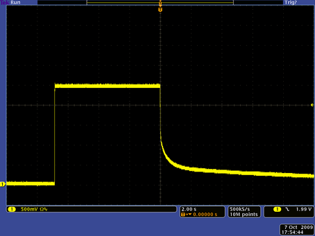
Rising edge is power on, falling edge is power off. Note the horizontal time scale of 2 s/div. So to get below 0.3 V or so, it takes up to 30 seconds. If the power is switched back on when AVDD is above 0.3V, the DRS4 chip can get into a weird state, where probably many domino waves are started and the chip draws an enormous amount of current. Typically the linear regulator limits the current, so the 2.5V drops to ~1.5V, and the board is not working. If people are aware of this and always wait >30sec. before turning the power on again, this is fine, but people might forget.
So the solution is to put a resistor (typically 100 Ohm to 1 kOhm) parallel to the 4.7 uF capacitor in order to have some resistive current load of a few mA. The discharge then looks like this:
Note the horizontal scale of 10ms/div. So after 30 ms AVDD is discharged and powering on the chip again does not do any harm. The same should be done to DVDD. |
|
12
|
Tue Oct 6 11:20:39 2009 |
Stefan Ritt | VDD instability | It has turned out that the stability of the AVDD and DVDD power supplies for the DRS4 are very critical. On the evaluation board I use a REG1117-2.5, on our VME board I use a ADP3338-2.5 for the DVDD power supply. When the domino wave is started, the power consumption of the DRS4 chip jumps up by ~40 mA, which has to be compensated by the linear regulator. Following screen shot shows what happens:
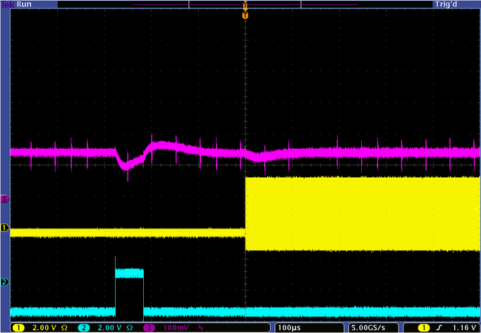
The blue trace is the DWRITE signal indicating the sampling phase when high. The yellow is the SRCLK showing when the readout takes place. The pink is now the DVDD power. It can be clearly seen that there is a dip of ~50 mV when the domino wave starts, a positive dip when it stops and another smaller dip when the readout starts. This causes strange effects: If the trigger arrives during the first dip, the actual sampling takes place when the DVDD is ~50 mV smaller, which leads to a baseline shift of a sampled 0V DC input voltage of about the same amount (-50 mV).
The obvious improvement is to put a huge capacitor on the power supply, but that does not help much:
The dip gets a bit smaller, but it's still there. So a better solution would be to use a faster LDO regulator. Please take care of this if you plan a new design.
Furthermore, I believe that the chip internally has some "warmup" phase, where the die heats up a bit when the additional 40 mA are drawn. So a "good" solution is to wait some time after starting the domino wave until one allows for triggers. Tests showed that a few milliseconds are necessary to keep the baseline shifts below a few millivolts. This of course decreases the dead time of the system significantly, so one has to choose the proper balance between increase dead time and increased base line shift. On some applications where a baseline shift is not an issue, one could opt for the minimum dead time. |
|
11
|
Thu Jul 9 09:11:03 2009 |
Stefan Ritt | Current problems with drs_exam.cpp | The current version of the DRS readout example program drs_exam.cpp has two problems:
- The sampling frequency cannot be changed, it will always stay in the region around 5 GSPS
- The waveform obtained by GetWave is rotated such that the first DRS cell corresponds to the first array bin
Both problems have been fixed and the fix will be contained in an upcoming software release. |
|
10
|
Tue Jul 7 16:39:57 2009 |
Stefan Ritt | Power up problem and remedy | Maybe some of you have experienced that the DRS4 chip can get pretty hot after power up. After it's initialized the first time, the power consumption goes back to normal. I finally found the cause of this problem and have a remedy. Here is the new paragraph from the updated data sheet:
During power-up, care has to be taken that the DENABLE and DWRITE signals are low. If not, the domino wave can get started before the power supply voltages are stable, which brings the DRS4 chip into a state where it draws a considerable amount of current and heats up significantly. This can be problematic if the signals are directly generated by a FPGA, since most FPGAs have internal pull-up resistors which get activated during the configuration phase of the FPGA. In such a case, the DENABLE and DWRITE signals should be connected to GND with a pull down resistor. This resistor should be much smaller than the FPGA pull-up resistor in order to keep the signals close to GND during the FPGA configuration. A typical value is 4.7 kOhm.
The attached schematics shows the location of the two required resistors. |
| Attachment 1: typical_mode.gif
|

|
|
9
|
Wed Jun 10 12:46:43 2009 |
Stefan Ritt | Input range switch added in Version 2.1.3 | A new software verison for the DRS4 Evaluation Board has been has been released. Version 2.1.3 adds a switch for the input range of the DRS4 board. Once can choose between -0.5V...0.5V and 0V...1V:
A board firmware update is not necessary for this. It was originally planned to have even a negative range -1V...0V, but this is not possible with the current board design. People who want to record negative pulses have to use an inverter to produce positive pulses. In a future version of the board it might be possible to include this functionality since this is determined by the analog front-end and not the DRS4 chip. |
|
8
|
Wed Apr 29 07:57:33 2009 |
Stefan Ritt | Simple example application to read a DRS evaluation board |
| Stefan Ritt wrote: |
|
Several people asked for s simple application to guide them in writing their own application to read out a DRS board. Such an application has been added in software revions 2.1.1 and is attached to this message. This example program drs_exam.cpp written in C++ does the following necessary steps to access a DRS board:
- Crate a "DRS" object and scan all USB devices
- Display found DRS boards
- Initialize the first found board and set the sampling frequency to 5 GSPS
- Enable internal trigger on channel #1 with 250 mV threshold
- Start acquisition and wait for a trigger
- Read two waveforms (both time and amplitude)
- Repeat this 10 times
I know that we are still missing a good documentation for the DRS API, but I have not yet found the time to do that. I hope the example program is enough for most people to start writing own programs. For Windows users (MS Visual C++ 8.0) there is a drs.sln project file, and for linux users there is a Makefile which can be used to compile this example program.
|
One note: The program drs_exam.cpp published in the previous message needs the current version of the DRS library in DRS.cpp and DRS.h. They are contained in the software release 2.1.1 which has to be downloaded. For simplicity, I attached the two files to this message. |
| Attachment 1: DRS.cpp
|
/********************************************************************

  Name:         DRS.cpp
  Created by:   Stefan Ritt, Matthias Schneebeli

  Contents:     Library functions for DRS mezzanine and USB boards

  $Id: DRS.cpp 13351 2009-04-28 11:12:54Z ritt@PSI.CH $

\********************************************************************/

#include <stdio.h>
#include <math.h>
#include <string.h>
#include <stdlib.h>
#include <time.h>
#include <assert.h>
#include <algorithm>
#include <sys/stat.h>
#include "strlcpy.h"

#ifdef _MSC_VER
#pragma warning(disable:4996)
#   include <windows.h>
#   include <direct.h>
#else
#   include <unistd.h>
#   include <sys/time.h>
inline void Sleep(useconds_t x)
{
   usleep(x * 1000);
}
#endif

#ifdef _MSC_VER
#include <conio.h>
#define drs_kbhit() kbhit()
#else
#include <sys/ioctl.h>
int drs_kbhit()
{
   int n;

   ioctl(0, FIONREAD, &n);
   return (n > 0);
}
static inline int getch()
{
   return getchar();
}
#endif

#include <DRS.h>

#ifdef _MSC_VER
extern "C" {
#endif

#include <mxml.h>

#ifdef _MSC_VER
}
#endif

/*---- minimal FPGA firmvare version required for this library -----*/
const int REQUIRED_FIRMWARE_VERSION_DRS2 = 5268;
const int REQUIRED_FIRMWARE_VERSION_DRS3 = 6981;
const int REQUIRED_FIRMWARE_VERSION_DRS4 = 13191;

/*---- VME addresses -----------------------------------------------*/
#ifdef HAVE_VME
/* assuming following DIP Switch settings:

   SW1-1: 1 (off)       use geographical addressing (1=left, 21=right)
   SW1-2: 1 (off)       \
   SW1-3: 1 (off)        >  VME_WINSIZE = 8MB, subwindow = 1MB
   SW1-4: 0 (on)        /
   SW1-5: 0 (on)        reserverd
   SW1-6: 0 (on)        reserverd
   SW1-7: 0 (on)        reserverd
   SW1-8: 0 (on)       \
                        |
   SW2-1: 0 (on)        |
   SW2-2: 0 (on)        |
   SW2-3: 0 (on)        |
   SW2-4: 0 (on)        > VME_ADDR_OFFSET = 0
   SW2-5: 0 (on)        |
   SW2-6: 0 (on)        |
   SW2-7: 0 (on)        |
   SW2-8: 0 (on)       /

   which gives
     VME base address = SlotNo * VME_WINSIZE + VME_ADDR_OFFSET
                      = SlotNo * 0x80'0000
*/
#define GEVPC_BASE_ADDR           0x00000000
#define GEVPC_WINSIZE               0x800000
#define GEVPC_USER_FPGA   (GEVPC_WINSIZE*2/8)
#define PMC1_OFFSET                  0x00000
#define PMC2_OFFSET                  0x80000
#define PMC_CTRL_OFFSET              0x00000    /* all registers 32 bit */
#define PMC_STATUS_OFFSET            0x10000
#define PMC_FIFO_OFFSET              0x20000
#define PMC_RAM_OFFSET               0x40000
#endif                          // HAVE_VME
/*---- USB addresses -----------------------------------------------*/
#define USB_TIMEOUT                     1000    // one second
#ifdef HAVE_USB
#define USB_CTRL_OFFSET                 0x00    /* all registers 32 bit */
#define USB_STATUS_OFFSET               0x40
#define USB_RAM_OFFSET                  0x80
#define USB_CMD_IDENT                      0    // Query identification
#define USB_CMD_ADDR                       1    // Address cycle
#define USB_CMD_READ                       2    // "VME" read <addr><size>
#define USB_CMD_WRITE                      3    // "VME" write <addr><size>
#define USB_CMD_READ12                     4    // 12-bit read <LSB><MSB>
#define USB_CMD_WRITE12                    5    // 12-bit write <LSB><MSB>

#define USB2_CMD_READ                      1
#define USB2_CMD_WRITE                     2
#define USB2_CTRL_OFFSET             0x00000    /* all registers 32 bit */
#define USB2_STATUS_OFFSET           0x10000
#define USB2_FIFO_OFFSET             0x20000
#define USB2_RAM_OFFSET              0x40000
#endif                          // HAVE_USB

/*---- Register addresses ------------------------------------------*/

#ifndef T_CTRL
#define T_CTRL                             1
#define T_STATUS                           2
#define T_RAM                              3
#define T_FIFO                             4
#endif

#define REG_CTRL                     0x00000    /* 32 bit control reg */
#define REG_DAC_OFS                  0x00004
#define REG_DAC0                     0x00004
#define REG_DAC1                     0x00006
#define REG_DAC2                     0x00008
#define REG_DAC3                     0x0000A
#define REG_DAC4                     0x0000C
#define REG_DAC5                     0x0000E
#define REG_DAC6                     0x00010
#define REG_DAC7                     0x00012
#define REG_CHANNEL_CONFIG           0x00014    // low byte
#define REG_CONFIG                   0x00014    // high byte
#define REG_CHANNEL_SPAN             0x00016
#define REG_FREQ_SET_HI              0x00018    // DRS2
#define REG_FREQ_SET_LO              0x0001A    // DRS2
#define REG_TRG_DELAY                0x00018    // DRS4
#define REG_FREQ_SET                 0x0001A    // DRS4
#define REG_TRIG_DELAY               0x0001C
#define REG_LMK_MSB                  0x0001C    // DRS4 Mezz
#define REG_CALIB_TIMING             0x0001E    // DRS2
#define REG_EEPROM_PAGE              0x0001E    // DRS4
#define REG_LMK_LSB                  0x0001E    // DRS4 Mezz

#define REG_MAGIC                    0x00000
#define REG_BOARD_TYPE               0x00002
#define REG_STATUS                   0x00004
#define REG_RDAC_OFS                 0x0000E
#define REG_RDAC0                    0x00008
#define REG_STOP_CELL0               0x00008
#define REG_RDAC1                    0x0000A
#define REG_STOP_CELL1               0x0000A
#define REG_RDAC2                    0x0000C
#define REG_STOP_CELL2               0x0000C
#define REG_RDAC3                    0x0000E
#define REG_STOP_CELL3               0x0000E
#define REG_RDAC4                    0x00000
#define REG_RDAC5                    0x00002
#define REG_RDAC6                    0x00014
#define REG_RDAC7                    0x00016
#define REG_EVENTS_IN_FIFO           0x00018
#define REG_EVENT_COUNT              0x0001A
#define REG_FREQ1                    0x0001C
#define REG_FREQ2                    0x0001E
#define REG_TEMPERATURE              0x00020
#define REG_TRIGGER_BUS              0x00022
#define REG_SERIAL_BOARD             0x00024
#define REG_VERSION_FW               0x00026

/*------------------------------------------------------------------*/

using namespace std;

#ifdef HAVE_USB
#define USB2_BUFFER_SIZE (1024*1024+10)
unsigned char static *usb2_buffer = NULL;
#endif

/*------------------------------------------------------------------*/

DRS::DRS()
:  fNumberOfBoards(0)
#ifdef HAVE_VME
    , fVmeInterface(0)
#endif
{
#ifdef HAVE_USB
   MUSB_INTERFACE *usb_interface;
#endif

#if defined(HAVE_VME) || defined(HAVE_USB)
   int index = 0, i = 0;
#endif

   memset(fError, 0, sizeof(fError));

#ifdef HAVE_VME
   unsigned short type, fw, magic, serial, temperature;
   mvme_addr_t addr;

   if (mvme_open(&fVmeInterface, 0) == MVME_SUCCESS) {

      mvme_set_am(fVmeInterface, MVME_AM_A32);
      mvme_set_dmode(fVmeInterface, MVME_DMODE_D16);

      /* check all VME slave slots */
      for (index = 2; index <= 21; index++) {

         /* check PMC1 */
         addr = GEVPC_BASE_ADDR + index * GEVPC_WINSIZE;        // VME board base address
         addr += GEVPC_USER_FPGA;       // UsrFPGA base address
         addr += PMC1_OFFSET;   // PMC1 offset

         mvme_set_dmode(fVmeInterface, MVME_DMODE_D16);
         i = mvme_read(fVmeInterface, &magic, addr + PMC_STATUS_OFFSET + REG_MAGIC, 2);
         if (i == 2) {
            if (magic != 0xC0DE) {
               printf("Found old firmware, please upgrade immediately!\n");
               fBoard[fNumberOfBoards] = new DRSBoard(fVmeInterface, addr, (index - 2) << 1);
               fNumberOfBoards++;
            } else {

               /* read board type */
               mvme_read(fVmeInterface, &type, addr + PMC_STATUS_OFFSET + REG_BOARD_TYPE, 2);
               type &= 0xFF;
               if (type == 2 || type == 3 || type == 4) {    // DRS2 or DRS3 or DRS4

                  /* read firmware number */
                  mvme_read(fVmeInterface, &fw, addr + PMC_STATUS_OFFSET + REG_VERSION_FW, 2);

                  /* read serial number */
                  mvme_read(fVmeInterface, &serial, addr + PMC_STATUS_OFFSET + REG_SERIAL_BOARD, 2);

                  /* read temperature register to see if CMC card is present */
                  mvme_read(fVmeInterface, &temperature, addr + PMC_STATUS_OFFSET + REG_TEMPERATURE, 2);

                  /* LED blinking */
#if 0
                  do {
                     data = 0x00040000;
                     mvme_write(fVmeInterface, addr + PMC_CTRL_OFFSET + REG_CTRL, &data, sizeof(data));
                     mvme_write(fVmeInterface, addr + PMC2_OFFSET + PMC_CTRL_OFFSET + REG_CTRL, &data,
                                sizeof(data));

                     Sleep(500);

                     data = 0x00000000;
                     mvme_write(fVmeInterface, addr + PMC_CTRL_OFFSET + REG_CTRL, &data, sizeof(data));
                     mvme_write(fVmeInterface, addr + PMC2_OFFSET + PMC_CTRL_OFFSET + REG_CTRL, data,
                                sizeof(data));

                     Sleep(500);

                  } while (1);
#endif

                  if (temperature == 0xFFFF) {
                     //printf("slot %d, fw %d, no CMC board in upper slot\n", index, fw);
                  } else {
                     //printf("slot %d, fw %d, CMC serial %d in upper slot\n", index, fw, serial);

                     fBoard[fNumberOfBoards] = new DRSBoard(fVmeInterface, addr, (index - 2) << 1);
                     if (fBoard[fNumberOfBoards]->HasCorrectFirmware())
                        fNumberOfBoards++;
                     else
                        sprintf(fError, "Wrong firmware version: board has %d, required is %d\n",
                                fBoard[fNumberOfBoards]->GetFirmwareVersion(),
                                fBoard[fNumberOfBoards]->GetRequiredFirmwareVersion());
                  }
               }
            }
         }

         /* check PMC2 */
         addr = GEVPC_BASE_ADDR + index * GEVPC_WINSIZE;        // VME board base address
         addr += GEVPC_USER_FPGA;       // UsrFPGA base address
         addr += PMC2_OFFSET;   // PMC2 offset

         mvme_set_dmode(fVmeInterface, MVME_DMODE_D16);
         i = mvme_read(fVmeInterface, &fw, addr + PMC_STATUS_OFFSET + REG_MAGIC, 2);
         if (i == 2) {
            if (magic != 0xC0DE) {
               printf("Found old firmware, please upgrade immediately!\n");
               fBoard[fNumberOfBoards] = new DRSBoard(fVmeInterface, addr, (index - 2) << 1 | 1);
               fNumberOfBoards++;
            } else {
... 5173 more lines ...
|
| Attachment 2: DRS.h
|
/********************************************************************
  DRS.h, S.Ritt, M. Schneebeli - PSI

  $Id: DRS.h 13347 2009-04-28 08:24:05Z ritt@PSI.CH $

********************************************************************/
#ifndef DRS_H
#define DRS_H
#include <stdio.h>
#include <string.h>

#ifdef HAVE_LIBUSB
#   ifndef HAVE_USB
#      define HAVE_USB
#   endif
#endif

#ifdef HAVE_USB
#   include <musbstd.h>
#endif                          // HAVE_USB

#ifdef HAVE_VME
#   include <mvmestd.h>
#endif                          // HAVE_VME

/* disable "deprecated" warning */
#ifdef _MSC_VER
#pragma warning(disable: 4996)
#endif

#ifndef NULL
#define NULL 0
#endif

/* transport mode */
#define TR_VME   1
#define TR_USB   2
#define TR_USB2  3

/* address types */
#define T_CTRL   1
#define T_STATUS 2
#define T_RAM    3
#define T_FIFO   4

/* control register bit definitions */
#define BIT_START_TRIG        (1<<0)    // write a "1" to start domino wave
#define BIT_REINIT_TRIG       (1<<1)    // write a "1" to stop & reset DRS
#define BIT_SOFT_TRIG         (1<<2)    // write a "1" to stop and read data to RAM
#define BIT_EEPROM_WRITE_TRIG (1<<3)    // write a "1" to write into serial EEPROM
#define BIT_EEPROM_READ_TRIG  (1<<4)    // write a "1" to read from serial EEPROM
#define BIT_AUTOSTART        (1<<16)
#define BIT_DMODE            (1<<17)    // (*DRS2*) 0: single shot, 1: circular
#define BIT_LED              (1<<18)    // 1=on, 0=blink during readout
#define BIT_TCAL_EN          (1<<19)    // switch on (1) / off (0) for 33 MHz calib signal
#define BIT_TCAL_SOURCE      (1<<20)
#define BIT_REFCLK_SOURCE    (1<<20)
#define BIT_FREQ_AUTO_ADJ    (1<<21)    // DRS2/3
#define BIT_TRANSP_MODE      (1<<21)    // DRS4
#define BIT_ENABLE_TRIGGER1  (1<<22)    // External LEMO/FP/TRBUS trigger
#define BIT_LONG_START_PULSE (1<<23)    // (*DRS2*) 0:short start pulse (>0.8GHz), 1:long start pulse (<0.8GHz)
#define BIT_READOUT_MODE     (1<<23)    // (*DRS3*) 0:start from first bin, 1:start from domino stop
#define BIT_DELAYED_START    (1<<24)    // DRS2: start domino wave 400ns after soft trigger, used for waveform
                                        // generator startup
#define BIT_NEG_TRIGGER      (1<<24)    // DRS4: use high-to-low trigger if set
#define BIT_ACAL_EN          (1<<25)    // connect DRS to inputs (0) or to DAC6 (1)
#define BIT_TRIGGER_DELAYED  (1<<26)    // select delayed trigger from trigger bus
#define BIT_DACTIVE          (1<<27)    // keep domino wave running during readout
#define BIT_STANDBY_MODE     (1<<28)    // put chip in standby mode
#define BIT_TR_SOURCE1       (1<<29)    // trigger source selection bits
#define BIT_TR_SOURCE2       (1<<30)    // trigger source selection bits
#define BIT_ENABLE_TRIGGER2  (1<<31)    // analog threshold (internal) trigger

/* status register bit definitions */
#define BIT_RUNNING           (1<<0)    // one if domino wave running or readout in progress
#define BIT_NEW_FREQ1         (1<<1)    // one if new frequency measurement available
#define BIT_NEW_FREQ2         (1<<2)
#define BIT_PLL_LOCKED0       (1<<1)    // 1 if PLL has locked (DRS4 evaluation board only)
#define BIT_PLL_LOCKED1       (1<<2)    // 1 if PLL DRS4 B has locked (DRS4 mezzanine board only)
#define BIT_PLL_LOCKED2       (1<<3)    // 1 if PLL DRS4 C has locked (DRS4 mezzanine board only)
#define BIT_PLL_LOCKED3       (1<<4)    // 1 if PLL DRS4 D has locked (DRS4 mezzanine board only)
#define BIT_EEPROM_BUSY       (1<<5)    // 1 if EEPROM operation in progress

/* configuration register bit definitions */
#define BIT_CONFIG_DMODE      (1<<8)    // 0: single shot, 1: circular
#define BIT_CONFIG_PLLEN      (1<<9)    // write a "1" to enable the internal PLL
#define BIT_CONFIG_WSRLOOP   (1<<10)    // write a "1" to connect WSROUT to WSRIN internally

enum DRSBoardConstants {
   kNumberOfChannelsV2          =   10,
   kNumberOfChannelsV4          =    9,
   kNumberOfCalibChannelsV3     =   10,
   kNumberOfCalibChannelsV4     =    9,
   kNumberOfBins                = 1024,
   kNumberOfChips               =    2,
   kFrequencyCacheSize          =   10,
   kBSplineOrder                =    4,
   kPreCaliculatedBSplines      = 1000,
   kPreCaliculatedBSplineGroups =    5,
   kNumberOfADCBins             = 4096,
   kBSplineXMinOffset           =   20,
   kMaxNumberOfClockCycles      =  100,
};

enum DRSErrorCodes {
   kSuccess                     =  0,
   kInvalidTriggerSignal        = -1,
   kWrongChannelOrChip          = -2,
   kInvalidTransport            = -3,
   kZeroSuppression             = -4,
   kWaveNotAvailable            = -5
};

/*---- callback class ----*/

class DRSCallback
{
public:
   virtual void Progress(int value) = 0;
   virtual ~DRSCallback() {};
};

/*------------------------*/

class DRSBoard;

class ResponseCalibration {
protected:

   class CalibrationData {
   public:
      class CalibrationDataChannel {
      public:
         unsigned char   fLimitGroup[kNumberOfBins];           //!
         float           fMin[kNumberOfBins];                  //!
         float           fRange[kNumberOfBins];                //!
         short           fOffset[kNumberOfBins];               //!
         short           fGain[kNumberOfBins];                 //!
         unsigned short  fOffsetADC[kNumberOfBins];            //!
         short          *fData[kNumberOfBins];                 //!
         unsigned char  *fLookUp[kNumberOfBins];               //!
         unsigned short  fLookUpOffset[kNumberOfBins];         //!
         unsigned char   fNumberOfLookUpPoints[kNumberOfBins]; //!
         float          *fTempData;                            //!

      private:
         CalibrationDataChannel(const CalibrationDataChannel &c);              // not implemented
         CalibrationDataChannel &operator=(const CalibrationDataChannel &rhs); // not implemented

      public:
         CalibrationDataChannel(int numberOfGridPoints)
         :fTempData(new float[numberOfGridPoints]) {
            int i;
            for (i = 0; i < kNumberOfBins; i++) {
               fData[i] = new short[numberOfGridPoints];
            }
            memset(fLimitGroup,           0, sizeof(fLimitGroup));
            memset(fMin,                  0, sizeof(fMin));
            memset(fRange,                0, sizeof(fRange));
            memset(fOffset,               0, sizeof(fOffset));
            memset(fGain,                 0, sizeof(fGain));
            memset(fOffsetADC,            0, sizeof(fOffsetADC));
            memset(fLookUp,               0, sizeof(fLookUp));
            memset(fLookUpOffset,         0, sizeof(fLookUpOffset));
            memset(fNumberOfLookUpPoints, 0, sizeof(fNumberOfLookUpPoints));
         }
         ~CalibrationDataChannel() {
            int i;
            delete fTempData;
            for (i = 0; i < kNumberOfBins; i++) {
               delete fData[i];
               delete fLookUp[i];
            }
         }
      };

      bool                    fRead;                                  //!
      CalibrationDataChannel *fChannel[10];                           //!
      unsigned char           fNumberOfGridPoints;                    //!
      int                     fHasOffsetCalibration;                  //!
      float                   fStartTemperature;                      //!
      float                   fEndTemperature;                        //!
      int                    *fBSplineOffsetLookUp[kNumberOfADCBins]; //!
      float                 **fBSplineLookUp[kNumberOfADCBins];       //!
      float                   fMin;                                   //!
      float                   fMax;                                   //!
      unsigned char           fNumberOfLimitGroups;                   //!
      static float            fIntRevers[2 * kBSplineOrder - 2];

   private:
      CalibrationData(const CalibrationData &c);              // not implemented
      CalibrationData &operator=(const CalibrationData &rhs); // not implemented

   public:
      CalibrationData(int numberOfGridPoints);
      ~CalibrationData();
      static int CalculateBSpline(int nGrid, float value, float *bsplines);
      void       PreCalculateBSpline();
      void       DeletePreCalculatedBSpline();
   };

   // General Fields
   DRSBoard        *fBoard;

   double           fPrecision;

   // Fields for creating the Calibration
   bool             fInitialized;
   bool             fRecorded;
   bool             fFitted;
   bool             fOffset;
   bool             fCalibrationValid[2];

   int              fNumberOfPointsLowVolt;
   int              fNumberOfPoints;
   int              fNumberOfMode2Bins;
   int              fNumberOfSamples;
   int              fNumberOfGridPoints;
   int              fNumberOfXConstPoints;
   int              fNumberOfXConstGridPoints;
   double           fTriggerFrequency;
   int              fShowStatistics;
   FILE            *fCalibFile;

   int              fCurrentLowVoltPoint;
   int              fCurrentPoint;
   int              fCurrentSample;
   int              fCurrentFitChannel;
   int              fCurrentFitBin;

   float           *fResponseX[10][kNumberOfBins];
   float           *fResponseY;
   unsigned short **fWaveFormMode3[10];
   unsigned short **fWaveFormMode2[10];
   unsigned short **fWaveFormOffset[10];
   unsigned short **fWaveFormOffsetADC[10];
   unsigned short  *fSamples;
   int             *fSampleUsed;

   float           *fPntX[2];
   float           *fPntY[2];
   float           *fUValues[2];
   float           *fRes[kNumberOfBins];
   float           *fResX[kNumberOfBins];

   double          *fXXFit;
   double          *fYYFit;
   double          *fWWFit;
   double          *fYYFitRes;
   double          *fYYSave;
   double          *fXXSave;
   double          fGainMin;
   double          fGainMax;

   float          **fStatisticsApprox;
   float          **fStatisticsApproxExt;

   // Fields for applying the Calibration
   CalibrationData *fCalibrationData[kNumberOfChips];

private:
         ResponseCalibration(const ResponseCalibration &c);              // not implemented
         ResponseCalibration &operator=(const ResponseCalibration &rhs); // not implemented

public:
   ResponseCalibration(DRSBoard* board);
   ~ResponseCalibration();

   void   SetCalibrationParameters(int numberOfPointsLowVolt, int numberOfPoints, int numberOfMode2Bins,
                                   int numberOfSamples, int numberOfGridPoints, int numberOfXConstPoints,
                                   int numberOfXConstGridPoints, double triggerFrequency, int showStatistics = 0);
   void   ResetCalibration();
   bool   RecordCalibrationPoints(int chipNumber);
   bool   RecordCalibrationPointsV3(int chipNumber);
   bool   RecordCalibrationPointsV4(int chipNumber);
   bool   FitCalibrationPoints(int chipNumber);
   bool   FitCalibrationPointsV3(int chipNumber);
   bool   FitCalibrationPointsV4(int chipNumber);
   bool   OffsetCalibration(int chipNumber);
   bool   OffsetCalibrationV3(int chipNumber);
   bool   OffsetCalibrationV4(int chipNumber);
   double GetTemperature(unsigned int chipIndex);

   bool   WriteCalibration(unsigned int chipIndex);
   bool   WriteCalibrationV3(unsigned int chipIndex);
   bool   WriteCalibrationV4(unsigned int chipIndex);
   bool   ReadCalibration(unsigned int chipIndex);
   bool   ReadCalibrationV3(unsigned int chipIndex);
   bool   ReadCalibrationV4(unsigned int chipIndex);
   bool   Calibrate(unsigned int chipIndex, unsigned int channel, float *adcWaveform,
                    float *uWaveform, float threshold, bool offsetCalib);
   bool   Calibrate(unsigned int chipIndex, unsigned int channel, unsigned short *adcWaveform, unsigned short *uWaveform,
                    int triggerCell, float threshold, bool offsetCalib);
   bool   SubtractADCOffset(unsigned int chipIndex, unsigned int channel, unsigned short *adcWaveform,
                            unsigned short *adcCalibratedWaveform, unsigned short newBaseLevel);
   bool   IsRead(int chipIndex) const { return fCalibrationValid[chipIndex]; }
   double GetPrecision() const { return fPrecision; };

   double GetOffsetAt(int chip,int chn,int bin) const { return fCalibrationData[chip]->fChannel[chn]->fOffset[bin]; };
   double GetGainAt(int chip,int chn,int bin) const { return fCalibrationData[chip]->fChannel[chn]->fGain[bin]; };
... 336 more lines ...
|
|
7
|
Tue Apr 28 11:44:07 2009 |
Stefan Ritt | Simple example application to read a DRS evaluation board | Several people asked for s simple application to guide them in writing their own application to read out a DRS board. Such an application has been added in software revions 2.1.1 and is attached to this message. This example program drs_exam.cpp written in C++ does the following necessary steps to access a DRS board:
- Crate a "DRS" object and scan all USB devices
- Display found DRS boards
- Initialize the first found board and set the sampling frequency to 5 GSPS
- Enable internal trigger on channel #1 with 250 mV threshold
- Start acquisition and wait for a trigger
- Read two waveforms (both time and amplitude)
- Repeat this 10 times
I know that we are still missing a good documentation for the DRS API, but I have not yet found the time to do that. I hope the example program is enough for most people to start writing own programs. For Windows users (MS Visual C++ 8.0) there is a drs.sln project file, and for linux users there is a Makefile which can be used to compile this example program.
|
| Attachment 1: drs_exam.cpp
|
/********************************************************************\

  Name:         drs_exam.cpp
  Created by:   Stefan Ritt

  Contents:     Simple example application to read out a DRS4
                evaluation board

  $Id: drs_exam.cpp 13344 2009-04-28 07:34:45Z ritt@PSI.CH $

\********************************************************************/

#include <math.h>

#ifdef _MSC_VER

#include <windows.h>

#elif defined(OS_LINUX)

#define O_BINARY 0

#include <unistd.h>
#include <ctype.h>
#include <sys/ioctl.h>
#include <errno.h>

#define DIR_SEPARATOR '/'

#endif

#include <stdio.h>
#include <string.h>
#include <stdlib.h>

#include "strlcpy.h"
#include "DRS.h"

/*------------------------------------------------------------------*/

int main()
{
   int i, j, nBoards;
   DRS *drs;
   DRSBoard *b;
   float time_array[1024];
   float wave_array[8][1024];

   /* do initial scan */
   drs = new DRS();

   /* show any found board(s) */
   for (i=0 ; i<drs->GetNumberOfBoards() ; i++) {
      b = drs->GetBoard(i);
      printf("Found DRS4 evaluation board, serial #%d, firmware revision %d\n",
         b->GetBoardSerialNumber(), b->GetFirmwareVersion());
   }

   /* exit if no board found */
   nBoards = drs->GetNumberOfBoards();
   if (nBoards == 0) {
      printf("No DRS4 evaluation board found\n");
      return 0;
   }

   /* continue working with first board only */
   b = drs->GetBoard(0);

   /* initialize board */
   b->Init();

   /* set sampling frequency */
   b->SetFrequency(5);

   /* enable transparent mode needed for analog trigger */
   b->SetTranspMode(1);

   /* use following line to disable hardware trigger */
   //b->EnableTrigger(0, 0);

   /* use following line to enable external hardware trigger (Lemo) */
   //b->EnableTrigger(1, 0);

   /* use following lines to enable hardware trigger on CH1 at 250 mV positive edge */
   b->EnableTrigger(0, 1);              // lemo off, analog trigger on
   b->SetTriggerSource(0);              // use CH1 as source
   b->SetTriggerLevel(0.25, false, 0);  // 0.25 V, positive edge, zero delay

   /* repeat ten times */
   for (j=0 ; j<10 ; j++) {

      /* start board (activate domino wave) */
      b->StartDomino();

      /* wait for trigger */
      printf("Waiting for trigger...");
      while (b->IsBusy());

      /* read all waveforms */
      b->TransferWaves(0, 8);

      /* read time (X) array in ns */
      b->GetTime(0, time_array);

      /* decode waveform (Y) array first channel in mV */
      b->GetWave(0, 0, wave_array[0]);

      /* decode waveform (Y) array second channel in mV*/
      b->GetWave(0, 1, wave_array[1]);

      /* process waveform: add here some code to display or save waveform X=time[i], Y=wave_array[n][i] */

      /* print some progress indication */
      printf("\rEvent #%d read successfully\n", j);
   }

   /* delete DRS object -> close USB connection */
   delete drs;
}
|
|
6
|
Mon Apr 27 15:09:49 2009 |
Stefan Ritt | Amplitude and Timing calibration for DRS4 Evaluation Board | This is a quick notification to all users of the current DRS4 evaluation board.
As you all know, the DRS4 chip needs some calibration for each individual cell which corrects the offset and the non-equidistant width in time. While the first evaluation boards have been shipped without this calibration, the current version of the software implements a full amplitude and timing calibration. The offset correction reduces the noise of the board by almost an order of magnitude to below 1 mV RMS. The timing calibration using an on-board reference clock allows a timing accuracy in the order of 10 ps. To illustrate that the following two pictures show a reference clock signal before and after timing calibration:
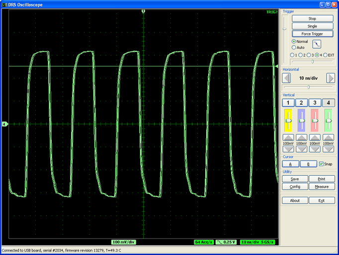
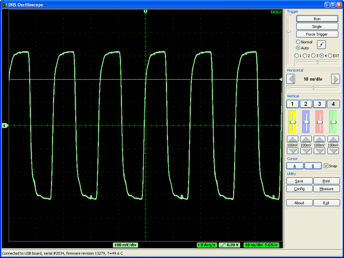
The integral temporal nonlineairy at 5 GSPS before timing calibration is about 600 ps as can be seen by the jitter of the overlaid waveforms.
In order to do a timing calibration, the firmware revison 13297 or later is required. The current software package 2.1 contains an updated firmware, but unfortunately one needs a Xilinx download cable to flash this new firmware (see http://drs.web.psi.ch/download/ under "Software Versions"). If some people want an update but do not want to buy such a cable, we offer a free update at our institute (just the postage has to be paid). The old evaluation board (Rev. 1.0, plastic housing) can unfortunately not be updated.
After the offset calibration is made, there are small (~20mV) short spikes left. They probably come from some cross-talk between the USB interface and the analog part of the board. This is currently under investigation. If new updates become available, they will be announced in this forum.
April 27th, 2009,
Stefan Ritt |
|
5
|
Mon Feb 23 09:24:24 2009 |
Stefan Ritt | Rise-time measurements | Many applications using the DRS4 need to measure fast rising signals, like for PMTs or MCPs. This short note shows the minimal rise-times which can be measured with different input signal conditioning.
Evaluation Board
The evaluation board contains four passive transformers ADT1-1WT from Mini-Circuits to convert the single-ended input signal into a differential signal. Although these parts are rated 800 MHz bandwidth (-3dB), they have hard time to drive the DRS4 inputs. This is because at high frequencies the input impedance of DRS4 becomes pretty small (~20 Ohm at 500 MHz) due to its capacitive nature. Furthermore, each transformer drives two DRS4 inputs (channel cascading) which enhances this problem by a factor of two. We made a quick test sending a signal to the evaluation board with a rise time of 277ps and a fall time of 280ps. The result measured with the evaluation board is seen here:
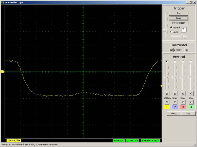
The measured rise-time (10%-90%) is only about 2ns. Disconnecting the second channel from each transformer improves this situation a bit:
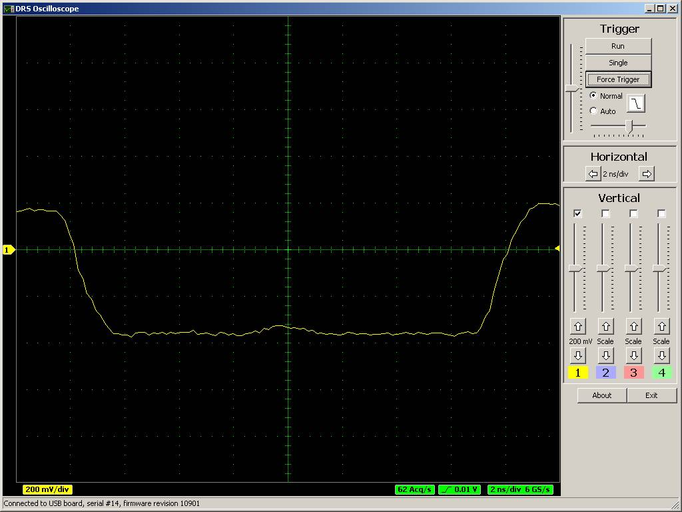
so the rise-time comes down to ~1.6ns.
Active ADA4937 driver
We tested the behavior using an active buffer ADA4937 to replace the passive transformer. Without the DRS4 connected to this buffer, we measured with the oscilloscope a rise time of 408ps and a fall time of 644ps. When we connect the DRS4 (single channel), this values increase to 702ps (rise) and 1400ps (fall), all measured with a differential oscilloscope probe (WL300 4 GHz Bandwidth, LeCroy 7300A, 3 GHz Bandwidth). In this case the rise time seen by the DRS4 is wieth ~700ps accordingly shorter:
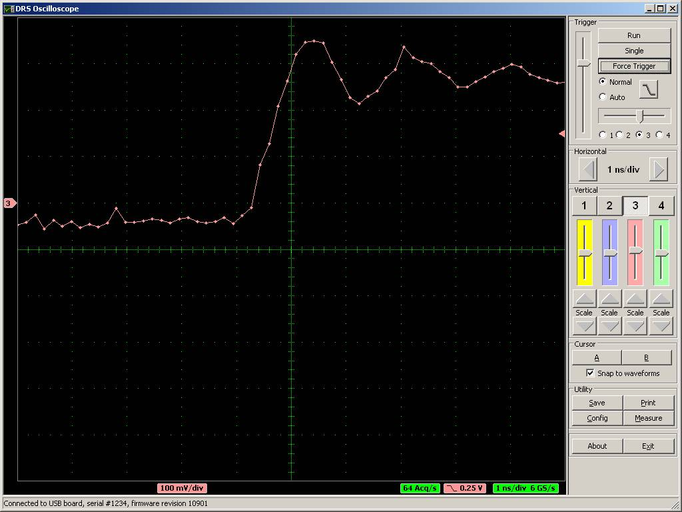
(The signal was not properly terminated and therefore we have a small overswing).
Conclusion
To obtain an optimal rise-time measurement, the design of the input stage is rather important. A fast active driver seems to do a better job than a passive transformer (which was used on the evaluation board for power reasons). Connecting only one DRS4 channel to the input improves the rise-time measurement significantly. If channel cascading is still needed, a design should use one driver for each channel, and not driver two or more DRS4 inputs from a single buffer.
If anybody comes up with an even better input driver, I'm happy to publish the results here. |
|
4
|
Wed Feb 11 12:21:07 2009 |
Stefan Ritt | Corrected datasheet Rev. 0.8 | Please note the new datasheet Rev. 0.8 available from the DRS web site. It fixes the label of pin #76, which was AGND but is actualy AVDD. The input IN8+ is located at pin #20 and not at pin #19 as described in the old table 2. |
|
3
|
Wed Jan 14 13:41:44 2009 |
Stefan Ritt | External Trigger Input requirements |
Another tricky issue comes from the fact that the external TTL trigger and the comparator are in a logical OR. So if the comparator level is set such that the signal is always over the threshold, the trigger is always "on" and the TTL trigger does not have any effect. It is therefore necessary to set the analog trigger level to a very high value in order to make the TTL trigger work. |
|
2
|
Wed Jan 14 12:02:04 2009 |
Stefan Ritt | External Trigger Input requirements | Several people mentioned that the external trigger input (TTL) does not work on the DRS4 Evaluation Board Rev. 1.1. This is not true. The requirement however is that the input signal must exceed approximately 1.8V. Since the input is terminated with 50 Ohms, not all TTL drivers may deliver enough current to exceed this threshold. To verify this, the trigger signal can be monitored with an oscilloscope at test point J24. Only if the input signal exceeds 1.8V, the signal will be seen at J24 and correctly trigger the FPGA. If the TTL driver is too weak, the termination resistor R9 can be optionally removed, but care should then be taken that reflections in the trigger input do not cause double triggers. The locations of the tap point for the input signal, the termination resistor R9 and the tap point J24 after the input level converter U5 are shown in this image:
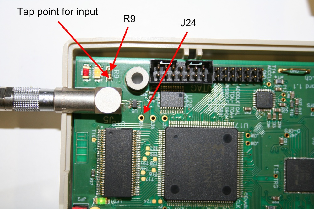
|
|
1
|
Mon Dec 15 13:37:38 2008 |
Stefan Ritt | Welcome | Welcome to the DRS4 Discussion Forum. This forum contains information and discussions related to the DRS4 chip. Please subscribe to this forum to receive automatic email updates. If you have any technical questions, please feel free to post it here. |
|